Citation:
Marino, MD (2018) Architectural Impacts of RFiop: RF to Address I/O Pad and Memory Controller
Scalability. IEEE Transactions on Very Large Scale Integration (VLSI) Systems. ISSN 1063-8210
DOI: https://doi.org/10.1109/TVLSI.2018.2821004
Link to Leeds Beckett Repository record:
http://eprints.leedsbeckett.ac.uk/4937/
Document Version:
Article
The aim of the Leeds Beckett Repository is to provide open access to our research, as required by
funder policies and permitted by publishers and copyright law.
The Leeds Beckett repository holds a wide range of publications, each of which has been
checked for copyright and the relevant embargo period has been applied by the Research Services
team.
We operate on a standard take-down policy.
If you are the author or publisher of an output
and you would like it removed from the repository, please
contact us
and we will investigate on a
case-by-case basis.
Architectural Impacts of
RF iop
:
RF
to Address
I
/
O P
ad and Memory Controller Scalability
Mario D. Marino
Member, IEEE,
Leeds Beckett University, [email protected]
Abstract— Despite power boundaries, Moore’s law is still present via scaling the number of cores, which keeps adding demands for more memory bandwidth requested by these cores. To obtain higher bandwidth levels it is fundamental to address memory controller (MC) scalability. However, MC scalability growth is limited by I/O pin counts scaling. To underline MC and pin scaling, a radio frequency( RF) I/ O pad-scalable package-based (RF iop) memory organization is further investigated.
In RF iop, a radio-frequency pad (RFpad) is defined as a quilt-packaging (QP) coplanar waveguide (CPW) employed at radio-frequency (RF) ranges. An RFpad connects a rank to an RFMC which is formed by coupling MCs to RF TX/RX. By using QP package to explore the architectural benefits of laying out ranks,RF iopreplaces the traditional memory path with an RF-based one, whilst exploring the scalability of RFpads/RFMCs via RF signaling. When evaluating RF iop, our findings show that bandwidth/performance are enhanced by around 4.3x which can be viewed as a diminution in transaction queue occupancy/latency as well as using a reduced and scalable 4-8 RFpads per RFMC. RF iop architectural area benefits allow bandwidth/performance improvements of around 3.2x, whilst reducing interconnection energy up to 78%.
Index Terms—memory, controller, bandwidth, I/O pin, RF
I. INTRODUCTION
Given Moore’s law lasting behaviour, higher transistor den-sities have allowed core count growth along different processor generations. Other than the dominant and restrictive power wall problem, as more cores are included, memory bandwidth contention is further increased, which is likely to decrease performance. On the applications side, internet of things[1] and big data science applications are likely to further increase the pressure on the memory system.
Current digital memory design has mostly focused on (i) frequency rather than (ii) width, whilst keeping area/density upper boundary limits for I/O pad/pin counts[2]. For example, (i) current DDR-solutions present typical memory data rates in the 1333-2400MT/s range in multicores, up to 5000MT/s in manycores, and 667-1333MT/s in embedded ones[2].
Given that larger frequencies dramatically impact power, memory parallelism via larger (ii) widths is a potential solution. Larger widths can be explored via (ii.1) a larger number of memory controllers (MCs) and/or via employing (ii.2) ranks (which are commercially known as dual in-line memory module or DIMM, that are sets of memory banks with data output aggregated and sharing addresses) with larger widths.
(ii.1) Having larger width means employing a larger number of MCs (MC counts or MC scalability). Despite low cost and proper design alternative for low numbers of MCs, given ITRS
pin-count limitations[3], as cores count tend to tens/hundreds, DDR technologies present significant I/O pin counts scalability restrictions, thus limiting the number of MCs, which further restricts bandwidth and performance. For example, 16-core Bulldozer[4] and 64-core Tile64[5] processors have 4 MCs.
More advanced commercial solutions such as Intel FBDIMM[6], Hyper Memory Cube (HMC)[7], and RAMBUS XDR2[8] all of which even employing serialization, accompa-nied by adaptive equalization in the latter one, are still bound by unscalable I/O pins, which restricts the scalability of the number of MCs and as a consequence bandwidth benefits. Alternatively, using (ii.2) much wider ranks and presenting no I/O pins/scalability restrictions, scaling MCs in 3Dstacking is reported[9] to be limited by temperature when scaling ranks, thus restricting memory parallelism.
Optical- and radio-frequency-(RF)-based memory are nologies that combine telecommunication transmission tech-niques and fast media on the memory path to address I/O pin scalability. Former solutions employ wavelength division multiplexing (WDM) and optical fibers to connect processor and memory through optical MCs and scalable optical-pins[10]. Still restricted in terms of development costs, optical trans-mission has advanced significantly in regards to temperature sensitiveness[11]. Instead, by sharing manufacturability with CMOS, RF shares its low costs, whilst remaining advantageous in terms of energy and millimeter-range delays when compared to optical transmission as reported in [12].
Very importantly, being appointed[13] as one of the areas that can improve processor performance the most, Tam et al.[14] state that in the 1-10cm range (which is well within regular package distances[13]) RF-transmission is more energy-efficient than optical and digital (traditional) ones.
Coplanar waveguide (CPW)1 and microstrip2 are examples of types of RF-interconnection that could be employed along the memory path and placed on-package. In particular, CPW quilt-packaging (QP)3 lines[15] were prototyped and manu-factured, which demonstrates the viability of an on-package
1CPW is an RF waveguide that has a central metallic strip line composed
of two different slits, which are separated by a ground plane; the strip is manufactured on the upper part of the dielectric.
2Generally employed in RF on-chip communications and composed by a
trace of metal on top of a substrate.
3quilt packaging (QP) is a technique where quilt lines [15] are introduced:
RF-interconnection that could be used to connect processor to memory.
In the RF domain of scalable-width solutions,RF iopsystem employs the package area which fits ranks (which are assumed to be manufactured as dies) and QP lines to connect ranks and MCs as a likely solution to improve bandwidth. Exploring Polka et al.’s[13] guidelines towards improving bandwidth on the package area, compared to RF iop organisation [16] previously proposed, this report further leverages the space of scalable-width memory solutions through the following contributions:
• Given potential growth on the number of cores, RF iop bandwidth and latency are further evaluated and a sensitive analysis is performed under a larger number of cores (twice as the previous publication).
• Through detailed-accurate system simulation,RF iop per-formance, area and power architectural implications are further investigated when replacing MC with an equivalent RFMC, whilst the most important ones are identified.
• An RF behavioral model of the RFpads (which are defined as QP lines in [16]) is introduced. This model includes the following important RF parameters: insertion loss (IL), return loss (RL) and crosstalk noise (CN). Since RFpads are QP lines, the model is obtained from regression over QP RF simulations performed in [15]. To the best of our knowledge, it is the first time that such model used to determine previously mentioned losses is developed using regression. The model allows the designer to predict the RF behavior of RFpads for a wide RF bandwidth (BW) range and appropriate for future memory solutions. • Given the wide variability and complexity of DDR
sys-tems, a further validation of the benefits of RF iop for different types of memories with different settings (such as different data rates and timing parameters) and different memory generations is performed. Furthermore, the scal-ability investigation of the number of RFpads for faster memories is further extended.
• Several area and power/energy benefits of RF iop are newly presented and discussed including RFMCs versus traditional MCs comparisons.
• Not previously covered, RF iop is compared to other state-of-the-art memory systems such as HMC[7] and its manufacturing viability.
• To the best of our knowledge, not previously discussed, this study demonstrates that scaling ranks laid out on the package area presents lower temperature restrictions than stacking ranks (3Dstacking).
• Further RF iop architectural benefits are investigated for other bandwidth-bound benchmarks.
• Further approaches toRF iop’s limitations are analysed.
[image:3.612.313.568.54.178.2]The rest of this paper is organized as follows: section II introduces the motivation of the I/O pad/pin problem. Section III presents RF iop and compares RF technology to other advanced solutions in terms of approaching the I/O pin/pad problem. Section IV describes the experiments whilst Section
Fig. 1: RF iopreduced floorplan: 4 RFMCs and 4 ranks, from [16]
V depicts the related work. Section VI concludes the paper.
II. MOTIVATION, BACKGROUND, MECHANISMS TO
ACHIEVEPIN/PADSCALABILITY ANDRFBACKGROUND
FORRFPADS
In this section, the impact of the I/O pin problem on the bandwidth limitations and pin/pad count scalability is illustrated through a sequence of steps. Next, a formulation is introduced to show the approach of current memory technologies and com-mon optical/RF memory mechanisms to respectively achieve higher bandwidth-per-pin/pad as well as to promote pin/pad scalability. In addition and very importantly, RF background is introduced to facilitate understanding RFpads behavior.
A. Motivation: The I/O pad/pin problem
A baseline reference should be defined to estimate RF iop further architectural benefits. The baseline strategy determi-nation proposed in [16] is adopted to establish likely band-width/pin requirements. In this strategy, for processors currently in the market, the number of cores as well as a minimum thresh-old for the number of MCs and pins is determined. For example, for a 2-core traditional out-of-order (OOO) microprocessor, 1 MC is typically utilized, whilst for a 4-core microprocessor, 2MCs are employed, and for a 16-core one, 4MCs[4] are used. In this example, by observing core count and number of MCs for DDR-family generations, a logarithmic behavior for the MC counts as a function of the number of cores can be noted, and a likely estimation for a future 32-core-OOO processor is 5MCs (which is defined in this study as the baseline MC count), thus core:MC ratio is 32:5.
Using the reports from Polka et al. [13] and ITRS [3] predictions, in combination with the previously determined core:MC ratio, pin-counts are estimated next.
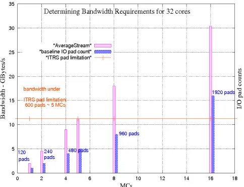
To understand the bandwidth requirements of a likely 32-core system, a bandwidth characterization is proposed. In this characterization, in order to guarantee that addresses are equally distributed along the ranks so that any advantage is taken on locality[17], the most conservative addressing mode is adopted by interleaving cache lines along the RFMCs and closed page mode (server) employed in all experiments.
Fig. 2: determining bandwidth demands and pad requirements to reach core:MC ratio of 32:16
and pin count in both of them. A detailed list of the parameters used in these experiments can be found in Table IIIa.
The rank selected to perform the bandwidth characterization (i) scaling is a generic 1GB-DDR3 DIMM, with 64-data-bit, 1333 MT/s-data-rate, based on Micron MT41K128M8[2] (Ta-ble IIIa). MCs are individually connected to independent ranks to extract their maximum bandwidth. In this characterization, two experiments are performed: in (i), core:MC ratio adopted is 1:1 and this baseline system is modeled as a set of one core/MC/crossbar/selected rank (settings in Table IIIa) using M5[18] and DRAMsim[17] simulators whilst bandwidth is measured utilizing an average of STREAM[19] benchmarks. This experimentation reports a 2.5 GBytes/s-bandwidth, which confirms its proper calibration and validity, since it fits within the bandwidth magnitude range reported by Micron[2].
Experiment (ii) starts with determining the number of pins employed on each rank: as a first observation, in a regular chip, 50% of the total pads are destined to power purposes whilst the other 50% are destined to the remaining signals. Further investigation of Micron manuals[2] shows that 50% of 240 pins available, i.e., around 120 pads, are dedicated to control/data signals, whilst the rest are dedicated to power.
To estimate the maximum number of MCs that fit on the on-package area, Marino’s assumptions[16] are utilized: 16 ranks dies can be fit within the package area and each rank is connected to a different MC (thus 16MCs) so that bandwidth of each rank can be fully explored. Therefore, by employing the previously assumed 32 cores, the core:MC ratio is 32:16.
The same simulators and benchmark suite in (i) are used in (ii), but using 32:16 core:MC ratio rather than the 1:1 core:MC one, as well as scaling pads counts linearly with MC counts. The results of this scaling are reported in Figure 2, where it is observed that 1920 pads (or 3840 pins using the same pad:pin of 1:2 previous assumed proportion) are needed to achieve 32:16 core:MC ratio – 30.4GB/s-bandwidth, which corresponds to a significant larger amount than the ITRS upper limit of 1023 pads [3]. These findings show that when comparing the
maximum bandwidth obtained for core:MC ratio of 32:16 to the baseline (which has core:MC ratio of 32:5), a significant larger bandwidth improvement factor of 2.7x (30.4GB/s over 11.25GB/s) is obtained. As a conclusion, larger MC-counts significantly benefit bandwidth, which motivates the search for pin-scalable solutions.
B. Background: Current memory solutions do not scale
The main focus of current commercial solutions [2] consists of maximizing memory bandwidth by generally increasing the frequency and/or the width of the bus that connects MC to the rank, whilst keeping MC counts at lower magnitudes due to pin restrictions. To start to understand how commercial strategies employ current design parameters, we begin with:
bsr=memory bus width∗f req multiplier∗f req (1)
where bsr represents the maximum bandwidth supplied by the rank, memorybuswidth the width of the memory bus, f req multiplier the bus frequency multiplier, and f req the frequency of the memory bus. For a pad, we define:
bpp=bsr/number of available iopads (2)
where bpp is the bandwidth per pad and
number of available iopads the number of available I/O pads.
As previous experiments have illustrated, current DDR3 memories present around 180-240 I/O pins/MC [2], which are clearly not scalable. Furthermore, using equation 2 with the significant magnitude range of 32-55 pin-range to represent a large amount of pins as in commercial solutions (e.g. Intel FBDIMM[6] with 48 pins/MC and 2.5 Gbits/s/pin; RAMBUS XDR2[8] with 32 pins/MC and 12.8 Gbits/s/pin, HMC[7] with 55 pins/MC and 10 Gbits/s/pin; typical DDR ranks[2] with 123 MC pins and 1.2-5 Gbits/s/pin), lower bandwidth-per-pin rates are obtained, which still remain a challenge when more bandwidth is required, thus motivating the search for pad/pin-scalable solutions.
C. Mechanisms to Achieve Pin/Pad Scalability: optics and RF
In this section, the trade-offs involved when adopting RF/optical technologies to approach pin/pad scalability are explained via modeling modulation signaling principles.
In both RF and optics, high MC scalability can be obtained via modulation combined to very low latencies (light or high-frequency speed transmission) respectively over electrical wires or fiber. Equation 1 is modified to estimate the benefits of modulation. Usingtotal data rateor tdrresults in:
tdr=number carriers∗data rate per carrier (3)
bpp=tdr/number of available iopads (4)
where number carriersalso represents the number of wave-lengths when optical systems are referred. For example, optical Corona [10] is reported to have 2 I/O optical-pins, i.e., 2 optical fibers between MC and the ranks, thus scalable. In this case, equation 4 applied in Corona [10] indicates that:
bpp= 160GBytes/s/2pin= 640GBits/s/pin, (5)
RF technology (nm) 45 32 22
carriers 10 12 14
data rate per band (Gbits/s) 7 8 10
total data rate per wire(Gbits/s) 70 96 140
Max CMOS RF carrier freq(GHz) 592 768 944
space between carriers(GHz) 28 32 36
power (mW) 60 72 84
energy per bit(pJ/bit) 0.85 0.75 0.6
area (TX + RX) (mm2) 0.0115 0.0119 0.0123
[image:5.612.57.291.53.178.2]area/(data rate) (um2)/Gbits/s 164 124 88
TABLE I: RF-interconnection replicated from [12] when modeling RF technology and from ITRS[3]
rates using a low amount of wires/pads-counts. Next, an RF background and modeling are provided to understand the RF behaviour of the RFpads.
D. RF background for RFpads
To facilitate understanding RFpads RF behavior, a simple modeling by Liu [15] is adopted. In this model, the charac-teristic impedance of a QP line is defined as Z0, when the load impedance Zl is different from Z0. Having a wave at the termination reflected to the generator enables to define the reflection coefficient at the termination (γ(l)) as the ratio of the reflected wave to the incident wave the following way:
γ(l)l=V0 +/V0−, or (6) γ(l) = (Zl−Z0)/(Zl+Z0) (7) where V0+is the incident wave amplitude atz= 0, andV0−
the amplitude reflected to the load. Return loss (RL) is defined as available power at the transmission line that will not be delivered thoroughly to the load, and represented (dB) as:
RL= 20.logγ(l)dB, or (8) RL= 20.log(S11)dB (9) Given that the reflection coefficient γ(l) at a distance l from the load can be expressed as:
γ(l) =γ(l).exp(2.j.β.l).exp(2.α.l) =γ(l).exp(2.γ.l) (10) Then, input impedance Zin can be defined as:
Zin=V(l)/I(−l) =Z0.(Zl+Z0.tanhγ.l)/(Z0+Zl.tanhγ.l) (11) where V(−l),I(−l),Z0 andZl are respectively the voltage, current at distance l from the load, impedances at distance 0 and l. With those, the power delivered (Pin) to the transmission line at z = -l can be represented as:
P in=⌊V(−l).I(−l)⌋=|V o+|2)/2Z0.⌈1−γ(l)2⌉.exp(2.α.l) (12) and the power loss through the transmission line can be defined as the difference between P inandP l, represented as:
P loss=P in−P l=|V0+|2
/(2Z0).2.⌈(exp(2.α.l)−1) +γ(l)2
.
(1−exp(−2.α.l)⌉ (13)
Defining reflection coefficient at the source (γg) andZ0 as:
γg= (Zg−Z0)/(Zg+Z0)and (14) Zo2=Zr.⌈[(1 +S11)2−S212]/[(1−S11)−S21]⌉ (15)
insertion loss (IL) can then be defined as the ratio of power of the load to the power from the generator:
IL= 20.log(S21)dB (16) Alternatively, as defined by Liu[15], using a symmetric general two-port transmission line from port 1 (if a simple imaginary line considers port 1 to the left of port 2, atV1 voltage,V1+ direction to the right,V1- signal direction to the left) to port 2 (atV2 voltage, to the right of port 1,V2+ signal direction to the left, andV2−signal direction to the right),S11and S21 parameters, can be defined as:
S11 =V1−/V1 +withV2+ = 0
S21 =V2−/V1 +withV2+ = 0 (17)
In the above model,RLis represented byS11andILbyS21. Very importantly, the previous equations represent a general and simple CPW model. According to Liu[15], it is very challeng-ing to represent and quantify QP lines parameters uschalleng-ing closed equations such as those exemplified previously due to CPW frequency-dependent parameters and complex discontinuities between different parts of its structures, especially at high bandwidth (BW).
To approach these challenges in QP[15], Ansoft HFSS 3D electromagnetic field solver simulator[20] was adopted to de-termineRL(S11),IL(S21)and crosstalk noise (CN) of a QP CPW. In the report[15], Liu performed a very wide range of CPW simulations with different widths (100µm, 50µm, 20µm and 10µm), different silicon substrate resistivities and a wide range of BW: 0 to 40GHz for (100µm and 50µm) and 0 to 200GHz for (20µm and 10µm).
Furthermore, besides RLandIL, crosstalk (CN) was also investigated by Liu[15]. By simulating with several ground-lane configurations between QP lines, Liu[15] shows that isolation between different QP lines is improved.
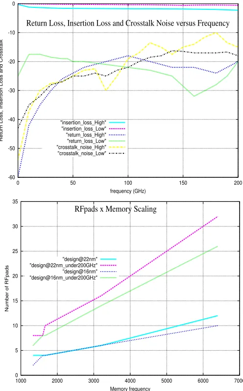
As a result, many different curves of RL, IL and CN were obtained for a wide variety of frequencies. While Figure 4a illustates obtained RL, IL and CN, these parameters proportionally increase with the increase of the frequency. RF behavior is further approached in Section IV-B.
III. RF iop
In this section, RF iop memory organization techniques explore RFpad scalability which enables RFMC scalability. In order to have I/O pin counts minimized to achieve RFMC scalability, memory channels are best matched with RF. Whilst minimizing I/O pin counts of each individual MC, the total pin count must be scalable targeting bandwidth increase as well as keeping power utilization within low levels.
A. RF iop Overview and General Design rules
A general view ofRF iopcan be found in Figure 3.RF iop employs the following strategies: (1) minimal amount of ele-ments designed for RF and also (2) for short distances.
control bits
control bits MC
DRAM rank
..
.
RFpaddata transmission line quilt−packaging interconnection control transmission line
quilt−packaging interconnection RFpad
control in control out
data out
DRAM banks
data in
data bits
data bits
data out
data buffer out
data buffer in
processing engine transaction
engine front end
cache line request (address)
cache line
TX RX
TX
RX
RX
RX TX
[image:6.612.44.298.54.274.2]TX
Fig. 3: RF iopscheme [16].
processor die, (2) off-die RF-interconnection lines, and (3) by on-package ranks placed on the rank dies in a coplanar fashion. In each RFMC, RF TX/RX are responsible for mod-ulating/demodulating data/commands. Modulated signals (RF waves) are transmitted/received through the RF QP lines. To address RF-transmission challenges, lesser elements such as RF TX/RX at the RFMCs, RFpads (QP) and ranks are employed when compared to typical solutions [21].
Furthermore, the fact that inRF iopall elements are properly designed for RF minimizes the previously mentioned RF degra-dation effects (RL,ILandCN). The short distances employed in RF iop can be traversed through QP lines which connect the RFMCs to ranks and allow significantly lower degradation effects than those along long printed-circuit-board (PCB) as reported in [22].
B. Ranks manufactured as dies and rank width
Before other new technologies such as HMC[7] were de-veloped, RF iop employed ranks manufactured as DDR dies, each die containing its proper set of TX/RX to be able to communicate with the RFMCs (at the processor die). InRF iop, the fact that ranks operate as traditional DDR elements allows compatibility with memories in the market, thus not requiring any protocol or memory timing change. In Figure 1, a memory die with its RF TX/RX is connected to the core (with its RFMCs, i.e., MCs coupled to RF TX/RX). To keep DDR compatibility along future DDR-memory generations, RF iop employs typical DDR-rank width, i.e., 64 bits (8 Bytes) [2]. The width aspect is further discussed.
C. RF iopsignal path
In Figure 3, the interface between the TX/RX elements and MC (to form an RFMC) and the RFpads is illustrated: TXs/RXs are assumed to be present on each RFMC and rank, and upon a cache request, signals go through the RFMC TX
where they are converted to analog waves. Next they traverse the waveguide/CPW and reach RX, where analog waves are converted back to digital signals in order to reach the busses and a rank. The signal does traverse the same path in the opposite direction when a rank responds, and at the RFMC-RX it is converted down back to digital before reaching the processor.
D. RF iopViability
RF iop viability relies on QP lines. The fact that QP was prototyped and tested forBW up to 60GHz, whilst presenting low-magnitude return loss (0.1dB), demonstrates the viability of RFpads. Moreover, being simulated forBW up to 200GHz, QP lines reduce the number of pads, which is aligned to the pad reduction goals.
In general, RF design explores the matureness achieved in CMOS manufacturing, and is therefore a very consolidated technology. Once putting chips down and sliding to match each other is a straightforward process according to [15], QP lines are reported to be manufacturable through the programmability of already-existing industry tools such as pattern-recognition of the modules. Self-alignment structures are easily built into the shapes of the nodules as indicated in [15]. Deep reactive ion etching (DRIE) can be used to separate chips from wafers.
E. RF iop Limitations and Approaches to address them
The following approaches address the previously mentioned RF ioplimitations:
• The manufacturing technology evolution is likely to allow a reduction of twice the area used by the cores, thus likely allowing more ranks to be fit, which enables a large core:package area ratio.
• Other than using QP as RF-interconnection lines in
RF iop, microstrips and striplines could be potentially em-ployed [12] thus allowing other benefits such as lowering costs, improving data rates, and/or reducing losses.
IV. EXPERIMENTALSECTION
Bandwidth, latency, number of pads, energy, area and temper-ature are the key technical elements which help the researcher understand the goals and achievements ofRF iop. To evaluate these RF iop elements, an experimental infrastructure com-posed by Mathematical modeling and several detailed-accurate simulators is employed as follows:
• Determination of QP RF BW ranges needed to match memory data rates to minimize the number of RFpads.
• To the best of our knowledge, it is the first time that a Mathematical modeling for IL,RLandCN is obtained via regression from the resulting RF-behavioural simula-tions performed by Liu [15].
• Mathematical pad scaling modeling to determine the be-haviour of the number of RFpads as a function of the rank data rates and width.
• M5 simulator [18] to simulate the multicore system run-ning bandwidth-bound applications.
requests generated by the M5 simulator. After having sim-ulated these transactions, DRAMsim returns the answers of the requests to M5. Rank power statistics are collected from DRAMsim and/or Micron power sheet [2].
• Cacti [23] cache simulator to determine cache latencies to be used in M5 multicore simulation.
• McPAT [24] simulator collects architectural results from M5 and determines the amount of area and power used by different components of an RFMC.
• Derive power modeling for the RF-based memory channel based on the Mathematical modeling developed in [14]. • Temperature simulation [25] to determine the behaviour
ofRF iopmemory organization.
The first three steps previously proposed guide the RFpads behavioural modeling in terms of RF behaviour and scaling. The remaining steps allow to extract performance, power and temperature implications ofRF iop.
A. Determination of RF frequency ranges to match memory data rates
In the first order, bandwidth provided by each rank dictates the number of lines required: not considering loss effects, the ratio between rank bandwidth and RFpad RF-bandwidth determines the amount of RFpads needed to match rank data rate.
To show the benefits of an RF-based memory path, once QP was manufactured and has validated RF-properties, QP lines/parameters are employed as the RF-interconnection lines between RFMCs/ranks inRF iopwithout any loss in generality. To determine the number of RFpads (RFpad counts), the number of QP lines is required: the key is to match QP data rate to the rank data rate. QP data rates are estimated with on-chip RF scaling predictions by F. Chang et al. [12] (Table Ib). Though valid for on-chip interconnections, these are also considered valid when connecting two different dies via QP. A second reason to justify this strategy is the significantly reduced inter-die distance in QP (around 40um), completely within on-chip typical distance ranges. RFpad count determination is performed under three strategies: (i) considering simulated QP BW (200GHz [15]), (ii) validated QPBW (60GHz [15]), and (iii) taking into account just RF predictions (half of maximum CMOS frequency carrier in table I[3][12]) i.e., regardless of the assumption of QP as RFpads.
In strategy (i), design and estimation of RFpads counts em-ploy the rank previously used in Section II. 32nm-technology is assumed - in Table Ib; it allows 12 carriers and data rate per carrier of 8Gbits/s. With a static RF band allocation [12] these carriers are spaced by 32GHz to avoid crosstalk (further described) that could lead to low bit error rate (BER). Using QPBW as 200GHz[15] and previous carrier spacing, there are up to 6 carriers, each with 8Gbits/s of data rate, thus the overall data rate budget available for each RFMC is 48 Gbits/s. Next, importantRL,IL andCN parameters are determined.
B. Determination of Return Loss (RL), Insertion Loss (IL)
and Crosstalk Noise (CN) for RFpads
As mentioned in Section II-D, Liu [15] has performed a wide range of simulations using Ansoft HFSS 3D electromag-netic field solver simulator [20] in order to determineRL(S11), IL(S21)and CN behaviour of the RFpads. In these simula-tions, different RFpad widths and different silicon resistivity substrate for a wide range of frequencies were utilized. To exemplify, the widths (100µm, 50µm, 20µm and 10µm), and two different silicon resistivity substrates (high, which means a magnitude resistivity of 8000Ω.cm and low, which means a resistivity magnitude of 10Ω.cm) as well as BW from 0 to 40GHz for (100µm- and 50µm-width) and from 0 to 200GHz for (20µm- and 10µm-width) were simulated.
Output magnitudes of these previously simulated losses for the 20um-width RFpad are illustrated in Figure 4a. In this example IL is lower than -5dB, RL stays between -20 and -40dB andCN between -60 and -10dB. If such losses are not acceptable, it is a designer’s task to tackle them, such as having larger separation gaps between them or augmenting the number RFpads.
In order to incorporate the behaviour of the RF circuits in the RFpads RL, IL and CN parameters are proposed to be represented via an extensive least square quadratic polynomial regression over the wide range ofIL,RLandCN simulations performed in [15] in order to determine their Mathematical behaviours as a function of frequency ranges within BW. Without any loss in generality, given simulated BW magni-tudes of 200GHz, the 20µm-width range and high resistivity are conservatively adopted. As a result of this regression, the following formulations are obtained:
RLH(f) = 2.573988065∗10−16∗f9−2.22139361∗10−13∗f8+
= 8.020049855∗10−11∗f7−1.576525975∗10−8∗f6+
= 1.843388408∗10−6∗f5−1.320228749∗10−4∗f4+
= 5.797660813∗10−3∗f3−1.566649281∗10−1∗f2+
= 2.882054915∗f−59.96827969
(18)
ILH(f) = 2.459007338∗10−19∗f10−2.469419009∗10−16∗f9+
= 1.062082119∗10−13∗f8−2.556564595∗10−11∗f7+
= 3.777876047∗10−9f6−3.538827666∗10−7∗f5+
= 2.098085852∗10−5∗f47.660830361∗10−4f3+
= 1.64219124∗10−2∗f2−1.995163588∗10−1∗f−
= 2.526135981∗10−1
(19)
CN H(f) =s13 =−1.567317848∗10−18∗f10+
= 1.678387101∗10−15∗f9−7.774761181∗10−13∗f8+
= 2.039691044∗10−10∗f7−3.330113718∗10−8f6+
= 3.49673987∗10−6∗f5−2.355209243∗10−4f4+
= 9.886149607∗10−3∗f3−2.484417801∗10−1∗f2+
= 3.633086388∗f−47.08822923
and CN H means crosstalk noise, all at high resistivity. By performing the previous regression, it is guaranteed thatRL,IL andCN follow the simulations performed, i.e., to include RF behavioural details in the RFpads. Given the above equations, the designer can determine the behaviour of such important RF parameters (IL, RL and CN) for future memory data rates. Other equations such as return loss (RLL), insertion loss (ILL) or crosstalk noise at low resistivity (CN Lor s13), can be similarly obtained and are omitted due to lack of space.
C. Determination of the Number of RFpads
For subsequent modeling, memory read/write operations are assumed, while utilizing RFpad modeling equations (from equation 21 to 27 developed in Marino’s report [16].
RF-delays through TX/RX are not included in the following formulations due to their insignificant magnitudes (around 200-picosecond range [12]) compared to the duration of mem-ory timing operations. To determine RFpad count behaviour, memory bitsormbis defined as:
mb=mc∗dr (21)
i.e., a function of the number of bits transmitted in one memory cycle -mc, wheredr is the memory data rate. RF ioptotal cycle (tot cycle) is limited by the maximum BW allowed in QP (200 GHz [15] as QP is adopted). Keeping DRAM circuitry as original as possible, dedicated RF-interconnection lines (control and data) for RFpads are included:
RF pads=number of RF pads per RF M C (22) RF pads data=f loor(data mb/(mc∗mb)) (23) RF pads data=f loor(data mb/(mc∗drRF c∗nRF c))
(24) Considering respectively RF paddr, RF pads data, RF pads ct, drRF c, nRF c as the total RFpad data rate, number of RFpads destined for data/control lines, data rate carriers, and number of RF carriers, the following equations can be utilized:
RF iopaddr=XnRF c∗drRF c, (25) RF pads ct=f loor(ct mb/(mc∗drRF c∗nRF c)) (26) RF pads=RF line data+RF line ct (27) Having inspected ranks with similar features in Micron catalogs [2], except voltage, ground, and not-connected pins, around 123 bits are used in one rank access (total of 240 pins, around 50%; 64 for data, and 59 for control). Assum-ing the same rank (1GB-DIMM DDR3 rank, with 64-data-bit, 1333 MT/s-data-rate, based on Micron MT41K128M8[2]) previously employed in the bandwidth characterization (Section II-A), from equations (5,6) the total amount of bits (tot bits) transferred via one RFpad in one memory clock (1/1333MT/s) is:
tot bits= (1/1333/s)∗6carriers∗8Gbits/s; (28) f loor(tot bits) = 36bits, (29) Therefore, in one memory cycle only 4 RFpads are needed to perform an RF transfer of 144 bits, which carry the total of
-60 -50 -40 -30 -20 -10 0
0 50 100 150 200
Return Loss, Insertion Loss and Crosstalk
frequency (GHz)
Return Loss, Insertion Loss and Crosstalk Noise versus Frequency
"insertion_loss_High" "insertion_loss_Low" "return_loss_High" "return_loss_Low" "crosstalk_noise_High" "crosstalk_noise_Low"
0 5 10 15 20 25 30 35
1000 2000 3000 4000 5000 6000 7000
Number of RFpads
Memory frequency
RFpads x Memory Scaling
[image:8.612.315.563.57.455.2]"design@22nm" "design@22nm_under200GHz" "design@16nm" "design@16nm_under200GHz"
Fig. 4: top to bottom: (a) return loss (RL), insertion loss(IL) and crosstalk noise (CN) for high and low resistivity versus BW; (b) RFpad and memory data rates.
123 memory bits (64 of data plus 59 of control). Other widths can be used via recalculation of equations starting from 21.
According to Chang et. al [12], to avoidIL, RL andCN previously observed effects and minimize likely BER, as a general rule-of-thumb RFpads are doubled. Following this rule, 8 RFpads are required to transfer 64-data and 59-control bits.
Very importantly, Figure 4b shows related experiments per-formed in the initialRF iopreport [16]. Comparing Figures 4a and 4b, either with faster DDR3 memories (1333MT/s versus 666MT/s in the initialRF iopreport) or DDR4/DDR5 models, RFpads still scale properly, enabling RFMC scaling.
By comparing RFpad scalability to current DDR-based pad counts, assuming a pad:pin ratio of 1:1 and 200-GHz-BW (QP parameters[15]), it is concluded that RF iophas 4x more MC pads (8 RFpads) than optical-Corona [10], a MC pad reduction of 4x when compared to RAMBUS XDR2, and up to 6x when compared to FBDIMMM.
about HMC is presented. A HMC rank is composed of a single package containing multiple memory dies which form one logic die. A vault is defined as a set of banks of memory dies, and different vaults are going to contain different memory die portions. Each vault has a MC named vault controller (VC) which is responsible for managing its memory references to that specific vault, besides timing, refresh operations, and buffering vault accesses. As opposed to HMC,RF iop follows typical DDR organization in ranks (rows, columns, and banks) as multiple dies placed on a coplanar layout (Figure 1).
In HMC, the communication between memory die and processor happens via serial/deserial communication over I/O-links, whileRF iopemploys modulation over QP lines. Typical I/O-links in HMC present 10Gbit/s versus 48Gbit/s-links (6 carriers, 8Gbits/s data rate) in RF iop. The maximum aggre-gated bandwidth in HMC is 320GB/s, which is significantly higher than in RF iop, i.e., with memory settings defined in section II.A, RF iop maximum bandwidth achieves 96 GB/s (16RFMCs x 6GB/s). However, to have RF iop achieving the same levels of bandwidth of HMC the improvement of transistor technology is likely to allow (i) a larger number of RFMCs (1:1 RFMC:rank assumption); (ii) QP BW is likely to increase. Assuming that at 22nm, 32 ranks can be fit in (i) RF iop package area, RF iopmemory bandwidth is leveraged to 192GB/s. (ii) With the assumption that the QP BW is doubled, about double the carriers can be fit whilst larger data rates are allowed (10Gbits/s) thus resulting in 480GB/s, which is much larger than 320GB/s in HMC.
Alternatively, if the number of pads is not considered, having the 55 pins of HMC (versus 4RFpads in RF iop) as budget in RF iopallows 1056GB/s (55 over 4 = 11; 96GB/s * 11 = 1056), i.e., 3x more bandwidth than HMC. Further advancing RF iop report[16], assuming a pad:pin ratio of 1:2 (at the beginning of this subsection) and that a HMC memory package utilizes 8 links correspondent to 8 VCs and 55 I/O-pins, in RF iop the equivalent configuration with 8 RFMCs - each RFMC corresponding to one VC - is likely to have 32 RFpads, i.e., a much lower pad usage than HMC.
To predict future memory data rate versus RFpads scaling behaviour (which is supported by the scaling of RF technology, number of carriers andBW) different types of faster memories (e.g. DDR4/DDR5) are similarly modeled (via equations 4/6) (i) with and (ii) without a BW limit of 200GHz (QP [15]) and using 16nm-/22nm-RF-technology based on RF ITRS predictions [3][12]. The result of this modeling is shown in Figure 4b, which demonstrates RFpad scalability along future memory and RF interconnection generations.
On strategy (ii) (defined at Subsection IV-C) as assumed in RFiop report [16], a combination of QP prototyped/validated BW of 60 GHz [15] with the pad reductions obtained (30% in RAMBUS XDR2 and 50% in Intel FBDIMM), it is found that, if compared to HMC, RF iop can reduce the number of pads up to about 56%.
Moreover, regarding strategy (iii) which was defined at Sub-section IV-C, assuming RF predictions [3][12] and disregarding
tech MC I/O bandwidth intercon. mem
pad per pin energy energy
count (Gbits/s/pin) per pin (pJ/bit)
GDDR5 120 2.5 - 250
DDR3 120 1.6 8 160
1600
DDR4/ 120 5 - 250
DDR5
-Intel 48 2.5 -
-FBDIMM -
-RAMBUS 32 12.8 - 50
XDR2
-HMC 55 10.0 - 100
[7]
Optical 2 640 0.078
-Corona
DIMM 39 8 2.5-4
-Tree
[image:9.612.335.545.51.287.2]-RF iop 8 6-12 0.6-0.7 87
TABLE II: different memory systems comparison: number of I/O pads, memory bandwidth per pin, interconnection energy, and memory energy [2][6][8][10][12][26]
QP parameters, remarkable 4RFpads are found as reported in [16], which are of similar magnitude to optical-Corona [10].
Table II compares pad-count, bandwidth-per-pin, intercon-nection energy, and energy among diverse systems, including RF iop. Other energy aspects are discussed in subsection IV-I. Comparing modeling equations 22-27 to the ones previously developed in [16]:
• equations 21-27 are valid for different types: different data rates and/or widths than 8 bytes (DDR standard). • equations 21-27 can be used to determine different pad
counts as a function of scaling widths.
Next, different memory types/technology and RFpad counts scalings are compared using the developed modeling.
D. RFpad area. Die area saving and I/O pad reduction
Liu’s design space exploration [15] of QP dimensions results in 20µm-to-100µm and 10µm respectively for depth and width. Since QP lines are RFpads, previously obtained dimensions are valid for RFpads. Using these results, Marino [16] reports RFpad dimensions of 200µm2 to 1000µm2. Once the insertion
of ground lines is the typical rule of thumb to minimize crosstalk between two adjacent lines, RFpad pitch is conser-vatively assumed as the largest dimension of QP, i.e., around 100µm.
pads can be potentially saved [21]. Furthermore, since I/O pads are connected to the same set of I/O pins, a significant reduction is expected in the latter[21]. A comparative area analysis between RFMC and traditional MC is performed in Subsection IV-H. Next, temperature comparison with 3DStack-ing is approached.
E. Temperature Comparison:RF iop and 3Dstacking
In this subsection temperature effects are compared inRF iop and 3Dstacking when scaling ranks. Both architectures are assumed to have: (i) 256um2for rank area based on 3Dstacking rank dimensions [1] once 3Dstacking is an on-package/on-die technology; (ii) initial rank temperatures at the same magnitude of the L2 caches (assumed as 60 degree Celsius).
(iii) Hotspot tool [25] with its respective gcc benchmark trace is used to compare both architectures. (iv) Most parameters employed in this estimation are the default ones used in the Hotspot tool configuration file [25], except the area covered by the heat sink and spreader, which is conservatively adjusted to a maximum of 0.05m in either configurations.
(iv) The number of ranks was scaled up to 16, either in RF iop/3Dstacking to match the maximum number of RFMCs/MCs. As a result of this temperature modeling,RF iop is about 10.5% lower than 3Dstacking, thus likely to be advantageous when scaling of ranks/RFMCs.
F. Performance Evaluation Methodology
RF iopis modeled using M5 [18] and DRAMsim [17] simu-lators. Memory transactions are generated by M5 and captured by multiple MCs/RFMCs in DRAMsim, which responds to M5 with the result of the memory transaction. To have enough memory pressure and demonstrate higher bandwidth under RFMC scalability, a clustered microprocessor architecture with 32 cores is selected - previously explained in the motivation section - versus 16 cores in previousRF iopreport [16]. Fur-thermore, to ensure higher memory pressure OOO-processors (based on Alpha, 4-wide issue, similar as in [16]) have been employed with private L2 slices to prevent cache sharing from affecting bandwidth. Furthermore, a banked-scalable L2 MSHR structure is assumed with 1MB/core L2 slice size [27]. L2 slices communicate through an 1-cycle RF-crossbar, i.e., similar RF-circuitry latency settings adopted by F. Chang et al. [12]: 200ps of TX-RX delay, plus the rest of the cycle to transfer 64 Bytes via high speed/modulation, which also prevents larger interconnection delays from masking memory settings. Instead of bus delays, RF TX-RX delays were also configured in DRAMsim to represent RF transmission.
Based on the rank previously used in Section II (Micron MT41K128M8 [2], parameters in Table IIIb are kept constant throughout all experiments). To generalizeRF iop usage with different DDR-families, different rank parameter settings from [16] are used, particularly with the 1333MT/s-memory data rate instead of the 666MT/s.
In all experiments, as stated in Section II-A, to avoid no advantage is taken on locality, [17] addresses are equally distributed along the ranks, via cache-address interleaving along
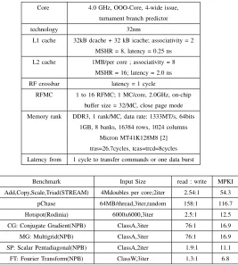
Core 4.0 GHz, OOO-Core, 4-wide issue,
turnament branch predictor
technology 32nm
L1 cache 32kB dcache + 32 kB icache; associativity = 2
MSHR = 8, latency = 0.25 ns
L2 cache 1MB/per core ; associativity = 8
MSHR = 16; latency = 2.0 ns
RF crossbar latency = 1 cycle
RFMC 1 to 16 RFMC; 1 MC/core, 2.0GHz, on-chip
buffer size = 32/MC, close page mode
Memory rank DDR3, 1 rank/MC, data rate: 1333MT/s, 64bits
1GB, 8 banks, 16384 rows, 1024 columns
Micron MT41K128M8 [2]
tras=26.7cycles, tcas=trcd=8cycles
Latency from 1 cycle to transfer commands or one data burst
Benchmark Input Size read : write MPKI
Add,Copy,Scale,Triad(STREAM) 4Mdoubles per core;2iter 2.54:1 54.3
pChase 64MB/thread,3iter,random 158:1 116.7
Hotspot(Rodinia) 6000x6000,3iter 2.5:1 12.5
CG: Conjugate Gradient(NPB) ClassA,3iter 76:1 16.9
MG: Multigrid(NPB) ClassA,3iter 76:1 16.9
SP: Scalar Pentadiagonal(NPB) ClassA,2iter 1.9:1 11.1
[image:10.612.317.584.52.349.2]FT: Fourier Transform(NPB) ClassW,3iter 1.3:1 6.8
TABLE III: top: (a) Parameters of the modeled architecture; bottom: (b) benchmarks configuration.
RFMCs and closed page mode (server). Using previous RF assumptions, a 200ps-TX/RX-delay[12] is estimated. Due to the speed-of-light property of RF, signal delays of commands-duration and burst-commands-duration between RFMC/rank are estimated to be reduced from two cycles to one cycle and from eight cycles (typical) to one cycle[2]. DRAMsim was modified to support an arbitrary number of RFMCs. In DRAMsim, each RFMC has a FIFO associated to queue memory requests, as well as duration and occupation of the banks and taking all of these into consideration contention is properly modeled. To evaluate RFMC scalability, core:MC proportion is varied from the baseline configuration 32:5 up to 32:16 (32 cores, 16 RFMCs, as previously justified) via M5/DRAMsim simulations with a different number of RFMCs. In Figures 5a and 5b, the baseline core:MC ratio of 32:5 is shown as a matter of reference - 5MCs (Section II-A).
To obtain cache latencies, Cacti[23] is set with aggressive ultra low-power optimizations. MSHR counts selected for each L2 slice follow the study by Loh[1] once multiple MCs and ranks as OOO-cores are used in it. Summarizing, all parameters used in the simulation environment are in Table IIIa.
Hotspot from Rodinia suite[29]; (iv) Conjugate Gradient (CG), Scalar Pentadiagonal (SP) and Fourier Transform (FT), from NPB as part of the HPC challenge to evaluate bandwidth[30]. STREAM and pChase bandwidth measurements are extracted from these applications since these are designed to measure bandwidth. Table IIIb shows the benchmarks, input sizes, read-to-write rate, and L2 MPKI obtained. In all benchmarks, parallel regions of interest are executed until completion. Input sizes are large enough to stress the memory system (120MB to 1.8GB). Average results are calculated using harmonic average. For the rest of this evaluation, the following are defined:
• baseline: as determined in section II, corresponding to the electrical counterpart version with 5 MCs (Section 2), which are constrained to I/O pin scalability.
• RF iop: representsRF iopwith RFMC scalability benefits, i.e., with RFMCs scaling up to 16 RFMCs and 16 ranks. • To facilitate comparison, the terms RF iopa,
RF iop burst command andRF iopa burst command are adopted from Marino’s report[16].RF iopa is defined as the RF version with the same area budget as the baseline to explore its architectural benefits in terms of higher RFMC counts. As further described in Section IV-H, RF iopa can have up to 12 RFMCs.RF iopa magnitudes were not directly obtained from the simulators, but extrapolated from the performance results.
• RF iop burst command:RF iopplus (simultaneously) RF latency benefits (on command/burst transfers).
• RF iopa burst command:RF iopa plus RF latency bene-fits applied to command and burst transfers.
• RF iopp: as the version that uses MC power as power budget, based on further power/energy analysis (Subsec-tion IV-I1),RF iopp can have up to 16 RFMCs.RF iopp has bandwidth/speedup behaviour similar toRF iop.
G. Bandwidth, Latency, Speedups and Number of cores: Sen-sitive Analysis
Bandwidth benefits from RFMC scalability are analysed first, and next high-speed signaling. In Figure 5a, the bandwidth obtained for different core:MC ratios (32:5, 32:8, 32:12 and 32:16), and with STREAM and pChase, respectively represent-ing stream and random behaviours is improved with the in-crease of the number of RFMCs. Significantly,RF iop/RF iopa respectively provide 3.6x and 2.6x more bandwidth than the baseline due to larger RFMC counts (larger memory paral-lelism). Comparing Figures 5a and 6, bandwidths are up to 10% larger due to the use of larger data rate memories. More-over, RFMC scalability does provide bandwidth growth with different memory settings and any number of RFMCs, which generalizes and validates RF iop RFMC scaling previously proposed[16].
Speedups obtained for different core:MC ratio (32:5, 32:8, 32:12, and 32:16), i.e. with different RFMC counts, are shown in Figure 5b. For all benchmarks, speedups increase propor-tionally to the increase of the number of RFMCs. Compared to the baseline, for STREAM benchmarkRF iop andRF iopa are 4x and 3x significantly faster. Similar significant scaling
trends are obtained of 2.4x for pChase, 3x for Hotspot, 2.3x faster for CG, 2.2x for FFT, 2.7 for SP, and 2.5x for MG. The largest bandwidth and speedup improvements occur for STREAM and pChase due to their large MPKI magnitudes (Table IIIb). Significant results using this variety of bandwidth-bound benchmarks demonstrate the generality of the solution.
Considering RFMC scalability, pChase bandwidth and la-tency present improvements of 4%-25.8% and 10%, whilst speedups improve up to 3x (transaction queue average dura-tion/occupancy reduction). Combining RFMC scalability and high-speed, overall speedups have shown a significant improve-ment of up to 4.3x, whilst RF iopa achieved a significant factor of 3.2x when compared to the baseline. Alternatively, the latency in Figure 8 follows a similar reduction trend when considering high-speed RF benefits.
RF iopa (RF iop under area budget constraints) presents similar behaviour trends to RF iop for bandwidth, speedups, and latency. Therefore, performance and energy benefits can be observed when architectural area benefits of RFMCs replacing traditional MCs (RF iopa definition) are considered.
Similarly toRF iopa, architectural power budget is explored by replacing traditional MCs with RFMCs inRF iopp. Archi-tectural area (Section IV-H) and power (Section IV-I) analyses show that a larger number of RFMCs can be used inRF iopp (16 RFMCs) than inRF iopa (12 RFMCs). This demonstrates that the area factor considered in RF iopa is more restrictive than the power factor considered inRF iopp, whilst bandwidths and speedups are achieved in both.
Whilst some benchmarks exhibit RFMC scalability limita-tion (observed saturalimita-tion on the bandwidth/speedup curves), considering that memory requests are equally interleaved over RFMCs and cache transfers are done in one cycle (RF-crossbar latency), a deeper investigation of simulators statistics shows significantly different L2 miss rates in some slices, which provides evidence of the churn phenomenon reported by Loh [1] when scaling MSHRs, not necessarily decreasing L2 miss rates, that is left as a further investigation [16]. Moreover, Figure 5b presents speedups 10% higher than in Figure 6, thus demonstrating that benefits provided by a larger number of RFMCS are also valid for different benchmarks. A sensitivity analysis of the number of cores and latency is performed next.
1) Number of Cores: More cores in the experiments shown
in Figure 5 (32 cores) than in previously published results shown in Figure 6 (16 cores) illustrate that higher MC counts improve bandwidths/speedups inRF iop/RF iopa up to 20%.
2) Latency: Larger RFMC availability results on shallower
0 0.5 1 1.5 2 2.5 3 3.5 4 4.5
5 8 12 16 5 8 12 16 5 8 12 16 5 8 12 16 5 8 12 16 5 8 12 16 5 8 12 16
Bandwidth, Occupancy, Duration: normalized to the baseline (x times)
number of MCs
32 cores
RFiop RFiop_burst_command RFiopa (12 RFMCs) RFiopa_burst_command (12 RFMCs) "baseline (5 MCs)" Add
Copy
Scale
Triad
pChase
occupation duration
Bandwidth
0 0.5 1 1.5 2 2.5 3 3.5 4 4.5
5 8 12 16 5 8 12 16 5 8 12 16 5 8 12 16 5 8 12 16 5 8 12 16 5 8 12 16 5 8 12 16 5 8 12 16 5 8 12 16
Speedup normalized to the baseline (x times)
number of MCs
Speedup Normalized to the baseline - 32 cores RFiop RFiop_burst_command RFiopa (12 RFMCs) RFiopa_burst_command (12 RFMCs) "baseline (5 MCs)"
Add Copy
Scale
Triad
pChase Hotspot
CG
FT SP
[image:12.612.61.556.59.281.2]MG
Fig. 5: 32 cores; left to right (a): bandwidth, tr. queue occupancy/duration; (b): speedups; baseline: I/O pad constraints;RF iop: RFMCs/RFpads;RF iopa/RF iopp:RF iopunder area/power budget;RF iopa/p burst commands: plus RF latency benefits
0 0.5 1 1.5 2 2.5 3 3.5 4 4.5 5
1 2 4 8 9 16 1 2 4 8 9 16 1 2 4 8 9 16 1 2 4 8 9 16 1 2 4 8 9 16 1 2 4 8 9 16 1 2 4 8 9 16 1 2 4 8 9 16 1 2 4 8 9 16 1 2 4 8 9 16 1 2 4 8 9 16 1 2 4 8 9 16 1 2 4 8 9 16 1 2 4 8 9 16
Bandwidth, Speedup, Occupancy, Duration, Latency: normalized (baseline; x times)
number of MCs
RFiop versus baseline - 16 cores RFio
RFioburstcommand
RFa (9 RFMCs) RFaburstcommand (9 RFMCs) baseline (4 MCs)
Add
CopyScale
Triad
pChase
Occupancy Duration pChaseLatency
Bandwidth Speedups
Add
Copy
Scale Triad
pChase
FT
Fig. 6: RF iop, 16 cores from [16]; Left: bandwidth, tr. queue occup/duration; right: speedups; baseline: I/O pad constraint; RF iop: RFMCs/RFpads;RF iopa:RF iopunder area budget;RF iop/RF iopa burst commands;RF iopp/RF iopplus RF latency benefits
those shown in Figure 8, a surprisingly remarkable latency reduction of 30% is obtained. Even when using twice as fast memories, RFMC scalability can further reduce latencies under the pressure of twice the number of cores generating memory traffic. Compared to the previous experiments in Figure 6 where 666MT/s-memories were used, occupancy and duration are lower in Figure 5a with 1333MT/s-memories.
H. RFMC versus MC area
First TX/RX area is estimated and after that, the impact of this area is determined for different technology generations. To estimate TX/RX area, a similar methodology (further described in Subsection IV-I1) is adopted from Tamet al. in [14] as a
combination of RF circuitry area estimations from ITRS[3], de-sign of TX/RX circuitry[12] and validated TX/RX circuits [31]. As a result, TX/RX area is estimated at about 0.0123-0.015 mm2, which is of lower overhead.
[image:12.612.54.551.310.520.2]0 0.5 1 1.5 2 2.5 3
45nm 32nm 22nm
Area (mm2)
technology (nm) Area: MC x RFMC for different technologies
FE TE PHY RF TX/RX MC
RFMC
MC
RFMC
MC
[image:13.612.53.295.55.230.2]RFMC
Fig. 7: RFMC area saving
McPAT[24] tool estimates area and power of FE/TE/PHY parts of a regular MC. Since FE and TE are both present in MC/RFMC, by using an average over the previous simulated benchmarks in McPAT as well as specific RF iop settings (methodology further described in Subsection IV-I1), the area occupied by FE/TE is determined whilst RF RX/TX area are obtained as previously described.
Similar to Marino’s report[16], in Figure 7 it is observed that PHY is the dominant element in terms of area; for different technology generations, 57.3% of MC area can be saved when replacing MCs by RFMCs. Put differently, by adopting MC area as area budget, up to 2.4x more RFMCs can be fit on the die, i.e. up to 12 RFMCs (versus 5MCs-baseline area budget).
I. Power and Energy Analyses
The following analyses aim to identify and compare power/energy magnitudes of RF iop with its respective tra-ditional counterpart: RFpad interconnection and total rank energies.
1) RFpad interconnection energy: As previously analysed
in Subsection IV-H, FE/TE are either present in RFMC or MC and, as previously adopted, McPAT is used to estimate the power of both these parts. However, since the PHY is the most significant element in terms of power when compared to FE and TE, its power and amount of bits transferred to/from memory are included as part of the dynamic energy.
According to the methodologies [8][10][26], energy is prefer-able rather than power since the former considers the amount of bits transferred with the memory. For a traditional MC, PHY contains I/O pins and a regular channel, which power can be estimated by McPAT[24]. However, for RFMC, PHY is represented by RF TX/RX and RF interconnection, i.e., I/O pin and line power is replaced with TX/RX and RF line power.
Similarly to the previous RF TX/RF area estimation in Subsection IV-H, power estimation relies on a combination of RF circuitry estimations from ITRS[3], design of TX/RX circuitry[12], and validated TX/RX circuits [31], all adjusted toRF iopsettings: (i) an average distance of about 1mm from each RFMC to its respective rank RX/TX is assumed ; (ii) since
0 20 40 60 80 100 120
4 6 8 10 12 14 16
pChase Latency (ns)
Number of MCs pChase: measured latency (ns)
baseline latency: 5 MCs latency_RFiop
latency_RFiop_burst_commands
Fig. 8: pChase measured latencies
QPRLis of significantly reduced magnitude [15], and TX/RXs elements designed for QP are still an open area, a conservative power reduction - estimated in 10% - can be applied to the employed transmission models[12][14].
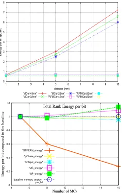
Moreover, since energy-per-bit depends on bandwidth, its modeling is performed considering an average of the sim-ulations performed previously (Subsections IV-F and IV-G), which includes their memory utilization. Figure 9a illustrates the results of energy modeling in which different distances and different technologies (45, 32, and 22nm) are experimented for RF versus traditional ones. Given distances assumed, RF can save an average of 78% of PHY energy if compared to the baseline. This power budget reduction allows the significant factor of 4.6x more RFMCs to be fit in the package area, i.e. a total of 23 RFMCs (5 x 4.6), conservatively rounded to 16 RFMCs (maximum of 16 RFMCs as previously stated [16]).
2) Total Rank Energy: In this work RF iop is set with
traditional DDR3-1333MT/s ranks (detailed in Table IIIa), mainly focusing on the memory channel reduction, rather than on rank power reduction. Despite this, it is also shown that TX/RX utilization at the rank can reduce power which can be estimated by employing Micron power sheet [2], whilst previously assumed RF models [12][14] are employed to es-timate RF TX/RX power. Therefore I/O pin termination power is replaced with TX/RX power inRF iop: this results in a 6.7% power reduction of DRAM power.
In order to determine the total rank energy-per-bit (repb) usage when using multiple memory channels and ranks attached to them, the following calculation is performed:
repb=total power / total bandwidth (30) Total rank energy considers dynamic and static power spent by all ranks: it is obtained via Micron data sheet [2] combined with the set formed by M5 generating memory requests when running the benchmarks and DRAMsim[17] (responding to M5 and performing accounting of memory accesses, managing contention and others). Obtained results show that static power is roughly 10% of the dynamic one. Bandwidth is obtained via similar experiments and settings performed in Section II (different RFMC/MC counts).
[image:13.612.317.565.56.212.2]0 1 2 3 4 5 6 7 8
1 2 3 4 5 6 7 8 9 10
Energy per bit (pJ/bit)
distance (mm)
Energy per bit on the memory channel: MC x RFMC for different technologies
"MCen45nm" "MCen32nm"
"MCen22nm" "RFMCen45nm"
"RFMCen32nm" "RFMCen22nm"
0 0.2 0.4 0.6 0.8 1 1.2
4 6 8 10 12 14 16
Energy per bit compared to the baseline
Number of MCs Total Rank Energy per bit
"STREAM_energy"
"pChase_energy"
"hotspot_energy"
"MG_energy"
"SP_energy"
[image:14.612.49.300.67.461.2]baseline_memory_energy_ per_bit
Fig. 9: top to bottom: (a) distance versus RFpad interconnec-tion energy for different technologies; (b) rank energy per bit: STREAM energy indicates a harmonic average of the four STREAM benchmarks (Table IIIb).
When having large bandwidth demand, the rank energy-per-bit level either decreases or keeps constant as RFMCs are scaled; for example, as RFMCs are scaled, in STREAM energy decreases up to 50% and in Hotspot up to 5% (compared to the baseline with 5 MCs, as explained in section IV-F), which demonstrates that in these benchmarks RFMC scaling significantly benefits not only performance but also power. For pChase (set with random behaviour) performance can be improved whilst the energy-per-bit level remains approximately constant for lower small counts. Instead, for SP and MG (which demand smaller bandwidths), energy levels increase up to 14% as the number of RFMCs is increased; if performance benefits are considered as a priority, this increase in energy levels is likely to be tolerated. By employing Micron power sheet [2], the typical rank energy-per-bit usage is estimated (STREAM benchmarks average, Table IIIb) at around 87 pJ/bit.
V. RELATEDWORK
3Dstacking technique eliminates I/O pins and off-chip la-tencies, and allows smaller communication delays between ranks and MCs whilst MC scalability is thermally limited when stacking ranks [9]. Compared to 3Dstacking,RF ioprank layout distribution allows a 10.5% temperature reduction, whilst vertical RF-interconnections manufacturing are still an open research aspect, which does not allow a fair comparison.
10 TB/s-bandwidth Corona [10] optical memory system (160 GB/s/MC) has only 2 optical I/O pins and 2 optical I/O pads per optical memory.RF iop(CMOS) employs larger pad-count magnitudes, i.e., 8 RFpads, assuming 1:1 pin:pad ratio.
DIMM Tree [26] (i) reduces latencies by trading off band-width of RF-links to connect MC to ranks in a single-drop way. While RF/RFMCs are shared in both,RF iopemploys around 4 RFpins versus 39 pins in DIMM Tree.
Liu [15] proposed QP lines as on-package inter-die CPW to communicate processor and memory, whilst operating at regular/RF frequency ranges. InRF iop, QP lines [15] are used as RFpads to connect RFMCs and on-package ranks, whilst QP parameters are used to demonstrate pad-reduction.
Muralidhara et al.[32] propose to map the data of applica-tions to different channels and combine channel partitioning to scheduling to avoid applications interference. In this work, memory scheduling is not approached, therefore Muralidhara’s technique is orthogonal and can be applied to RF iop.
In [33], Xieet al.propose that memory banks be dynamically partitioned according to thread utilization profiling. Janz et al. [34] propose a software scheduling framework in which an application interacts with the OS to determine its dynamic memory footprint utilization. In this report, memory thread scheduling is not approached, therefore Xie’s and Janz’ tech-niques can be orthogonally applied toRF iop.
Whilst Ausavarungnirun et al.[35] employ a MC manage-ment technique that groups memory requests according to row-buffer locality first, then inter-application and FIFO scheduling, Kayiranet al.[36] manage to alleviate graphics processing units (GPU) contention for shared resources. These techniques could be orthogonally applied toRF iopRFMC row-buffers.
HMC[7] commercial solution employs sets of banks of memory dies, and processor/memory communication is done via serial/deserial, with 10-Gbit/s-I/O-links. Instead, RF iop employs typical DDR ranks and protocol, RF modulation and demodulation, over a scalable RFpads/RFMC. As a result, RF iop has about 48 Gbits/s data rate per I/O-channel, thus larger than HMC. To finalize, in the utilized settings, RF iop presents maximum aggregate bandwidth smaller than HMC, however it presents a significantly lower number of pads.
![Fig. 1: RFiop reduced floorplan: 4 RFMCs and 4 ranks, from [16]](https://thumb-us.123doks.com/thumbv2/123dok_us/9529.1000914/3.612.313.568.54.178/fig-rfiop-reduced-oorplan-rfmcs-and-ranks-from.webp)
![TABLE I:RF-interconnection replicated from [12] whenmodeling RF technology and from ITRS[3]](https://thumb-us.123doks.com/thumbv2/123dok_us/9529.1000914/5.612.57.291.53.178/table-rf-interconnection-replicated-whenmodeling-rf-technology-itrs.webp)
![Fig. 3: RFiop scheme [16].](https://thumb-us.123doks.com/thumbv2/123dok_us/9529.1000914/6.612.44.298.54.274/fig-rfiop-scheme.webp)
![TABLE II: different memory systems comparison: number ofI/O pads, memory bandwidth per pin, interconnection energy,and memory energy [2][6][8][10][12][26]](https://thumb-us.123doks.com/thumbv2/123dok_us/9529.1000914/9.612.335.545.51.287/table-different-memory-systems-comparison-number-bandwidth-interconnection.webp)