Citation:
Marino, MD (2013) RFiof: An RF Approach to I/O-pin and Memory Controller Scalability for Off-chip
Memories. In: Proceedings of the ACM International Conference on Computing. UNSPECIFIED.
ISBN 978-1-4503-2053-5 DOI: https://doi.org/10.1145/2482767.2482803
Link to Leeds Beckett Repository record:
http://eprints.leedsbeckett.ac.uk/1874/
Document Version:
Book Section
The aim of the Leeds Beckett Repository is to provide open access to our research, as required by
funder policies and permitted by publishers and copyright law.
The Leeds Beckett repository holds a wide range of publications, each of which has been
checked for copyright and the relevant embargo period has been applied by the Research Services
team.
We operate on a standard take-down policy.
If you are the author or publisher of an output
and you would like it removed from the repository, please
contact us
and we will investigate on a
case-by-case basis.
RFiof: An RF Approach to I/O-pin and Memory Controller
Scalability for Off-chip Memories
ABSTRACT
Given the maintenance of Moore’s law behavior, core count is expected to continue growing, which keeps demanding more memory bandwidth destined to feed them. Memory controller (MC) scalability is crucial to achieve these band-width needs, but constrained by I/O pin scaling. In this study, we introduce RFiof, a radio-frequency (RF) memory approach to address I/O pin constraints which restrict MC scalability in off-chip-memory systems, while keeping inter-connection energy at lower levels.
In this paper, we model, design, and demonstrate how RFiof achieves high MC I/O pin scalability for different memory technology generations, while evaluating its area and power/energy impact. By introducing the novel con-cept of RFpins – to replace traditional MC I/O pins, using RFMCs - MCs coupled to RF transmitters (TX) / receivers (RX), while employing a minimal RF-path between RFMC and ranks, we demonstrate that for a 32-out-of-order mul-ticore configured with off-chip DDR3-ranks with a 1:1 core-to-MC ratio, RFiof presents a scalable 4-RFpin-magnitude per RFMC comparable to pinscalable optical solutions -and is able to respectively improve b-andwidth -and perfor-mance by up to 7.2x and 8.6x, compared to the traditional baseline – constrained to MC I/O pin counts. Furthermore, RFiof reduces about 65.6% of MC area usage, and 80% of memory-path energy interconnection.
1.
INTRODUCTION
Higher transistor densities described by Moore’s law have been pushing core-count growth along different processor generations. As a result of the core count growth, memory pressure increases due to the higher contention, i.e., while subject to larger latencies, less bandwidth is available to the cores - likely decreasing the performance. For exam-ple, given the currently largest multi and manycores are in the 16-256 core-range, and the expected core-count growth in next processor generations, scalable memory systems are required to supply appropriate bandwidth to them.
To be able to provide enough bandwidth, typical adopted solutions are based on faster and larger memory-width, keep-ing the same levels of MC I/O pin counts - in this paper, simply I/O pins or pins. Typical solutions are DDR-based, employed in PCs, tablets, cellphones, GPUs, and others. These DDR- solutions are cost-effective design alternatives when pin-count and MC-count are kept at low levels.
As core-counts grow, we observe that these DDR solu-tions, as illustrated in Figure 1a, are bound by I/O pin con-straints – reported in ITRS [13] as higher I/O pin density per unity of area and total amount of I/O pins - restricting memory bandwidth improvement via MC scalability. Fur-thermore, although 3D-stack memories eliminate the need of I/O pins, allowing larger memory parallelism via MC scal-ability, researchers [11] report that rank stacking create re-strictions to dissipate heat. Thus, it is fundamental to search off-chip memory solutions which are pin- and MC-scalable.
We point that high-bandwidth off-chip MC-scalable solu-tions employ telecommunication mechanisms coupled with a low latency media in order to address I/O pin scalability restrictions. For example, optical and wired-RF - or
sim-ply RF - solutions [7][39] respectively employ frequency di-vision multiplexing mechanisms (known as wavelength divi-sion multiplexing in optics), and fiber/RF transmisdivi-sion lines in order to reduce I/O pin counts, thus allowing MC scalabil-ity. More commercial solutions such as Intel FBDIMM em-ploy serialization [12], which is also used in RAMBUS XDR2 [33] in addition to equalization. However, as DDR memo-ries, these two commercial techniques are neither pad/pin scalable and nor present bandwidth per pad/pin compara-ble to optical-MC or RFMC scalacompara-ble systems [7][39]. Re-ports [20][21][35] show that RF-systems present significant lower development cost, lower temperature sensitivity, and lower-power utilization when compared to optics ones.
In order to address multicore I/O pin scaling demands, in this paper we introduce RFiof, a novel RF-memory ap-proach aiming a pin- and MC-scalable, while power-efficient, and provides an RF direct minimal interconnection between processor and ranks, as illustrated in Figure 1b. We cre-ate an RFiof model and evalucre-ate it with several memory bandwidth-bound benchmarks using accurate simulation tools.
In RFiof, as a replacement of the traditional I/O pin, we introduce the novel concept of RFpin. RFpins satisfy the re-quirements of working at RF-range of frequencies, minimiz-ing the number of elements employed along the RF memory path, and being scalable. To satisfy these RF requirements, in RFiof we have selected similar RF structures to the ones proposed by Lameres et al. [17], which employ a microstrip1 and a microstrip-to-trench interface - both composing what we define as an RFpin, and a coaxial cable [17]. To sat-isfy the requirements of scalability, we propose to extend Lameres’ design [17] to fit multiple RFMCs and ranks. To the best of our knowledge, the proposed set is for the first time employed to reduce I/O pin counts. We observe that these structures are an electric alternative, while symmet-rical to optical systems, such as Corona [7]: optical-MCs, optical TX/RX, fiber, and optical rank, versus RFMCs, RF TX/RX, coaxial cable, and a traditional electrical-rank.
In this paper, we present the design, modeling, viability, and analysis of RFiof in terms of RFpins and RFMC scal-ability for future technology nodes and different commer-cial memory generations, comparing it to the traditional electrical-based MC-DRAM path. In addition, as a high-bandwidth solution, we perform an analysis of how RFiof ex-plores modulation, high-frequencies, RF circuitry, and area. Using ITRS [13] predictions, RF [20][21][35] technology pre-dictions, and real RF [17][25] elements, we show that while DDR-compatible, RFpins match different generations of rank bandwidth demands, and most importantly, RFpins are scal-able being scal-able to address I/O pin limitations: having Corona [7] as baseline, RFiof is count comparable - 4-RFpin per rank, and have significant lower pin usage than RAMBUS XDR2 [33] and Intel FBDIMM [12] memory systems.
Considering standard server motherboards dimensions and the fact that the use of an auxiliary memory board is likely to increase power, chassis size, cooling, and manufacturing costs, we restrict RFMC scalability investigation to 32 cores:
0000
1111 00001111 0000011111 0000011111
...
.
. ..
.. .
.
.
core die...
.
..
...
...
PCB
PCB
processor package
die memory
memory package
I/O pin structures
mshrL1 L1
core L2 MC
top surface mettalurgy
power and ground planes die passivation + ball limiting metallurgy
other than I/O pad connected to MCs
DRAM rank
solder ball
core package trace connected to MCs
I/O pad connected to MCs substrate package trace connected to MCs
. ..
..
.
core die.
..
memory die
substrate cont
...
processor package memory package
microstrip and trench
processor package memorypackage
memory package RFpin
RFpin
DRAM rank
RX/TX
trench
DRAM rank
DRAM rank RFMC
L2
other than I/O pad connected to MCs
top surface mettalurgy power and ground planes coaxial cable DRAM RX/TX
RX/TX RX/TX
substrate
...
floorplan
RFpin substrate package trace not connected to MCs microstrip and trench
solder ball
PCB PCB
coaxial
coaxial cable coaxial
cable
cable core/L1
core/L1 L2
L2 RFMC
RFMCmicrostrip
trench microstrip
trench
mshrL1
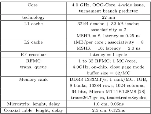
[image:3.612.66.543.52.237.2]L1 core
Figure 1: left: a. traditional memory path; right b. RFiof memory path;
for a 32-core-processor we examine up to 32 RFMCs, or al-ternatively, core:MC ratios from 1:32 to up to 1:1.
Given that RFpins are scalable, we demonstrate architec-tural RFMC scalability and latency benefits, as well as its performance effects in two independent but complementary ways: (a) memory parallelism benefits through the use of RFpins; (b) latency improvements when transferring bursts and memory commands at the speed of light [34], i.e., by re-ducing the wire delays between the RFMC and rank. Having a MC-baseline correspondent to an electrical-based version with I/O pins scaled under ITRS I/O pin constraints, our findings show that employing standard 1333 MT/s DDR3 ranks (Table 2 contains the complete settings) interfaced to appropriated RF TX/RX, RFMC scaling and RF latency benefits improve bandwidth and performance respectively by a factor of 7.2x and 8.6x, when compared to the base-line. Moreover, since bandwidth and (b) latency are directly related, we observe around 69% of latency reduction.
To evaluate RFiof area and power benefits, we employ the methodology proposed in [24], which evaluates the architec-tural benefits of replacing MCs with RFMCs. As a result, we observe a MC area saving benefit of up to 65.6%, which can be alternatively seen as replacing each MC with 2.8 RFMCs, thus allowing larger RFMC scalability and improving band-width. Furthermore, we show that MC I/O pads are elimi-nated in RFiof, which may reduce chip-fabrication costs as a consequence of MC I/O pad area reduction. In terms of power / energy, our findings show that replacing MCs with RFMCs can save up to 80% of interconnection energy. This paper is organized as follows: section 2 discusses the I/O pin problem. Section 3 presents RFiof, compares it to tradi-tional, and to high-scalable pin solutions. Section 4 presents the experiments and results. Section 5 presents the related work, and section 6 concludes it.
2.
THE I/O PIN PROBLEM AND SCALABLE
SOLUTIONS
Through this sequence of experiments, we illustrate how the I/O pin problem limits bandwidth in regards to pin counts. Furthermore, we show why current solutions are not scalable, and what is behind high-bandwidth I/O pin scalable solutions such as RF, optical, and 3Dstacking.
2.1
Background/Motivation: The I/O pin
prob-lem
We start briefly listing the representative background
rea-son elements of the I/O pin problem: (i) electromigration at higher clock rates and pitch size densities; (ii) crosstalk due to likely higher route densities [13]; (iii) giving smaller dimensions, an I/O-pad-to-PCB-pad reliable connection is likely to be challenging. All three aspects affect bandwidth. Before describing the motivations for higher pin / band-width demands, we first define the electrical baseline MC-count, using the scaling predictions of MC/pin counts ver-sus MC-count by Polka [1] and ITRS [13], as well as current 16-core-4MC-AMD Bulldozer processor. We conclude that 32-core OOO processors are likely to have 5 MCs (32:5 core-to-MC ratio), defined as the baseline MC-count.
To investigate the I/O pin problem, we employ the method-ology proposed by Marino [22], not to I/O pads, but to I/O pins, which consists comparing the potential performance of RFiof with RFpins – obtained at 1:1 core:MC ratio, with the baseline under MC I/O pin constraints, in two experiments. (i) the bandwidth of one rank is obtained to proper cali-brate the system; (ii) the first experiment is extended from 32:1 up to 32:32 core:MC ratios (32:32 equivalent to 1:1), by proportionally increasing I/O pin counts with MC counts. Then, bandwidth and MC I/O pin usage of these core:MC ratio ranges are obtained and compared to the baseline ones. Before summarizing the experiments, we point that we have selected a generic DDR3 memory rank employed in PCs, (64 data bits, 1333 Mtransactions/s or MT/s) based on the Micron model MT41K128M8 of 1GB [28], described in table 2. The two experiments were modeled employing M5 [30] and DRAMsim [8] simulators, with the following set-tings: (i) a bandwidth measurement using STREAM mem-ory intensive benchmark [26] (table 3) is experimented for a set formed by one core (1 core, 4.0 GHz 4-wide OOO core, one MC at 4.0GHz), one crossbar with 1-cycle latency – fur-ther described in table 2, and one MC connected to just one rank (to extract its maximum bandwidth); (ii) this set configuration is extended to a 32-core system with core:MC proportions varying from 32:1 to 32:32 (or 1:1).
Figure 2: bandwidth demand for 1:1 core-to-MC ratio for 32 cores and I/O pin counts
are dedicated to control/data/address signals (240 on total). Regarding I/O pin usage, Figure 2 presents the result of experiment (ii) with different core:MC ratios and shows that employing 32 ranks would require 32 * 240 = 7840 pins, which is a significant amount, and if used would require larger package area, routing, and costs.
Additionally, other examples [3][4][6][10][36] of significant pin/MC counts are AMD Bulldozer-4 MCs/2000pins, NVidia GT200 - 8MCs/2495pins, Tilera TILE64 - 4MCs/1500pins, and finally the 192-core Cisco-IBM CRS-1 router - 16 MCs.
2.2
Current memory solutions do not scale
We define the bandwidth per pin as:
bw pin=bandwidth rank/number of IO pins (1)
Typical DDR-family design involves the utilization of wider buses and larger clock frequencies - both as numerator pa-rameters of (1) - to achieve high bandwidth per pin. More-over, using the 180-240 I/O pins/MC range and typical 17GB/s-data-rate reported by Polka [1] as inputs to equa-tion (1), it produces a low-magnitude bandwidth per pin of 2Gbits/s/pin. Intel FBDIMM [12] employs a pair of serial differential short-wide high-speed busses to connect MC and a cache buffer (responsible for a large power con-sumption) placed at the ranks to achieve 48 pins/MC and a 2.5Gbits/s/pin-data-rate, while RAMBUS XDR2 [33] uses a high speed serial signaling with adaptive equalization (by removing the signal resistor-capacitor component over serial transmission) to achieve 32 pins/MC and a 12.8 Gbits/s/pin-data-rate [33]. We observe that these two commercial solu-tions provide larger bandwidth per pin and reduced pin us-age than DDR memories, however their still significant I/O pin-count magnitudes do not allow MC scalability, which triggers the search for high-pin-scalable mechanisms.
2.3
Pin-scalable: Optical and RF
We note that general mechanisms that contribute to high-pin scalability are not only exclusive to optics [7], but also of RF [22]. Researchers report [34] that in RF, signals travel at close-to-light speed, with significant low-magnitude energy utilization for 1mm-30cm distance-range [20][35], and, as in optics, Frequency Division Multiplexing mechanism (FDM – data are carried by different frequency bands) is employed. Finally, to the previously mentioned factors, its lower costs
and CMOS fabrication maturity aspects mentioned in [35] favors RF comparatively to optics.
Since high pscalable solutions use modulation, we in-corporate this mechanism into equation (1):
bw pin=ncarrier∗data rate/number of IO pins, (2)
Using Corona [7] scalable 2-I/O-optical-pins per MC and its wavelengths (carriers), we have:
bw pin= 160GBytes/s/2pins, (3)
or 640 Gbits/s/pin, which is much larger than current solutions such as the 12.8Gbits/s/pin obtained in RAM-BUS XDR2 [33]. Furthermore, Corona [7] employs half of pins used in typical RF solutions (4RFpins, 50Gbits/s/pin ranges), such as RFiof (details in section 4.1) can provide.
2.4
Comparing RF, 3Dstacking, and Optical
We now compare electrical/3Dstacking, optics, and RF under different aspects. In RF and optics, reports [15][21][35] indicate that the typical time range for up-conversion/down-conversion from data to light / RF waves and vice-versa delays is similar in optical and RF – about 200 ps. Fur-thermore, researchers [31][35] observe that optics presents a higher loss if compared to RF, since at this point, in terms of fabrication integration, optical and electrical are not as closer as RF and electrical.
The employed number of optical carriers is distant (4-12/64) from the theoretical limit(256), thus needing to ma-ture if compared to RF. Confronting Frank Chang [21] and Kirman [31] studies, we observe that waveguides width/pitch to minimize crosstalk have a similar behavior in optics and RF. In terms of power and temperature, respectively an ex-tra bus is needed for the optical laser power and optical cir-cuits are reported [21] to be very sensitive, while RF follows CMOS. In terms of transceiver area, we notice that both technologies are reported [15][21][35] to use similar ranges.
We now compare RFiof and 3Dstacking. Regarding laten-cies, since researchers [20][21] indicate that RF-signals take around 100ps to travel 1cm-distance, we estimate that to travel 2.5cm - RFiof RFMC-to-rank distance, signals take around 250ps. However, in 3D-stacks systems, reports [19] indicate that to traverse 200 µm-1000 µm - equivalent to a 20-layer stack, signals take around 12ps, thus having 20x smaller delays when compared to RFiof. Regarding rank width, while typical 3Dstacking has 64-128 Byte-wide ranks, RFiof ranks are 8Byte-width ones, to keep typical rank width-size compatibility. Considering vertical RF-lines - as re-placement of TSVs in 3D-stack systems - were employed to transfer larger width-ranks, they are likely to demand more RFpin related structures (microstrips and microstrip-to-coaxial interfaces), but not RFpads - replacement of I/O pads – since RFpads or equivalent are embedded and not respectively present either in RFiof or in 3Dstacking. In the latter, ranks are placed on a different 3D-layer, and when these and MCs are scaled, processor temperature is reported to be affected [11]. However, since RFiof is configured with typical ranks placed on the motherboard, ranks do not affect the processor temperature and heat dissipation.
3.
RFIOF
[image:4.612.61.288.56.246.2]DRAM rank
control bits
data bits
data bits
...
RFMC
cache line
cache line
request (address)
DRAM banks
control in control out
RX TX
data out
data in RX
TX
line control
coaxial cable
RFpin
line data
coaxial cable
TX
RX
RX TX
data buffer out
data buffer in
transaction processing engine
front end engine
substrate microstrip
trench
outer connector
coaxial cable
to other chip
center connector
substrate
substrate trench
microstrip
flipped microstrip flipped trench
to other chip
chip side face
coaxial cable outer connector coaxial cable
[image:5.612.67.548.55.213.2]to other chip
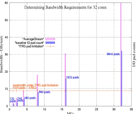
Figure 3: left to right: (a) RFiof memory design; (b) microstrip/trench ; (c) multiple cables interface and side view.
In order to connect processor and memory, RFiof employs the following methodological principles: (i) RF-design, (ii) minimization of components, (iii) low cost, and (iv) CMOS integration, which analysis, modeling and formulation, are discussed in the following sections.
3.1
Overview and Analysis
Regarding (i), the use of elements not designed according to RF-rules is likely to cause undesirable bandwidth degra-dation effects such as reflections, distortions, and dispersion effects at high-frequencies, thus causing signal loss and con-sequently bandwidth reduction. Since traditional I/O-pin-related structures are difficult to be implemented with con-trolled impedances, the previously bandwidth-degradation effects are likely to happen in this frequency-range.
Typical I/O pin structures, as illustrated in Figure 1a, have plenty of elements and are not matched in terms of impedances. (ii). Furthermore, PCB buses are long and significantly capacitive structures [18]. To address these ef-fects in RFiof, impedances between two consecutive elements along the chain of the signal path are matched to avoid signal reflection at high frequencies. The proper impedance match-ing also reduces capacitive effects, which decreases reflection effects, thus minimizing bandwidth degradation. RFiof ele-ments [17] are described along the next subsections.
To contrast with typical memory path elements such as MC and I/O pin elements, RFiof utilizes a RFMC, mi-crostrip, microstrip trench, and a coaxial cable. Figures 1b and 3a respectively illustrate individual RFiof general scheme, its elements and their interconnection.
In RFiof, RFMCs are responsible for memory control, memory data transfers, and modulation of data/commands into RF, while the microstrip and microstrip-trench-to-co-axial interface are functionally similar to MC traces as well as an interface for the coaxial cable. And, the end of the path, we have TXs/RXs at the DRAM rank [17][25][29] which bring the signals from RF domain to digital.
Regarding (iii), RFiof employs a coaxial cable to connect RFMC and each rank, which is simple, modular, and indi-vidually upgradable if connected to faster memories, while cost-effective by reducing motherboard costs via elimination of PCB traces and vias connected to MCs. Moreover, the RF cable presents typical lower cost than a fiber.
About (iv), elements such as microstrips and interfaces -such as microstrip-to-trench interface, are very commonly employed in RF. Furthermore, these elements are tradition-ally fabricated in CMOS, which allows a better integration with traditional digital, when compared to optical elements.
By construction, a microstrip is designed with impedance and propagation constant as a function of the dimensions and dielectric material so that multiple carriers can be si-multaneously transmitted while keeping low delays [29]. Its propagation delay is a function of the dimensions and the dielectric material as further described in section 3.5.
Figure 3b illustrates several interface elements. The micro-strip-to-coaxial interface allows the RF signals to be trans-ferred from the microstrip to the coaxial cable - selected as media as explained in the next paragraph. It is imple-mented according to the previously mentioned RF-design methodology, thus allowing dispersion control [17]. Accord-ing to Lameres et al. [17][16], the microstrip trench is etched into the die substrate and then plated with conducted mate-rial, while the polygonal shaped trench guarantees mechani-cal alignment and supports the microstrip-to-coaxial trench [16]; both techniques and the Lameres [16] fabricated proto-type demonstrate RFiof potential fabrication viability.
The coaxial cable - adopted due to its mobility, flexibil-ity, upgradabilflexibil-ity, and low cost - connects the trench at the RFMC to ranks placed around the cores. Coaxial cables can be fabricated with very small diameters. For example, a 3mm-diameter, 400-GHz range one, is fabricated by Micro-coax [27], and is appropriate for RFiof use.
3.2
RFiof signal path
Before showing RFiof signal path, we show that a typi-cal MC signal path for purposes of reference. As shown in Figure 1a, at the flip-chip package interface, the signal path generated in the MC goes through the following path: MC, package trace, package via, repeaters, the structures which form the I/O pins – such as I/O pad, solder balls, and PCB pad–, and finally the signal reaches the PCB trace, and PCB via, followed by the same sequence in the opposite order when these signals traverse back from the rank to the MC.
In RFiof, TX/RX are placed at RFMCs and ranks (which were presumed as single chips). The path of the signals upon a cache request (Figure 1b) is as follows: at the RFMC TX, the digital address is are converted to analog waves and, after they traverse the microstrip, they are sent through the microstrip/microstrip-to-coaxial interface, coaxial cable, and reach the rank RX – where the analog waves are con-verted back to digital, finally reaching the rank. The signal does traverse the same path in the opposite direction when a rank responds with the data burst. At the RFMC RX, it is converted down back and achieves the processor.
3.3
Ranks
sin-gle chips (Figure 1b), so that the microstrip can be used to exchange requests and responses signals via TXs and RXs. The microstrip total length and cable length are kept at minimum to guarantee minimum delays and lower costs.
3.4
Extension: Proposal to Fit Many RFpins
We propose an extension of Lameres design [17][16], orig-inally designed to work with frequencies up to 60 GHz, con-sidering that these elements follow RF-modeling proposed by Frank Chang et al. [21][25], described in more details in section 3.5. These models presuppose elements designed for RF-frequency ranges, and have their fundamentals on the extensive RF-design and validation techniques, while very commonly utilized in the RF-area [21][25][34]. Furthermore, these models were vastly employed for different purposes (caches, memory) and at different ranges of frequencies [20] [21][39], the latter which we envision in the proposed ex-tension, after re-designed to operate at a larger frequency range, aiming to scale RFpins. RFiof employs microstrips which belong to the class of elements employed in these mod-els. Regarding the used cable (table 2), it is designed to work properly at the targeted frequency, with appropriated construction parameter [27].
The proposed extension aims to scale RFpins, addressing the following restrictions: (i) typical coaxial cable dimen-sions are significant large when compared to typical package dimensions; (ii) each RFpin connects an RFMC to a rank. Before we describe the proposed extension, we point out that we presume typical package dimensions of 20mm x 20mm, and that since 3mm-cables coaxial cables are fabricated [27], thinner-diameter cables can be fabricated.
The extensions proposed are restricted to the microstrip and MEM-trench infrastructure. Starting from the set formed by the microstrip and micro-strip-to-trench structures showed in Figure 3b, we superpose another similar set, but flipped -illustrated on the left of Figure 3c. The 8 cables are arranged in rows, side by side, so that they can be fit in one package side (20mm - right of the Figure 3c), allowing 32 coax cables, which connect the 32 RFMCs to the (32) respective ranks.
3.5
Delay Modeling and Formulation
We start this subsection briefly describing about RFiof circuitry and its modeling. We further explain how the cir-cuitry and modeling incorporate reduction of transmission errors and noise margin. We also explain what are the es-sentials of the modeled RF circuitry and how the models behave with technology improvement.
Generically regarding RF circuits, researchers [34] report that RF signals are mostly represented by its LC (inductive-capacitive) part, and that inductors [21] – dominant in TX / RX circuits – are inversely proportional in size to the op-erational frequency. Thus, according to ITRS [21], due to frequency scaling and consequent carrier frequency scaling, TX/RX area also scales down. Similarly, according to [21], the number of channels available is also expected to scale due to the availability of faster transistors.
As previously mentioned and justified in section 3.4, we as-sume RF-circuitry modeling and scaling proposed by Frank Chang et al. [21][25] are valid for RFiof, which is also the same methodology adopted by other reports [21][20][35]. In these models, modulation and line separation are taken into account in order to keep a low bit error rate (BER). Further-more, according to these models, maximum data rate and number of available channels scales with technology (rule of thumb: maximum data rate as half of the maximum carrier). In addition, these models also take noise margin reduction and differential transmission into account – via doubling the
technology (nm) 45 32 22
carriers 10 12 14
data rate per 7 8 10
band (Gbits/s)
total data rate 70 96 146
per wire (Gbits/s)
space between 28 32 36
carriers (GHz)
power (mW) 60 72 84
energy per 0.85 0.75 0.6
bit (pJ/bit)
area (TX + RX) 0.0115 0.0119 0.0123
(mm2)
area / (data rate) 164 124 88
[image:6.612.344.525.50.208.2](um2)/Gbits/s
Table 1: replicated results from modeling RF technology obtained from [13][21]
number of lines to minimize crosstalk effects as further de-scribed in section 4.1.
Moreover, this modeling also envisions that dispersion and distortion levels of RFiof structures are tolerated accord-ingly. The models incorporated in this methodology were validated and prototyped, as well as they are valid for trans-mission lines such as microstrips employed in RFiof, and follow ITRS [13][21][35]. Typical parameters provided by these models are data rates per carrier, space between car-riers, total data rate per wire, as well as area and power of the TX/RX RF circuits, as illustrated in Table 1.
We change to the delays estimation in RFiof. The overall delay of RFiof is given by the summation of the delays over the microstrip, trench, the coaxial cable, and the other side of the microstrip again, but on the other chip. To calculate the microstrip delay, we use the equation derived from [29]:
Tµpd= 1.016 p
(0.475∗ǫr+ 0.67)ns/f oot (4) whereTmupd is the microstrip delay andǫr is the dielectric coefficient of the microstrip. Regarding the coaxial propa-gation delay, the following equation [29] is valid:
Tcoaxialpd= 1.016 p
(ǫr)ns/f oot (5) whereTcoaxialpd is the coaxial delay andǫr is the dielectric coefficient of the coaxial cable. The rest of the delays is discussed in the following section.
4.
EXPERIMENTAL SECTION
In this section, we determine RFpin counts scaling for different memory technologies and types, using a similar methodology to the proposed by Marino [23], but applied to I/O pins. Furthermore, we compare RFpin count with other technologies such as optics, electrical, and 3D-stacking. In the sequence, we employ the methodology proposed in [24] to estimate area and power architectural benefits of replac-ing MCs with RFMCs in RFiof. After that, we discuss the methodology and bandwidth/speedups results obtained when scaling RFMCs, as well as observe latency reduction via transaction queue occupancy and duration reduction.
4.1
RFpin count / dimensions: matching
cur-rent ranks and future memory scaling
Gbits/s-data-0 2 4 6 8 10 12 14 16
1000 2000 3000 4000 5000 6000 7000
Number of RFpins
Memory frequency
RFpins x Memory Scaling
design@22nm_200GHz design@22nm_400GHz
design@16nm_200GHz design@16nm_400GHz
0 0.5 1 1.5 2 2.5 3 3.5 4
45nm 32nm 22nm
Area (mm2)
technology (nm)
Area: MC x RFMC for different technologies MC
RFMC MC
RFMC MC
RFMC FE
TE
PHY RF TX/RX
0 0.5 1 1.5 2 2.5
45nm 32nm 22nm
Power (W)
technology (nm)
MC/RFMC FE and TE power for different technologies
[image:7.612.40.289.54.383.2]FE TE
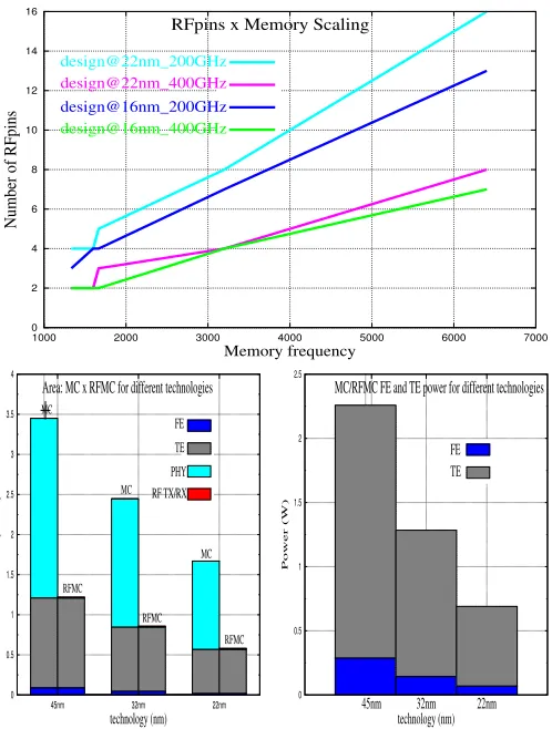
Figure 4: top to bottom, left to right: (a) RFpins versus memory scaling; FE/TE (b) area and (c) power
rate per carrier. Given the coaxial cable maximum upper limit frequency (400GHz), half of that is available to the carriers (Nyquest): thus 5 carriers, each with 10 Gbits/s-data-rate, provide an RFMC data rate budget of 50 Gbits/s. To illustrate the design of the RF interface, we particu-larly chose a DDR3 memory due to its large employment in general PCs and due to its significant pin counts (180 - 240). Once the delays through TX/RX are very small – within 200-picoseconds range [21] – when compared to the memory timing operations, they are not considered in the following formulations. The module particularly chosen is the Micron MT41K128M8 of 1GB (64 data bits, 1333 MT/s, table 2), with significant pin counts (180 - 240), and experimented in section 2.1. To determine RFpin counts we define:
RF pins=number of I/O pins per RF M C (6)
and the memory throughput is defined as:
m throughput=m cycle∗tot bits transf erred, (7)
where m cycle is the memory cycle. Using m bits as the amount of memory bits transferred in one memory cycle, we have in the sequence :
RF pins f or data=f loor(data m bits/m throughput) (8)
Then, using modulation and high-speed signaling to transfer memory bits in equation (2), we have:
m throughput=m cycle∗RF data rate∗ncarrier (9)
And, for data bits (data - d), we then have:
RF pins d=f loor(d m bits/d m throughput) (10)
where data refer to data bits, such as a burst. Similarly, for control bits (control - c):
RF pins c=f loor(c m bits/c m throughput) (11)
And finally,
RF pins=RF pins d+RF pins c (12)
To determine the number of RFpins needed, we determine the total amount of data bits transferred in one memory cycle, which we define as tot bits:
tot bits=total amount of bits in m cycle (13)
We now exemplify RFpin count calculation for the target rank. Inspecting the rank and similar ones in Micron DDR3 catalogs [28], except voltage, ground, and not-connected pins, the total number of pins effectively used for data trans-mission in a rank access - composed by a sequence of oper-ations on the control and data busses - is around 123 bits (around 50%, with 64 for data, 59 for control of a total of 240 pins). Examining rank pin usage and timing, equation (13) shows that in one memory cycle we can have:
tot bits= (1/1333M T /s)∗5carriers∗10Gbits/s, or (14) tot bits= 37.5bits;f loor(37.5) = 37bits, (15) i.e., 37 bits can be transferred in one memory clock period, along one RFpin. Hence, 2 RFpins are necessary to carry all the 64 data bits and 2 RFpins for the 59 control bits needed, for a total of 4 RFpins. This RFpin count is scalable and has a similar magnitude to Corona 2-optical pin-count showed by Vantrease et. al [7]. Figure 4a shows the result of RF scaling (combination of equations 3 to 10) with memory frequency scaling at 16nm; from this figure, we observe low-magnitude RFpin counts for different memory generations, even for memories with larger clock frequencies than DDR4 ones. In addition, disregarding the 400GHz-upper-limit, we observe RFpin-scalability equivalent to 2-optical pins.
Compared to traditional memory solutions, RFiof respec-tively presents a pin reduction of 16x and 24x if compared to RAMBUS XDR2 and Intel FBDIMM. Compared to optical-pins, RFiof has 2x more I/O pins (4 RFpins) or the same count if the 400GHz upper limit is disregarded.
Analyzing ITRS predictions [13], we have found that around 512 (rounded) pins are exclusively dedicated to memory, once there are pins related to other elements (for exam-ple, PCI). Assuming a typical DDR3 240-pin budget and the area estimation (50%), we can potentially save up to 46.9% ((123+123)/512) of the die area dedicated to the I/O pins. Considering applying this RFiof technique to cur-rent 2-4MC-microprocessors, potentially up to 492 I/O pins, which correspond to 4.920000 mm2 of area saving can be obtained, with the typical 1000 um2 per pin [13]. Further-more, assuming similar pad-to-pin rates, similar area pad reduction could be obtained. Moreover, this analysis over-estimates the number of control signals simultaneously used (clock included), which optimization is not presented due to space reasons. Finally, the investigation of having both con-trol / data lines buffered and sequential transmission over a unique microstrip line are left as a future investigation.
4.2
Area and Power Analyses
1 1.5
0 0.5 1 1.5 2 2.5 3 3.5 4
Energy per bit (pJ/bit))
distance (cm)
RF energy versus distance
energy versus distance
0 50 100 150 200 250 300 350 400 450
0 5 10 15 20 25 30 35
pChase Latency (ns) and Energy per bit (pJ/bit)
Number of MCs
pChase: measured latency (ns) and Total Rank Energy per bit
baseline latency: 5 MCs
latency_RFPM
baseline latency: 5 MCs latency_RFPM_burst_commands
[image:8.612.58.290.54.343.2]total_energy_rank_per_bit
Figure 5: left to right: (a) energy versus distance replicated from [35]; (b) RFiof total rank energy and pChase latency
strategy employs RF RX/TX area dimensions obtained via Frank Chang et al. circuitry modeling estimations [21][35], such as the ones listed in Table 1.
4.2.1
RFMC versus MC area (baseline)
The proposed methodology is applied to the (i) MC versus RFMC area comparative aspects. As a result, we observe in Figure 4b that for different technologies, the area of one RFMC corresponds to around 36.5% of the area of one MC, i.e., considering the MC area as area budget, we can fit up to 2.8x more RFMCs on the die, which means that, for the multicore baseline (5 MCs - section 2.1) MC-area, we can have up to 14 RFMCs within this same area budget.
4.2.2
RFiop TX/RX Rank area
To estimate area dimension of the TX/RX area at the rank, we employ a similar methodology to the one used in previous subsection. While the results of this estimation indicate an area of about 0.015-0.0123 mm2 - a small area overhead, considering typical fabricated memory die area of 50 mm2 [28]. To further broaden this estimation, given the RF-memory prototype reported by Byun et al. [9], which has TX/RX area of about 0.094 mm2, the overhead of this area compared to the total chip area is still not significant.
4.2.3
MC versus RFMC power comparison
We organize the following analyses to identify RF power and energy benefits of RFiop and comparatively analyse it to the respective MC counterpart in each part of the memory path: (1) MC power comparison; (2) RFiof interconnection energy; and (3) rank power and total rank energy.
As previously mentioned in section 4.2.1, we adopt Marino’s methodology [24] to compare FE/TE power in MC versus RFMC, since both are either present in RFMC and MC (obtained via McPAT tool [37]). These magnitudes are il-lustrated in Figure 4c, where we observe that for different
technologies (45, 32, and 22nm), FE/TE power decrease as technology improves - justified by the improvement of tech-nology as the transistors size shrink as mentioned in [37].
Concentrating on the MC PHY power, most represented by the amount of bits transferred, it is the most power rele-vant when compared to the FE and TE, We envisioned this as a component of the dynamic energy, which includes I/O pin power, and is analyzed in the following section.
4.2.4
RFiof interconnection energy
To perform the interconnection energy determination, we employ the power versus distance projection from Tam et al [35] which is replicated in Figure 5a, and apply it for the average distance between RFMCs-ranks, estimated as 2.5 cm. As a result, we obtain 1.2 pJ/bit for the interconnec-tion energy. To determine the MC interconnecinterconnec-tion energy, we measure the PHY power provided by McPAT [37] and divide by the amount of transferred bits, in a similar ex-periment as the one performed in section 2.1; we obtained around 6 pJ/bit. Thus, we estimate that the interconnec-tion energy savings are about 80%. With a similar strategy as the one utilized when performing RFMC area comparison (section 4.2.1), we estimate that we can fit up to 25x more RFMCs, which alternatively represents an architectural ben-efit. Since the area benefits obtained in the section 4.2.1 are smaller (equivalent to 14 RFMCs), we conservatively assume the latter as the dominant and do not determine the archi-tectural performance benefits related to power.
4.2.5
Rank Power and Total Rank Energy
Since TX/RX elements are part of RFiof transmission, RFpin power is consumed as a replacement of I/O pin ter-mination power. Using a similar approach as the one used to compare RFMC versus MC power, combined to Micron DRAM sheet power, we determine the rank power. As a re-sult, we can save up to 6.7% of the DRAM power in RFiof. In order to determine the total rank energy usage, we performed the following calculation:
memory energy=total power / total bandwidth (16) To obtain the rank power, we employ Micron data sheet parameters [28] combined to DRAMsim [8], which provides the total number of memory accesses. Total rank energy contemplates the total dynamic and static energy of the set formed by all employed ranks. Bandwidth measurement was obtained via experiment with similar settings as performed in section 2.2, with different RFMC/MC counts. The re-sults of this experimentation are shown in Figure 5b, which demonstrates that memory energy usage decreases in up to 43.9% compared to the baseline (baseline reference with 5 MCs, as explained in section 2.1) as we increase MC counts, given that the high memory bandwidth scaling obtained via RFMC scaling is proportionally higher than power scaling (equation 16). An important observation is that although energy levels usage showed are significantly high, i.e. up to 240 mW/bit, these magnitudes are at these levels due to the DDR3-rank model selected. Since RFiop is compatible with DDR-memory family, it could certainly be applied to low power ranks, such as LPDDR2 ones.
4.3
Methodology, Bandwidth, and Speedups
Before describing the methodology, we observe that we do not include optical modeling due to to the fact that, for the distance traversed, typical optical delays do have similar magnitudes to RF [15][21][35], which would result in similar bandwidth / speedups / latency behavior (adopting the same settings for other hardware elements).
Core 4.0 GHz, OOO-Core, 4-wide issue, turnament branch predictor
technology 22 nm
L1 cache 32kB dcache + 32 kB icache;
associativity = 2 MSHR = 8, latency = 0.25 ns
L2 cache 1MB/per core ; associativity = 8
MSHR = 16; latency = 2.0 ns
RF crossbar latency = 1 cycle
RFMC 1 to 32 RFMC; 1 MC/core,
trans. queue 4.0GHz, on-chip, close page mode
buffer size = 32/MC
Memory rank DDR3 1333MT/s, 1 rank/MC, 1GB,
8 banks, 16384 rows, 1024 columns, 64 bits, Micron MT41K128M8 [28] tras=26.7cycles, tcas=trcd=8cycles
Microstrip: lenght, delay 1.0 cm, 0.06ns
[image:9.612.53.300.51.238.2]Coaxial cable: lenght, delay 2.5 cm, 0.125ns
Table 2: modeled architecture parameters
[8] simulators . Memory transactions are generated by M5 and captured by multiple MCs/RFMCs in DRAMsim, which respond with the result of the memory transaction.
To evaluate RFMC scalability, we observe that our exper-imentation covers different core:MC ratio (1:1/32, 1:1/16, until 1:1), or put differently, with different RFMC counts (1 to 32) for 32 cores. In addition, we restate that the baseline has 5 MCs (discussed in section 2.1). In order to evaluate MC scalability, we have employed the most conservative ad-dressing mode by interleaving cache lines along the RFMCs, so that we do not take advantage of locality. Moreover, in order not to take advantage of locality benefits, we have em-ployed closed page mode (server environment) in all of the experiments [8]. The memory timing parameters are based on rank previously analyzed (section 2.1, 1GB DDR3, Mi-cron model MT41K128M8 [28]).
To guarantee enough pressure on the memory system, we have utilized an OOO processor model. The processor mod-eled follows a clustered architecture, where we have one core per L2 slice, i.e., private L2 slices in order to avoid cache sharing effects. The ISA employed is based on Alpha proces-sor, configured as a 4-way issue OOO core as typical current processors [3]. Furthermore, we presumed a banked and scalable L2 MSHR structure [40]. We assumed 1MB/core as an L2 cache slice size to reflect current OOO processors. L2 slices communicate through an 1-cycle RF-crossbar con-figured with same latency assumption of Frank Chang [21] study: 200ps of TX-RX delay, plus the rest of the cycle to transfer 64 Bytes using high speed and modulation. We ob-tained cache latencies from Cacti [5] and adopted MSHR counts for each L2 slice similarly to the 3D-stack study by Loh [18] reflecting configuration of a real processor.
Regarding memory delays, we have utilized typical two cycles for command-duration period and eight cycles for a burst-duration; due to the speed-of-light property of RF, we estimate that the command-duration delays are reduced from two to one cycle and the bursts, from eight to one cycle. PCB delays are not included in the baseline modeling since we found a broad variety of magnitudes; due to that, the baseline measurements, such as bandwidth / speedups, are closer to the ideal case, i.e., RFiof-likely bandwidth results are better than ones achieved here.
We estimate the coaxial-cable length size of 2.5cm and total microstrip length size (both microprocessor and rank) around 1.0 cm, with microstrip / coaxial cable delays re-spectively using equations (4) and (5), section 3.5. As a
Benchmark Input Size read:write, MPKI
Copy, Add, Scale, Triad 4Mdoubles per 2.54:1 , 54.3
(STREAM) core, 2 iterations
pChase 64MB/thread, 158:1 , 116.7
3 iterations, random
Hotspot (Rodinia) 6000 x 6000, 3 iter. 2.5:1 , 12.5
CG: Conjugate Class A 76:1 , 16.9
Gradient (NPB) 3 iterations
MG:Multigrid (NPB) Class A, 3 iterations 76:1 , 16.9
SP: Scalar Pentad (NPB) Class A, 2 iter. 1.9:1 , 11.1
[image:9.612.315.579.51.177.2]FT: Fourier Trans. (NPB) Class A, 3 iterations 1.3:1 , 6.8
Table 3: benchmarks and input sizes
result, we obtain about 0.06ns and 0.125ns in terms of de-lays using the typical dielectric constant magnitudes of 4.5 and 2.1 from [17], respectively for the microstrip and coax-ial cable. These delays were incorporated into the modeled interconnection in M5. To finalize, table 2 summarizes all parameters we employed in the simulation environment.
Using Loh’s criteria [18], we selected memory bandwidth-bound benchmarks, focusing on the ones with a significant number of misses per kiloinstructions (MPKI) to stress the memory system. Above the selected benchmarks, we have (i) STREAM [26] suite, which we decompose in its four sub-benchmarks (Copy, Add, Scale, and Triad); (ii) PChase [32] with pointer chase sequences randomly accessed; (iii) Hotspot from Rodinia suite [38]; (iv) Conjugate Gradient (CG), Scalar Pentadiagonal (SP), Multigrid (MG), and Fourier Transform (FT), these all from NPB [2]. STREAM and pChase are designed to evaluate bandwidth, while the lat-ter also evaluates latency. The selected NPB applications reflect the bandwidth aspect of the HPC challenge [2].
Table 3 summarizes the benchmarks experimented, input sizes, read-to-write rate, and L2 MPKI obtained in the ex-periments. In all benchmarks, the parallel regions of inter-est were executed until completion. All the input sizes are larger than the total memory size, which guarantees that all the memory space is stressed. The average results were calculated based on harmonic average.
4.3.1
Bandwidth, Speedups, and Related
We define the following terminology:
• baseline: MC scalability under I/O pin constraints. The baseline has 5 MCs, and 32 cores, according to the methodology employed in section 2.1.
• RFiof: defined as the proposed version, i.e., evaluating the RFMC scalability.
• RFiof burst command: difference between RFiof plus RF latency benefits, and RFiof.
• RFiofa: defined as the RFiof version with the same area budget as the baseline to explore its architectural benefits in terms of higher RFMC counts (RFMC area saving). It is obtained by RFiof extrapolation and has 14 RFMCs (discussed in section 4.1).
0 1 2 3 4 5 6 7 8
1 2 4 8 14 16 32 1 2 4 8 14 16 32 1 2 4 8 14 16 32 1 2 4 8 14 16 32 1 2 4 8 14 16 32 1 2 4 8 14 16 32 1 2 4 8 14 16 32
Bandwidth, Occupancy, Duration: normalized to the baseline (x times)
number of MCs
Bandwidth, Transaction Queue Occupancy - - Average Duration - 32 cores
RFiof RFiof_burst_command RFiofa (14 RFMCs) RFiofa_burst_command (14 RFMCs) "baseline (5 MCs)" Add
Copy
Scale Triad
pChase
Occupancy
Duration
0 1 2 3 4 5 6 7 8 9
1 2 4 8 14 16 32 1 2 4 8 14 16 32 1 2 4 8 14 16 32 1 2 4 8 14 16 32 1 2 4 8 14 16 32 1 2 4 8 14 16 32 1 2 4 8 14 16 32 1 2 4 8 14 16 32 1 2 4 8 14 16 32 1 2 4 8 14 16 32
Speedup normalized to the baseline (x times)
number of MCs
Speedup Normalized to the baseline - 32 cores
RFiof RFiof_burst_command RFiofa (14 RFMCs) RFiofa_burst_command (14 RFMCs) "baseline (5 MCs)" Add
Copy
Scale Triad
pChase
Hotspot
[image:10.612.47.543.30.345.2]CG FT SP MG
Figure 6: left (a) bandwidth, transaction queue occupation and duration; right: (b) speedups; RFiof: RFMC scalability; RFiofa: RFiof under area budget; RFiof burst command/RFiofa burst command: RFiof and RFiofa plus RF latency benefits.
We only show the transaction queue average occupancy and the duration for the most memory intensive benchmarks - STREAM and pChase. The larger RFMC-count allows to increase the number of memory transactions simultaneously served, while transactions queues become shallower and less occupied (on the right of Figure 6a). Compared to the base-line, transaction queue occupancy is respectively reduced of about 86% and 68% for RFiof and RFiofa. Furthermore, the larger RFMC-counts affect the duration of one transaction: as showed in Figure 6a , the average duration is decreased by up to 60% and 40%x for RFiof and RFiofa, with the baseline as reference; alternatively, as the RFMC-counts in-crease, the memory system overall latency decreases, which also confirms bandwidth scaling. Figure 4e shows the aver-age pChase memory latency RFiof; compared to the base-line, this latency is reduced by around 69% through RFMC scalability and up to 69.5% when the high-speed transmis-sion benefits are included.
Figure 6b illustrates speedups obtained across the bench-marks for different core:MC ratio (32:1, 32:2, until 32:32), i.e., different RFMC counts. For all benchmarks, we observe that speedups increase in the same proportion as a result of the larger RFMC availability. For STREAM, RFiof and RFiofa are respectively up to 8.6x and 5.6x faster than the baseline. Similar scaling trends are obtained for pChase, Hotspot, CG, and FT; for these benchmarks, RFiof respec-tively achieved up to 3.23x faster for pChase, 5.0 x for Hotspot, 3.01x faster for CG, 2.63x for FFT, 3.64x for SP, and finally 3.64x for MG, when compared to the baseline version. Accordingly, RFiofa followed a similar improvement trend. The largest bandwidth/speedup improvements occur for the STREAM suite due to its access pattern (stream) and large MPKI magnitudes (Table 3).
We now concentrate on the high-speed RF latency
ben-efits. Regarding commands duration and burst we observe bandwidth improvements of up 25%. Similarly, speedups are improved, for all the selected applications; in this case, speedups are improved by up to 20.4% as illustrated in Fig-ure 6b. In this case, the transaction average duration and occupancy (in this case accounted by decreasing the yellow bar from the total) observed on the right of Figure 6a, are reduced by up to around 67% and 20%. The same trend is also valid for RFiofa, in terms of bandwidth (20%) and speedup (18%). In terms of RF latency decrease, pChase indicates a maximum reduction of about 7.5% (Figure 4e). Moreover, for all the benchmarks evaluated, as the number of RFMCs grows, the RFMC scalability benefits (RFiof) are more dominant than the latency ones (burst command ver-sions), because the transaction queue contention reduction is larger than the latency reduction.
We observe that some benchmarks exhibit traffic imbal-ance between memory controllers in interleaved mode and a speedup saturation for higher RFMC counts. After deeply investigating the simulation infrastructure statistics, we no-tice that some L2 slices presented significantly different miss rates as RFMC-count is scaled; this context presents many similarities to the churn phenomenon described by Loh [18] when scaling MSHRs, which we leave as further investiga-tion. Furthermore, larger input sizes could potentially ad-dress SP and MG speedups saturation after 8/16 RFMCs, since we restrict M5 address space size to 2GB.
5.
RELATED WORK
pads (4 RFpins), disregarding the 400GHz upper limit. The reconfigurable CDMA RF memory bus by Kim et al [14] targets I/O pin-count reduction and bandwidth. How-ever, this solution was not interfaced to MCs, neither to sup-ply the multicore-era bandwidth demands. Moreover, RFiof adopts FDM, reported [25] to present higher bandwidth than CDM used in this CDMA bus. Given this CDMA bus [14], the RF-overlaid with mesh in [20][21], and Tam’s [35] RF-in-future microprocessor design, RFiof employs an equivalent approach regarding RF theory/circuitry modeling.
The DIMM Tree architecture [39] targets off-chip mem-ory, investigating the trade-offs between a multi-drop rank latency versus the RF single-drop latency, as well as the RF bandwidth supplied to each rank versus the number of ranks. While sharing RF, RFiof provides a significantly lesser pin count (around 4RFpins) than DIMM Tree (39 pins). More-over, DIMM Tree focuses on rank scalability using the same RFMC, while RFiof on RFMC scalability.
Marino [24] proposed an on-package RF-memory organi-zation targeting MC-power reduction. While both employ RF, RFiof focuses on I/O pin scalability to explore RFMC scalability, aiming bandwidth and performance. As a follow up paper, Marino [22] extended this architecture to focus on I/O pad scalability; to contrast with the later, which fo-cuses on package-pad reduction, RFiof focus also in I/O pin reduction, which allows larger RFMC scalability.
6.
CONCLUSION AND FUTURE PLANS
We have proposed RFiof memory organization as an ap-proach to the I/O pin problem. In RFiof, MC and typical I/O pins are replaced by RF-designed apparatus, which in-clude RFMCs, RFpins, RF TX/RX, microstrip/-to-coaxial interface, and a coaxial cable. RFiof advantages are many-fold: (i) by removing the MC I/O pin constraints via a able RFpin-count, we demonstrate high bandwidth by scal-ing RFMCs, thus improvscal-ing performance, (ii) die area and (iii) power/energy reduction, (iv) DDR-family compatible, (iv) and a cost-design alternative to optical systems.
As future research points, we plan to evaluate RF ben-efits when communicating to 3D-stack memories, as verti-cal RF-TSVs viability improve. Although RFiof is DDR-compatible, we plan to develop a dedicated rank, to further explore its performance and power benefits.
7.
REFERENCES
[1] Moore’s Law, 40 years and Counting. Accessed date: 09/10/2011 ; http://download.intel.com/technology/silicon/ Interpack.
[2] NAS Parallel Benchmarks. Accessed date: 11/11/2012 ; http://www.nas.nasa.gov/Resources/Software/npb.html/. [3] AMD Reveals Details About Bulldozer Microprocessors, 2011.
accessed date: 11/10/2012
-http://www.xbitlabs.com/news/cpu/display/20100824154814 AMD Unveils Details About Bulldozer Microprocessors.html. [4] The Era of Tera: Intel Reveals more about 80-core CPU.
Accessed date: 08/27/2011 ;
http://www.anandtech.com/cpuchipsets/showdoc.aspx?i=2925. [5] CACTI 5.1. Accessed Date: 10/20/2012;
http://www.hpl.hp.com/techreports/2008/HPL200820.html. [6] The Push of Network Processing to the Top of the Pyramid.
Accessed date: 07/21/2012 ;
http://www.cesr.ncsu.edu/ancs/slides/eathertonKeynote.pdf. [7] Dana Vantrease et al. Corona: System Implications of
Emerging Nanophotonic Technology. InISCA ’08, pages
153–164, Washington, DC, USA, 2008. IEEE Computer Society. [8] David Wang et al. DRAMsim: a memory system simulator.
SIGARCH Comput. Archit. News, 33(4):100–107, 2005. [9] G. Byun et al. An 8.4Gb/s 2.5pJ/b Mobile Memory I/O
Interface Using Bi-directional and Simultaneous Dual (Base+RF)-Band Signaling. IEEE, 2011.
[10] GT 200. Accessed date: 08/27/2012 ; http://www.hardwaresecrets.com/.
[11] Healy, M et al. A Study of Stacking Limit and Scaling in 3D
ICs: An Interconnect Perspective. InElectronic Components
and Technology Conference, pages 1213–1220, Washington, DC, USA, 2009. IEEE Computer Society.
[12] Intel Fully Buffered DIMM. Accessed date: 08/26/2012 – http://www.intel.com/.../FBDIMM/.../Intel FBD
Spec Addendum rev p9.pdf.
[13] ITRS HOME. Accessed date: 09/12/2012 ; http://www.itrs.net/.
[14] Kim, J. et al. Reconfigurable Memory Bus Systems using
Multi-Gbps/pin CDMA I/O Transceivers. InISCAS, volume 2,
pages 33–36, Bangkok, Thailand, 2003. IEEE.
[15] Kobrinsky M. J. et al. On-Chip Optical Interconnects.Intel
Technology Journal, 8(2):129–142, 2004.
[16] LaMeres B. J. et al. Novel 3-D Coaxial Interconnect System for
Use in System-in-Package Applications.IEEE Transactions on
Advanced Packaging, 33(1):37–47, 2010.
[17] LaMeres B.J., McIntosh C. Off-Chip Coaxial to Microstrip
Transition Using MEMs Trench.3D/SiP Advanced Packaging
Symposium, 33(1), 2008.
[18] Loh, Gabriel H. 3D-Stacked Memory Architectures for
Multi-core Processors. InISCA’08, pages 453–464, Washington,
DC, USA, 2008. IEEE Computer Society.
[19] G. L. e. a. Loi. A thermally-aware performance analysis of vertically integrated (3-D) processor-memory hierarchy. In Proceedings of the 43rd annual Design Automation
Conference, pages 991–996, New York, NY, USA, 2006. ACM. [20] M-C. Frank Chang et al. Power reduction of CMP
communication networks via RF-interconnects. InMICRO’08,
pages 376–387, Washington, DC, USA, 2008. IEEE. [21] M. Frank Chang et al. CMP Network-on-Chip Overlaid With
Multi-Band RF-interconnect. InHPCA, pages 191–202, 2008.
[22] Marino, M. D. On-Package Scalability of RF and Inductive
Memory Controllers. InEuromicro DSD. IEEE, 2012.
[23] Marino, M. D. RFiop: RF-Memory Path To Address On-package I/O Pad And Memory Controller Scalability. In ICCD, 2012, Montreal, Quebec, Canada. IEEE, 2012. [24] Marino. M.D. and Skadron K. Reducing Power and Area by
Interconnecting Memory Controllers to Memory Ranks with RF
Coplanar Waveguides on the Same Package. InWEED
Workshop, in conjunction with ISCA, 2011.
[25] Mau-Chung Frank Chang et al. Advanced RF/Baseband Interconnect Schemes for Inter- and Intra-ULSI Communications. 52:1271–1285, Jul 2005.
[26] McCalpin, John D. Memory Bandwidth and Machine Balance
in Current High Performance Computers.IEEE TCCA
Newsletter, pages 19–25, Dec. 1995.
[27] Leading the way in transmission line solutions. Accessed date: 08/13/2011 ; http://www.micro-coax.com/.
[28] Micron manufactures DRAM components and modules and NAND Flash. Accessed date: 12/28/2012 ;
http://www.micron.com/.
[29] A practical resource covering the fundamental principles of microwave design. Accessed date: 10/30/2012
-http://www.microwaves101.com/.
[30] Nathan L. Binkert et al. The M5 Simulator: Modeling
Networked Systems.IEEE Micro, 26(4):52–60, 2006.
[31] Nevin Kirman et al. Leveraging Optical Technology in Future
Bus-based Chip Multiprocessors. InMICRO’06, pages 492–503,
Washington, DC, USA, 2006. IEEE Computer Society. [32] The pChase Memory Benchmark Page. Accessed date:
05/22/2011 ; http://pchase.org/. [33] Rambus. Accessed date: 11/14/2012 ;
http://www.rambus.com/.
[34] Richard T Chang et al. Near Speed-of-Light Signaling Over
On-Chip Electrical Interconnects.Journal of Solid-State
Circuits, 38(5):834–838, 2003.
[35] Sai-Wang Tam et al. RF-Interconnect for Future Network-on-Chip. pages 255–280, 2011.
[36] Shane Bell et al. TILE64TM Processor: A 64-Core SoC with Mesh Interconnect. pages 88–90. IEEE, 2008.
[37] Sheng Li et al. McPAT: an integrated power, area, and timing modeling framework for multicore and manycore architectures. InMICRO’09, pages 469–480, New York, USA, 2009. ACM. [38] Shuai Che et al . Rodinia: A benchmark suite for heterogeneous
computing. InIISWC, pages 44–54. IEEE, 2009.
[39] K. e. a. Therdsteerasukdi. The dimm tree architecture: A high
bandwidth and scalable memory system. InICCD, pages
388–395. IEEE, 2011.
[40] Tuck, James et al. Scalable Cache Miss Handling for High
Memory-Level Parallelism. InMICRO’06, pages 409–422,
![Table 1:replicated results from modeling RF technologyobtained from [13][21]](https://thumb-us.123doks.com/thumbv2/123dok_us/36641.1005583/6.612.344.525.50.208/table-replicated-results-modeling-rf-technologyobtained.webp)
![Figure 5: left to right: (a) energy versus distance replicatedfrom [35]; (b) RFiof total rank energy and pChase latency](https://thumb-us.123doks.com/thumbv2/123dok_us/36641.1005583/8.612.58.290.54.343/figure-energy-versus-distance-replicatedfrom-rfiof-energy-latency.webp)