© 2017, IRJET | Impact Factor value: 5.181 | ISO 9001:2008 Certified Journal
| Page 3419
µ-Smart
Rohit U Shetty
1, Dheemanth B M
2, Vishal H
3, Bhargav V
4, Anand Srivatsa
5Department of Electronics & Communication Engineering
The National Institute of Engineering, Mysuru
---***---Abstract -
µSmart is a quasi smart watch running onAtmega16 and esp8266. This project contains base firmware for pseudo-kernel and infrastructure to build your own apps on µsmart!. µSmart gives you an infrastructure where you can write your own apps on this hardware. (like multimeter on watch, your own small game, a calculator etc, also has wireless capability) µSmart contains a monochrome Nokia 5110 screen, user interface consisting of small joystick and press buttons, RTC DS1307, LM35 and ESP8266 for wireless communication.
Key Words: AVR, ESP8266 ,MQTT, RTC.
1.
INTRODUCTION
[image:1.595.309.530.390.532.2]A plethora of smart watches have been introduced into the market like I-watch, moto 360 and pebble. But unfortunately, we cannot tweak the source code to define our own custom applications. µSmart provides a software-hardware framework for the developers to model their own applications such as accessing a database for some lookup table, designing a game, controlling home automation, accessing a remote network to send a initiate a task etc to be embedded in the code memory space of watch. A user-friendly interface is developed to register the applications, secure protocol is implemented using MQTT broker, Internet connectivity is achieved via ESP8266 module and cloud integration is an added advantage. A pseudo structure is as follows:
Fig 1.1 Structure of the prototype
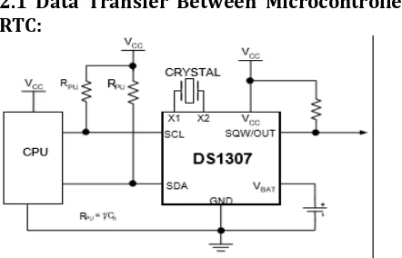
2. INTERFACING AVR WITH REAL TIME CLOCK
The DS1307 serial real-time clock (RTC) is a low power, full binary-coded decimal (BCD) clock/calendar plus 56 bytes of NV SRAM. Address and data are transferred serially through an I2C, bidirectional bus. The clock/calendar provides seconds, minutes, hours, day, date, month, and year information. The end of the month date is automatically adjusted for months with fewer than 31 days, including corrections for leap year. The clock operates in either the 24-hour or 1224-hour format with AM/PM indicator. The DS1307 has a built-in power-sense circuit that detects power failures and automatically switches to the backup supply.
2.1
Data Transfer Between Microcontroller and
RTC:
[image:1.595.314.527.569.720.2]Fig 2.1 Interfacing between RTC and microcontroller
[image:1.595.36.279.575.722.2]© 2017, IRJET | Impact Factor value: 5.181 | ISO 9001:2008 Certified Journal
| Page 3420
The DS1307 can operate in the following two modes:A. Slave Receiver Mode (Write Mode): Serial data and clock are received through SDA and SCL. After each byte is received an acknowledge bit is transmitted. START and STOP conditions are recognized as the beginning and end of a serial transfer. Hardware performs address recognition after reception of the slave address and direction bit. The slave address byte is the first byte received after the master generates the START condition. The slave address byte contains the 7-bit DS1307 address, which is 1101000, followed by the direction bit (R/W), which for a write is 0. After receiving and decoding the slave address byte, the DS1307 outputs an acknowledge on SDA. After the DS1307 acknowledges the slave address + write bit, the master transmits a word address to the DS1307. This sets the register pointer on the DS1307, with the DS1307 acknowledging the transfer. The master can then transmit zero or more bytes of data with the DS1307 acknowledging each byte received. The register pointer automatically increments after each data byte are written. The master will generate a STOP condition to terminate the data write.
B.Slave Transmitter Mode (Read Mode): The first byte is received and handled as in the slave receiver mode. However, in this mode, the direction bit will indicate that the transfer direction is reversed. The DS1307 transmits serial data on SDA while the serial clock is input on SCL. START and STOP conditions are recognized as the beginning and end of a serial transfer .The slave address byte is the first byte received after the START condition is generated by the master. The slave address byte contains the 7-bit DS1307 address, which is 1101000, followed by the direction bit (R/W), which is 1 for a read. After receiving and decoding the slave address the DS1307 outputs an acknowledge on SDA. The DS1307 then begins to transmit data starting with the register address pointed to by the register pointer. If the register pointer is not written to before the initiation of a read mode the first address that is read is the last one stored in the register pointer. The register pointer automatically increments after each byte are read. The DS1307 must receive a Not Acknowledge to end a read.
2.2 Utilities to handle the data transfer:
To set the time for RTC, the utility is RTCset( char * data). It takes in a character string with the format “hours:minutes:seconds:day:day of month:month:year”. For example to set the hour as 8 AM and some arbitrary date, we can send the character string as RTCset(“8841001140516”). Using the parameter, We fetch each value and convert them
into integers by unwrapping their ASCII value is as follows:
(((data[0]-48)<<4)|(data[1]-48)) /*for hours, similar thing is carried out for other parameters*/. What happens in the above case is data[0] points to character ‘8’ whose ASCII value is 56. In order to convert it back to integer value, the ASCII value equivalent to ‘0’ character i,e 48 is subtracted yielding the value 8. Same thing is carried out on data[1] value. The data[0] is actually sent for configuration of storage and part of actual data and data[1] refers to other part of data. After shifting and carrying out the OR operation data stored in binary will be as 10001000. The MSB is clock oscillator enable bit, followed by bit which indicates whether the RTC time should be in 12/24 hour format. 0 indicates 12 hour and 1 indicates 24 hour format. This is followed by AM/PM indication for 12 hour format and 10 hour bit to indicate the higher data nibble for 24 hour format as data is stored in BCD format in the RTC memory. Bit 4 is used to indicate the higher data nibble for 12 hour format. The bits from 0 to 3 are used to indicate the lower data nibble for 12 hour format. This data is then sent via I2C bus. The inverse utility to continuously read data from RTC is RTCRead(char * data), which reads the data byte to the memory pointed by data parameter. Here until the last byte, data is read with acknowledge and a non-acknowledgement is sent by the master after last byte indicating termination for data stream transfer. Each time the data is read to a temporary variable from I2C bus. The higher nibble is retrieved by right shifting the data bits 4 times and adding the value 48 to bring it back to ASCII value in order to display it on the screen. The lower nibble is fetched by masking and adding 48 to obtain the same objective.
temp=readACK(); data[index]=(temp>>4)+48; data[index+1]=(temp& 00001111)+48; /* pseudo code for obtaining the data in the suitable format*/
The formula for setting the master clock rate is as follows: CPU_CLK_FREQUENCY/16+2(TWBR)*4^TWPS. TWBR is the value of TWI bit rate register and TWPS is value of pre-scalar bits
in TWI status register.
3. INTERFACING AVR WITH NOKIA 5510 SCREEN
© 2017, IRJET | Impact Factor value: 5.181 | ISO 9001:2008 Certified Journal
| Page 3421
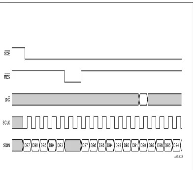
The PCD8544 is manufactured in n-well CMOS technology. [image:3.595.39.238.242.414.2]The DDRAM is a 48 × 84 bit static RAM which stores the display data. The RAM is divided into six banks of 84 bytes (6 × 8 × 84 bits).Each character is made to occupy 5*8 matrix bits. A constant array is defined which contains the display data format of 96 characters, where each character occupies 5 bytes of data. For example { 0x7e,0x11,0x11,0x11,0x7e} represents ‘A’. 0x7e is written at a particular co-ordinate, so the subsequent bye 0x11 is written at the next row relative to the column of the first byte.
Fig 3.1 Transmission of multiple bytes via SPI bus.
3.1 Utilities to handle the Initialization, formatting
data and data transfer
The brightness of the screen is controlled by a duty cycle, for which we make use of the PWM module in the AVR. Fast PWM in inverted mode is made use of at pre-scaler set to 64. The set_dutycycle(unit_8) utility takes in a byte as a parameter and assigns it to OCR0 register. The count is made using the timer till the value matches the OCR0 and as soon as it reaches the voltage is inverted relative to it’s previous extreme.
When the D/C’ pin is set to 1 , the incoming data is treated as data and when it is set to 0 it is treated as instruction. Four different display modes available i,e blank(0x00), all on(0x01),normal(0x04) and inverse(0x05).These can accessed by OR operation with DISPLAY_CONTROL generic code (0x08) and sent via SPI Bus. Send_command(unit_8) and send_data(unit_8) share the same piece of code i.e. selecting the slave and sending the data except manipulating the D/C’ pin to make the driver interpret whether incoming data is actual data or instruction.
The render_sentence_xy(char *,unit_8,unit_8) utility renders
a specific sentence at the particular x and y coordinates given by the user. This first calls the set_cursor_bank(unit_8,unit_8) function which selects the appropriate display bank and points the location at which the sentence need to be displayed. This is achieved by OR operation of x co-ordinate with 0x40 and of y co-ordinate with 0x80, because screen consists of 48 rows and 84 columns and finally sending them as commands. After this each character in the sentence is rendered from the lookup table i,e the constant array till a null character is encountered. For each character the essential 5 bytes is sent to the driver as data.
4. NAVIGATION AND INPUTS
A joystick is made use for navigation who’s four orientation is mapped to four pins of AVR microcontroller and is complemented with two other switches for selecting and de-selecting/back operation. To counter the debouncing issue, the switch state validation routine is made to run each time a timer interrupt occurs due to overflow. The prescaler is set 256. Timer2 which is of 8 bit is made use of this purpose. The MAX_DEBOUNCE value is set as constant, and a counter variable is assigned to each pin which increments if the condition of momentary pressed is met. When the counter reaches its max debounce value, the pin’s input is considered as valid. As the timer interrupt occurs for a very short interval say 270 microseconds, the behind the scene routine operation cant be discerned by the user. The debounce counters for 6 pins is achieved by an array of size 6.
5. WORK FLOW AND PSEUDO ALGORITHM
a) As soon as the embedded application enters the main() function, It carries out the hardware initialisation. This involves setting the direction of input/output ports, screen brightness configuration and displaying a welcome message and also establishing proper SPI communication, The I2C communication configuration where microcontroller sets or receives date and time from RTC(real time clock), Configuration of serial baud rate in order to communicate with the esp8266 Wi-Fi module.
© 2017, IRJET | Impact Factor value: 5.181 | ISO 9001:2008 Certified Journal
| Page 3422
module. A toggle switch is also deployed to switch betweenflash mode i.e. programming mode where code from AVR gets dumped into flash memory of esp8266 via the serial bus , and run mode; where the code dumped is made to run on the 32 bit auxiliary microcontroller residing in the ESP8266 chip.
Fig 5.1 Connection between ESP8266 and UART port of microcontroller.
The Baud rate is set to 115200 bps, with processor running at 11.0592 Mhz. The baud value is calculated by the formula=((F_CPU)/(BAUD_RATE*16UL)-1).
c) Now, it waits input from user. If negation button is pressed, microcontroller goes to sleep mode. In sleep mode the I/O clock is stopped, input buffers will be disabled hence power consumption will be considerably low. In order to trigger it back into normal mode, an interrupt which can’t be ignored INT0 is mapped to the select pin. The interrupt routines will redirect the flow to where it was left before. If select pin is pressed instead, we will be redirected to a routine which allows us to select an application, we wish to run.
d) The applications can be registered in a file which contains an array of structure called APPS. It consists of two attributes: name of the application and a function pointer to store the address of the application code which needs to be invoked. The Top and Down navigation keys of the joystick helps the user to navigate across the options of applications to choose from. After navigating to a particular application option, if a right or left navigation key is pressed; the appropriate application’s function pointer is invoked which shifts the control to that application. Internal pseudo procedure is as follows:
apps[index].pointer(); /* where index is a counter that refers to a particular APP structure instance and pointer() is the function pointer to the application code.
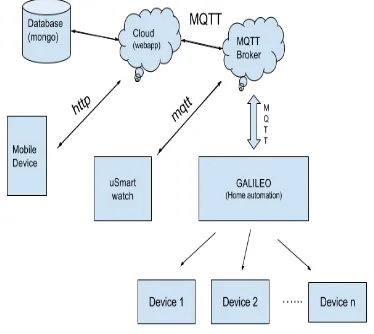
e) one of the application is ‘Home automation control’. This app lets the user to control his numerous appliances in his home. It is built on MQTT protocol for exchange of control data between the watch and the end appliances. The statuses of appliances are mapped to bits in a variable. For Example if Hall-light, ac system, geyser are mapped to bits from MSB to LSB, then the status 101 implies hall-light and geyser is ON whereas AC is OFF. This status information is sent over Wi-Fi (esp8266, with custom firmware which converts serial data into Wi-Fi signal) to a Mosquito Broker, which hosts channels for user to send and receive data using MQTT protocol over a particular long lasting session of TCP connection. Having received the data with QOS and Topic set, it translates to the server location where data needs to routed for controlling. We have made use of node.js server hosted in galileo board connected to Wi-Fi end at home network which unpacks the data from our protocol designed using a python script and to control the appliances accordingly using relay and transistor to boost and connect the AC supply to devices.
[image:4.595.37.263.190.376.2]Ex: d,topic:/ucontrol,data:7 implies ‘111’ in binary indicating that all appliances to be turned on.
Fig 5.2 overview of the architecture
6. OVERVIEW OF MQTT
[image:4.595.354.541.466.633.2]© 2017, IRJET | Impact Factor value: 5.181 | ISO 9001:2008 Certified Journal
| Page 3423
header, variable header and payload. Each MQTT controlpacket has a 2 byte Fixed header. Not all the control packet has the variable headers and payload. A variable header contains the packet identifier if used by the control packet. A payload up to 256 MB could be attached in the packets. Having a small header overhead makes this protocol appropriate for IoT by lowering the amount of data transmitted over constrained networks.
Three QoS for message delivery could be achieved using MQTT:
a) QoS 0 (At most once) - where messages are delivered according to the best efforts of the operating environment. Message loss can occur.
b) QoS 1 (At least once) - where messages are assured to arrive but duplicates can occur.
[image:5.595.328.561.73.237.2]c) QoS 2 (Exactly once) - where message are assured to arrive exactly once.
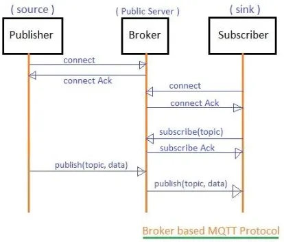
Fig 6.1 Control flow of data and control information in the pub-sub model employing MQTT broker
[image:5.595.42.249.377.553.2]The MQTT broker works on publisher-subscriber architecture where it maintains a table consisting of entries in (name, value) pairs .The names correspond to the topics and the values are a list of subscribers who are subscribed to that corresponding topic. If the broker gets a data or control message for a particular topic, it looks up in the table and finds out which all the subscribers are and what channel has been assigned to each of them. After this, it flushes out the data in those corresponding channels. This serves as a major advantage as clients can reduce the overhead of the controlling and management of data transfer connection processing.
Fig 6.2 Final architecture
7. SOFTWARE TOOLS
1. Avr-gcc and binutils : atmega code compiler and other utilities.
2. Avr-dude: used to flash the code into the memory of the atmega microcontroller.
3. Xtensa-gcc and binutils: code compiler used for esp8266 and binutils.
4. esptool.py : code flash utility for esp8266 module.
5. Esp8266 SDK: used for esp8266 code development aided by API.
6. MongoDB : NOSQL database
7. git client : for source revision control
8. red hat’s openshift platform : cloud hosting.
9. Mosquitto and mosquitto clients : mqtt broker and test utilities.
All the softwares are open source, giving the flexibility to configure it according to the user’s application.
8. CONCLUSION
© 2017, IRJET | Impact Factor value: 5.181 | ISO 9001:2008 Certified Journal
| Page 3424
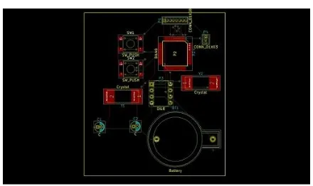
connectivity. Data retrieved by sensors were uploaded to [image:6.595.36.254.162.263.2]database residing in the cloud. The fabrication design has been done where we have employed a 2 layer PCB board. The 3D and 2D view of the PCB is as follows:
Fig 9.1 3D view of PCB
Fig 9.2 2D view of PCB
9. REFERENCES
[1] MQTT Version 3.1.1 Plus Errata 01. Edited by Andrew Banks and Rahul Gupta. 10 December 2015. OASIS Standard Incorporating Approved Errata 01.
[2] Datasheet for screen (PCD8544)
https://www.sparkfun.com/datasheets/LCD/Monochro me/Nokia5110.pdf
[3] Datasheet for Atmega32
http://www.atmel.com/images/doc2503.pdf
[4] Architecture of cloud for IoT
https://developer.ibm.com/architecture/pdfs/IBMClou d-AC-IoTRAOverview-29.pdf
[5] Low Cost Home Automation with ESP8266 and
Lightweight protocol MQTT
[image:6.595.34.254.302.433.2]