Integrated 2-D Optical Flow Sensor
Technical Report - submitted for journal publication in 2004
January 11, 2004
author: Dr. Alan A. Stocker
Member IEEE
Howard Hughes Medical Institute and Center for Neural Science
New York University
4 Washington Place Rm 809 New York, NY 10003-1056 U.S.A.
phone: +1 (212) 992 8752
fax: +1 (212) 995 4011
email: [email protected]
Abstract
I present a new focal-plane analog VLSI sensor that estimates optical flow in two visual dimensions. The chip significantly improves previous approaches both with re-spect to the applied model of optical flow estimation as well as the actual hardware implementation. Its distributed computational architecture consists of an array of locally connected motion units that collectively solve for the unique optimal optical flow estimate. The novel gradient-based motion model assumes visual motion to be
translational, smooth and biased. The model guarantees that the estimation prob-lem is computationally well-posed regardless of the visual input. Model parameters can be globally adjusted, leading to a rich output behavior. Varying the smoothness strength, for example, can provide a continuous spectrum of motion estimates, rang-ing from normal to global optical flow. Unlike approaches that rely on the explicit matching of brightness edges in space or time, the applied gradient-based model as-sures spatiotemporal continuity on visual information. The non-linear coupling of the individual motion units improves the resulting optical flow estimate because it re-duces spatial smoothing across large velocity differences. Extended measurements of a 30x30 array prototype sensor under real-world conditions demonstrate the validity of the model and the robustness and functionality of the implementation.
index: visual motion perception, 2-D optical flow, constraint optimization, gradient descent, aVLSI, analog network, collective computation, neuromorphic, feedback, non-linear smoothing, non-non-linear bias
1
Motivation
a
A
B
C
D
t0 t1
t0 t1>
b
x
v
v
yconstraint lines
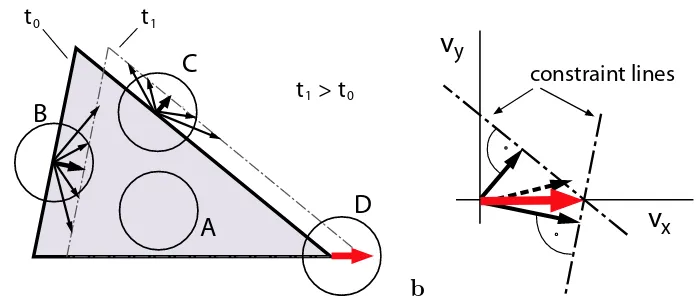
Figure 1: The aperture problem. (a) Translational image motion induces locally ambiguous visual motion percepts. (b) Vector averaging of the normal flow field (dashed arrow) does not lead to the correct global motion. Instead, only the intersection of the constraint lines provides the correct common object motion (bold solid arrow).
architecture, processing power scales with array size, thus keeping the processing speed independent of spatial image resolution. Local visual motion is usually represented by a vector field, referred to asoptical flow. Analog VLSI circuits require significantly less power and silicon area than digital circuits for computational tasks of comparable complexity [1]. Furthermore, time-continuous analog processing matches the the continuous nature of visual motion information. Temporal aliasing artifacts do not occur while they, in contrast, can be a significant problem in clocked, sequential circuit implementations, in particular when limited to low frame-rates [2].
Visual information is – in general – ambiguous and does not allow a unique local in-terpretation of visual motion, a major reason being the aperture problem [3]. A priori
assumptions are necessary in order to resolve the ambiguities. Such assumptions instan-tiate the motion model of the expected visual motion. Thus, the computational task and the resulting quality of the optical flow estimate can vary substantially depending on the complexity of the chosen model. Figure 1a illustrates the aperture problem for a simple mo-tion scene under noise-free condimo-tions. Observamo-tions through apertures showing zero-order (aperture A) or first-order spatiotemporal brightness patterns (apertures B and C) do not allow an unambiguous local estimate of the visual motion. The presence of a higher-order brightness pattern as e.g. the corner of the triangle in aperture D, would allow to uniquely determine the local visual motion without further assumptions, however requiring complex spatiotemporal filters to account for all possible patterns. Alternatively, instead of resolv-ing complex patterns locally, visual information could be spatially integrated, combinresolv-ing the perception through multiple, sufficiently small apertures such that the spatiotemporal
pattern within each aperture can be well approximated to be maximally of first order. Com-bining the constraints imposed by the first-order patterns then ideally leads to the unique and correct estimate of object motion. It is important to realize, that the vector average of the normal flow, that is the optical flow being perpendicular to the first-order pattern ori-entation in each aperture, usually does not coincide with this collective constraint-solving estimate (see Figure 1b). The problem remains to decide how the constraints imposed by the observations at the different apertures are weighted, i.e. which apertures observe a common visual motion source and should be combined. Dynamical grouping processes have been suggested that assign varying ensembles of apertures to different image objects at any time, leading to an individual estimate of visual motion for each ensemble (object) [4, 5, 6, 7, 8]. Although the aVLSI implementation of an optical flow sensor with dynam-ical grouping process has been reported recently [9], such dynamic processes will not be discussed further in this paper. Just note, that spatial integration is a necessary requisite to solve for the correct object motion.
2
Review of aVLSI visual motion sensors
Most of the known aVLSI motion sensors estimate visual motion only along a given single spatial orientation which significantly simplifies the computational problem. They can be classified in methods performing explicit matching in time-domain e.g. [10, 11, 12, 13, 14],
gradient based methods e.g. [15, 16] and implicity matching or correlation based methods, that follow insect vision e.g [17, 18, 19, 20, 21, 22].
Only a few 2-D visual motion sensors have been reported. In the following, theses approaches are briefly reviewed according to their applied motion models. A first class es-timates the direction of normal flow. Higgins and colleagues [23] presented two focal-plane implementations that provide a quantized signal of the direction (8 directions) of normal flow. The two architectures are functional very similar: the occurrence of a brightness edge at a single image location is detected and compared with its re-appearance at neighboring locations. Deutschmann and Koch [24] proposed an approach to estimate the direction of normal flow by multiplying the spatial and temporal derivatives of the brightness distribu-tion in the image. The limited linear range of the applied multiplier circuits impairs the correct directional estimate, leading to an increasing emphasis on diagonal visual motions for increasing stimulus contrasts. The output signal is monotonic in visual speed for a given stimulus contrast but substantially varies contrast.
reported if the time-of-travel of the extracted edges between neighbor motion units matches a pre-set delay time. Since the tuning is very narrow, the sensor is fairly limited and can-not report arbitrary visual velocities without being continuously re-tuned. More practical sensors were reported by Krameret.al.[26], applying explicit matching in the time-domain. Two circuits are presented where the time-of-travel of an brightness edge in the image is measured either by eliciting a monotonic decaying function with arrival of an edge and sam-pling the functions value at the time the edge passes a neighboring pixel, or, by measuring the amount of overlap of two fixed-size pulses of neighboring pixels that each are triggered by the arrival of a brightness edge. A similar approach but different implementation was proposed by Etienne-Cummings et.al [27]. Where as in [26] temporal intensity changes are assumed to represent brightness edges, here, brightness edges are first extracted in the spatial domain before matching was performed in the time-domain. This has the advantage that also very slow speeds can accurately be detected.
None of the above approaches, however, perform spatial integration beyond averaging in order to solve the aperture problem. Tanner and Mead [28] reported a sensor with an array size of 8x8 pixels that provides two output voltages each representing the two components of the global motion vector. But, measured motion data was never explicitly shown and the sensor was reported to be fragile, even under well-controlled laboratory conditions. Nevertheless, it was the first hardware example of a collective computational approach to visual motion estimation. Subsequent attempts [29] failed to result in a more robust implementation. Only in a previous paper [30], we presented a first improvement that also allowed estimation of smooth optical flow besides a global motion estimate. The prototype implementation with a 7x7 array was functional although it was rather limited by its small linear output range. Another recent attempts [31] incorporated segmentation properties into our previous approach but were not able to demonstrate robust behavior under real-world conditions.
The 2-D optical flow sensor reported here represents a significant improvement and further development of all previous approaches, both in terms of the applied motion model as well as its aVLSI implementation. It is the first robust and fully functional sensor of its kind. My recently documented motion segmentation chip [9] shares an identical circuit design for its motion units.
3
Optical Flow Model
For analytical reasons, we define theinputof the proposed model to be the spatiotemporal gradientsEx = ∂x∂ E(x, y, t),Ey = ∂y∂ E(x, y, t), andEt = ∂t∂E(x, y, t) of the brightness
bution E(x, y, t) in the image. We will later discuss the extraction of these spatiotemporal gradients in the actual focal-plane implementation. The model’soutput is the optical flow field v(x, y, t) = (u(x, y, t), v(x, y, t)) that represents the instantaneous estimate of visual motion. To increase readability, space and time dependence will not be explicitly expressed in subsequent annotations although it is implicitly always present.
The applied motion model assumes that the brightness constancy constraint [32] holds and that the optical flow variessmoothlyin space. Following Horn and Schunck [33], these two constraints can be formulated as optimization problem for which the desired optical flow estimate is the optimal solution (see also [34]). However, it can easily be verified that using only these two constraints results in anill-posedestimation problem for particular visual input patterns. Namely, when only zero and first order brightness patterns of equal orientation are present throughout the whole image. It is highly desirable for a physical system such ase.g. an aVLSI sensor that the computational function implemented is always well-posed. Otherwise, the system’s behavior is unpredictable, driven by noise and non-idealities of the implementation. Therefore, the so-called bias constraint is added, expressed as the cost function
B(v) = (u−uref)2+ (v−vref)2, (1)
which weakly biases the optical flow estimate to some predefined reference motion (uref, vref).
The reference motion can be understood as the a priori expected motion in case the visual information content is unreliable or missing. In contrast to similar suggested formula-tions [35, 36, 37], the reference motion is not necessarily assumed to be zero. Much more, it could be adaptive to account for the statistics of its visual environment; the reference motion coulde.g. represent the statistical mean of the experienced visual motion. However, such adaptation mechanisms will not be further discussed in this article.
Combining the model of Horn and Schunck with the additional bias constraint (1), we now formulate the following constraint optimization problem over all nodesi, j in a discrete, orthogonal n×m image space: Given the input Exij, Eyij and Etij and a reference motion
vref = (uref, vref), find the optical flow field vij such that the cost function
H(vij;ρ, σ) = n
X
i=1
m
X
j=1
(Exijuij+Eyijvij+Etij)
2+
ρ((∆uij)2+ (∆vij)2) +σ((uij−uref)2+ (vij−vref)2)
(2)
is minimal 1. The positive parameters σ >0 and ρ ≥0 determine the relative influence of
each constraint.
1(∆x
ij)2= xi−1,j2−hxi+1,j 2
+ xi,j+1−xi,j−1 2h
2
U ρ
C
U σ U U ρC
σ V V V V V VF
F
U U ref i,j i+1,j i,j+1 i,j-1 i,j+1 i+1,j i-1,j i,j ref i,j i,j i,j-1 i-1,jA
B
j= [1...m ]
x y
i= [1...n ]
u
v
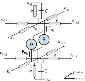
Figure 2: A single unit of the optical flow network.
4
Optical Flow Network
The optimization problem (2) is convex for any given input. Thus, a linear dynamical system that performs gradient descent on the cost function (2) is guaranteed to provide the optimal estimate once it reaches steady-state. Partial differentiation of (2) results in a system of 2n×m linear partial differential equations
˙
uij =−
1
C
Exij(Exijuij+Eyijvij+Etij)−ρ(ui+1,j+ui−1,j+ui,j+1+ui,j−1−4uij)+σ(uij−uref)
,
˙
vij =−
1
C
Eyij(Exijuij+Eyijvij+Etij)−ρ(vi+1,j+vi−1,j+vi,j+1+vi,j−1−4vij) +σ(vij−vref)
(3) with C being a positive constant.
These first-order partial differential equations exactly describe the dynamics of two ac-tively coupled resistive networks. Figure 2 illustrates a single unit of such coupled networks. Identifying the local estimate of optical flow with the voltagesUij,Vij 2, the terms in straight
brackets (3) represent the sum of currents that charges up or down the capacitancesC until equilibrium is reached. Each constraint of the cost function (2) has a physical counterpart: smoothness is enforced by the resistive networks with lateral conductances ρ. The bias
2with respect to some null potentialU0andV0 respectively.
constraint is implemented as the leak conductanceσ to the reference motion represented by the potentials Vref and Uref.
Only the implementation of the brightness constancy constraint needs some active cir-cuitry represented by the “constraint-boxes”[38] Aand B that inject or sink the currents
Fui,j ∝ −Exij(Exijuij+Eyijvij+Etij) and Fvi,j ∝ −Eyij(Exijuij+Eyijvij+Etij), (4)
respectively. These correction currents represent the violation of the constraint and are computed in a cross-coupled feedback loops. We exploit the natural dynamics of a physical system to solve a visual perception problem [39]: The solution of the optimization problem is represented by the steady-state of the analog electronic network. The system is assumed to be in steady-state at any time. This approximately holds if the time-constant of the network is negligible compared to the dynamics of the input. The appropriate control of the node capacitance C and the current levels in the implementation can ensure a close-to-optimal solution for reasonably slow input dynamics. Note, that the dynamics of the network strongly depend on the spatiotemporal energy of the visual input.
The characteristics of the model and therefore the computational behavior of the optical flow network are determined by the relative weight of the three constraints, determined by the lateral and vertical network conductances ρ and σ, respectively. According to the strength of these conductances, the network accounts for different models of visual motion estimation such as normal flow, smooth optical flow or global flow. The presented optical flow sensor allows to globally adjust ρ and σ which is certainly one of its advantages.
5
Circuit Architecture and Implementation
The complete circuit schematics of a single motion unit of the optical flow sensor is shown in Figure 3. Since the input (spatiotemporal intensity gradients) and the output (the compo-nents of the local optical flow vector) can take on positive and negative values, a differential encoding of the variables is applied consistently throughout the circuit: The variables are encoded as the difference of two voltages (or currents). However, referencing the voltages
U+ andV+ to a fixed null potentialV0 substantially reduces the implementation complexity
Vdd Vdd BiasOp BiasVVi1 Vdd Vdd Vdd BiasHR BiasVVi1 Vdd Vdd Vdd Vdd − + Vdd Vdd − + Vdd Vdd
HDtweak- HDtweak+
V
0 BiasHD Vdd Vdd Vdd Vdd Vdd BiasPhA BiasPhFollower Vdd Vdd Vdd VddV
+ BiasVVi2 BiasVVi2 BiasHR Et+ Phx+ Ph0 Phy+Phx+ Phx- Ph
x+ Ph
x-Ph
x-E
t-U
+Fv
-Fv+
Fu + BiasOp − + Phy+
Phy+ Phy+
Ph y-Ph
y-Vdd Vdd
BiasPh
Fu
-C
C
Photoreceptor
Differentiator
HRes circuits
Cascode current mirror
Figure 3: Schematics of a single motion unit.
5.1
Extraction of the brightness gradients
The circuit schematics contains all building blocks of a single unit. At a first processing stage, the spatiotemporal brightness gradients have to be estimated. Each pixel includes a logarithmic, adaptive photoreceptor [40] with adjustable adaptation rate [41].
The temporal gradient is extracted by a hysteretic differentiator circuit [42] providing the currentsEt−,Et+ that represent the rectified temporal derivative. The adjustable source
potentials HDtweak+,HDtweak- allow to control the output current gain of the differentiator.
The spatial derivatives Ex and Ey are estimated as first-order approximation of the
brightness gradients, thus the central difference value of the photoreceptor output of nearest neighbors (P hx+−P hx−) and (P hy+−P hy−) respectively (see schematics in Figure 3). While
continuous-time temporal differentiation avoids any temporal sampling artifacts, discrete spatial sampling of the image brightness significantly affects the visual motion estimate.
Let us consider a simplified, one-dimensional arrangement as depicted in Figure 4a, where a sine-wave grating moving with a fixed velocity v is presented. We describe the brightness distribution in the focal-plane as E(x, t) = sin(kx−ωt) with x, t ∈ R, where
ω = kv and k is the spatial frequency of the projected stimulus. First order approxi-mation of the spatial gradient at location xi thereby reduces to the difference operator
∆xi = (xi+1−xi−1)/2d, where dis the sampling distance (pixel size). Assuming a non-zero
sampling size D (photodiode), the discrete spatial gradient becomes
Ex(xi, t) =
1 2d
1
D
Z xi+d+D/2
xi+d−D/2
sin(k(ξ−vt)) dξ − 1 D
Z xi−d+D/2
xi−d−D/2
sin(k(ξ−vt)) dξ
!
= 2
kDd sin(kd) sin(kD/2) cos(k(xi−vt)). (5)
Similarly, the temporal gradient at location xi is found to be
Et(xi, t) =
∂ ∂t
1
D
Z xi+D/2
xi−D/2
sin(k(ξ−vt)) dξ =−2v
D(cos(k(xi−vt))·sin(kD/2)). (6)
According to (3), the response of a single unit in equilibrium with no lateral coupling (ρ= 0) is expected to approximate normal flow and reduces for one visual dimension to
Vout(xi, t) =−
Et(xi, t)Ex(xi, t) +Vrefσ
σ+Ex(xi, t)2
(7)
Substitution of (6) and (5) into (7) and assuming Vref = 0, we find
Vout(xi, t) =v
kd
sin(kd) ·
cos(kxi−ωt)2
γ+ cos(kxi−ωt)2
with γ=σ k
2d2D2
a
v
k=0.5
k=1 k=1.5
d D
x
i-1x
ix
i+1Brightness
b spatial frequency k [ /d]π
motion response [a.u.]
v
σ=0, δ∈ [0,1]
σ=0.05, δ=1/3
0.03 0.1 1 2
σ=0.05, δ 0 0
Figure 4: Spatial sampling and its effect on the motion response. (a) Spatial sampling of sinusoidal brightness patterns of different spatial frequencies k (given in units of the Nyquist frequency [π/d]) in one visual dimension. (b) The expected response of the optical flow sensor according to (7) as a function of the spatial frequency k of a sinewave stimulus moving with velocityv. The dashed curve is the time-averaged response (σ = 0.05,δ= 1/3).
We now can predict the motion response of a single isolated unit as a function of spatial frequency of the stimulus for different weights of the bias constraint σ as well as different fill-factors δ = D/d. Figure 4b shows the predicted peak output response for different parameter values as a function of the spatial stimulus frequency k, given in units of the Nyquist frequency [π/d]. Note that the response strongly depends on k. Only for low spatial frequencies, the motion output well approximates the correct velocity. For very low frequencies, the local stimulus contrast diminishes and the non-zero σ biases the output response toward the reference motion V0 = 0. As the spatial frequency approaches the
Nyquist frequency, the response increases to unrealistically high values and changes sign at k ∈ Z+[π/d]. Increasing the fill factor reduces the effect, although only marginally for
reasonable values ofδ and smallσ. Clearly, if the bias constraint is not imposed, thusσ = 0, Equation (8) reduces to
Vout =v
kd
sin(kd) (9)
The computation is ill-posed at spatial frequencies k ∈ Z+ and the motion response
ap-proaches ±∞ close to their vicinity. Two things are remarkable: Firstly, D drops out in
the equation which means that the spatial low-pass filtering of the photodiode only affects the motion estimate if the bias constraint is imposed. Secondly, the output (9) does not depend on space nor time. For σ > 0, however, γ is always non-zero and the motion response becomes phase-dependent due to the remaining frequency terms in (8). As a consequence, the time-averaged motion response over the duration of a complete stimulus cycle is always less than the peak response as shown in Figure 4b. Phase-dependence is a direct consequence of the bias constraint. However, spatial integration of visual information due to collective computation in the optical flow network allows to partially overcome the phase-dependent response of a single unit.
Note, that the first-order difference approximation of the spatial brightness gradients in two visual dimensions is not rotationally invariant. Unfortunately, more elaborate gradient approximations [43] are not feasible for a compact focal-plane implementation.
5.2
Wide-linear range multiplier
The design of the multiplier circuit needed to compute Exu and Eyv respectively, is
cru-cial for a successful aVLSI implementation of the optical flow network. Being part of the recurrent feedback loops that generate the error-correction signalsFu and Fv, the demands
on the multiplier circuit are high. It has to operate in four quadrants, providing a wide linear output-range with respect to each multiplicand. Offsets should be minimal because they directly impose offsets in the optical flow estimate. Furthermore, the design needs to be compact in order to allow a small pixel size. The original Gilbert multiplier [44] meets these requirements fairly well, with the exception of its small linear range when operated in sub-threshold. In above-threshold operation, however, its linear range is significantly increased due to a transconductance change of the individual differential pairs [45].
The multiplier circuit proposed here, shown in detail in Figure 5a, embeds a Gilbert multiplier in an additional outer differential pair. The idea is to operate the Gilbert mul-tiplier above-threshold to increase the linear range but in addition, to rescale the output currents to sub-threshold level such that the current levels in the feedback loop match. The scaling is approximately linear, thus
Iout =Iout+−Iout− ≈
Ib2
Ib1
Ioutcore, (10)
if κn ≈ 1, where 1/n is the ideality factor3 of the diodes and κ is the slope factor of
the nFETs in the embedding differential pair. Using the base-emitter junction of bipolar transistor with base and collector connected to a common reference potential ensures an
3Shockley equation: I
a
Vdd
V2
Iout - Iout +
V3
V3 V
4 Vdd
V1
I+ I
-Ib1
Ib2
Vb1
Vb2
D1 D2
b
0.2 0.4 0.6 0.8 1
10 10 10 10 10 -12 -10 -8 -6 - 4
emitter current I
E
[A]
base -emitter voltage VBE [V] MOS bipolar n=1.026
generic bipolar n=1.033
10 -2
c
-1 -0.5 0 0.5 1
-4 -2 0 2 4x 10
-9
∆VA differential input [V] Iout
[A]
d
-1 -0.5 0 0.5 1
-4 -2 0 2 4x 10
-9
differential input ∆VB [V]
Iout
[A]
Figure 5: Wide linear-range multiplier. (a) Circuit schematics. (b) The measured emitter currents for a native npn-bipolar transistor and the vertical pnp-bipolar of a pFET. (c) Measured output currents of the wide linear-range multiplier as a function of the applied input voltage at the lower differential pair ∆VA =V2−V1. Each curve represents the output
current for a fixed differential voltage ∆VB =V4−V3 =[0, 0.05, 0.1, 0.15, 0.2, 0.3, 0.4, 0.5,
0.75 V]. (d) Same as c but now sweeping the upper differential pair input ∆VB.
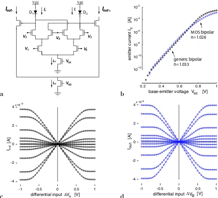
ideal (n = 1) behavior [46] which has been verified by the measurements shown in Figure 5b. Also, the voltage drop across the diodes is such that the gate voltage of the outer nFETs are typically within one volt below Vdd, meaning that their gate-bulk potentials are large.
At such levels, κ asymptotically approaches unity because the capacitance of the depletion layer becomes negligibly small compared to the gate-oxide capacitance. Thus, κn≈ 1 and
we can safely assume a linear scaling of the multiplier output current.
Base-emitter junctions can be exploited either using native bipolar transistors in a gen-uine BiCMOS process or the vertical bipolar transistors in standard CMOS technology. In practice, however, it is necessary to use a native BiCMOS process in order to implement the multiplier circuit correctly: Figure 5b displays the measured base-emitter voltages VBE
as a function of the applied emitter currentIE for both, a vertical pnp-bipolar transistor in
a typical p-substrate CMOS process and a native npn-bipolar transistor in a genuine BiC-MOS process. At current levels above 1 µA, however, the vertical bipolar starts to deviate significantly from the desired exponential characteristics due to high-level injection caused by the relative light doping of the base (well) [46]. This occurs already at a current level that is significantly below the range where the multiplier core is preferably operated at. The exponential regime of the native bipolar, however, extends up to 0.1 mA. Although a CMOS implementation of the diodes is desirable to avoid the more complex and expensive BiCMOS process, it would severely impair the linear scaling (10).
Figure 5c and d show the measured output of the multiplier for sweeping either of the two input voltages. For the applied bias voltages, the linear range is approximately ±0.5 V and slightly smaller for the upper differential input. Note, that the measurements were obtained from a test circuit with identical layout to the one within each pixel. Offsets are small. The circuit is compact and allows to control the linear range and the output-current level independently by the two bias voltages Vb1 and Vb2. The disadvantages are
the increased power consumption caused by the above-threshold operation and the need for BiCMOS technology.
5.3
Output conductance of the feedback-loop
Consider the current equilibrium at one of the capacitive nodes in Figure 2. In steady state, we assume all currents onto this node to represent the deviation to the different constraints according to (3). To be completely true, this would require the feedback current to be generated by ideal current sources A and B. However, the small but present output con-ductance of the feedback node causes some extra current that shifts the current equilibrium. This output conductance can be understood as imposing a second bias constraint on the estimation problem. It biases the capacitive node to a reference voltage that is intrinsic and depends on various parameters like the strength of the feedback current or the Early voltages of the transistors. In general, this reference voltage is not identical withV0. Thus,
the superposition of the two bias currents has an asymmetric influence on the final motion estimate. Since the total correction currents are typically weak, the effect is significant.
as possible. The applied cascode current mirror circuit reveals a substantial decrease in output conductance compared with a simple current mirror used in previous related imple-mentations [28, 29, 30]. Neglecting any junction leakages in drain and source, we find the total output conductance at the individual capacitive nodes to be
go =goN +goP =
F+· UT
VE,N1 VE,N2
+ F−· UT
VE,P1 VE,P2
, (11)
where F+−F− is the total feedback current, UT the thermal voltage and VE,X the Early
voltages of the different transistors in the cascode current mirror (see box in Figure 3).
5.4
Effect of Non-Linearities
Gradient descent on the cost function (2) defines a system of coupled, but linear partial differential equations. However, a linear translation into silicon is hardly possible. In the following, some important non-linearities of the implementation and their effect on the optical flow estimate are discussed.
5.4.1 Saturation in the feedback-loop
The first important non-linearity is caused by the saturation of the multiplier circuit in the feedback loop. As shown in Figure 5, the output current saturates for larger input voltages. What does this mean in terms of the expected motion output of a single motion unit?
For the sake of illustration, we once more assume a one-dimensional array of the optical flow network. Furthermore, we disable all lateral connections and neglect the bias constraint (ρ = 0, σ = 0). Then, for given non-zero brightness gradients, the circuit ideally satisfies the brightness constancy constraint
Exu+Et = 0. (12)
Now, assume that the multiplication Exuis replaced by f(u)|Ex with Ex constant, where f
describes the saturating output characteristics of the proposed multiplier circuit. For reasons of simplicity we assume the output of the multiplier core Icore
out to follow a simple sigmoidal
function tanh(u) which is only qualitatively correct [45]. We can rewrite the multiplier output (10) as f(u)|Ex = cEx Ib2/Ib1tanh(u), where the constant cEx is proportional to a
given Ex. Since f(u) is one to one, we can solve (12) for the motion response and find
u= f−1(−Et) = −artanh(
Ib1
Ib2
Etc−Ex1) . (13)
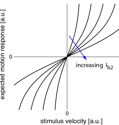
Figure 6 illustrates the expected motion response according to different values of the bias current Ib2. We see that the motion output over-estimates the stimulus velocity the more
0 0
stimulus velocity [a.u.]
expected motion response [a.u.]
increasing Ib2
Figure 6: Expected motion response due to saturation of the multiplier circuit. The figure qualitatively shows the expected speed tuning curves according to (13). The different curves correspond to different values of the bias current Ib2.
the multiplier circuit saturates and finally would end up at the voltage rails. The more the output of the multiplier circuit is below the true multiplication result, the more the feedback loop over-estimates u in order to make the equilibrium (12) hold. Considering the correct characteristics of the real multiplier circuit, the response will differ from Figure 6 insofar as the linear range is increased and the saturation transition is sharper and more pronounced. Nevertheless, Figure 6 illustrates the qualitative response behavior nicely. Increasing Ib2
decreases the slope of the motion response. Thus, the bias current of the outer differential pair acts as gain control that allows to match the limited linear output range to the expected maximal motion range.
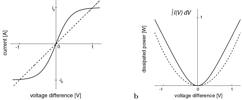
5.4.2 Non-linear bias conductance σ
The quadratic measure of the bias constraint in the cost function (2) results in a constant conductance σ and therefore an ohmic bias current. Sufficiently low and compact ohmic conductances, however, are difficult to implement in CMOS technology. Instead, the bias constraintis imposed by the transconductance gmof a simple amplifier circuit (see Figure 3).
Its characteristics are ideally given as
I(∆V) =Ibtanh(
κ
2UT
with Ib being the bias current controlled by the voltage BiasOP, UT the thermal voltage
and κ the common slope factor. Figure 7a illustrates the output of a saturating resistor according to (14); the transconductancegm= 2IUbκT characterizes the small ohmic regime and
the bias current Ib determines the saturation current level of the circuit.
a
-1 0 1
voltage difference [V]
current [A]
-I b I
b
b
-1 0 1
1
voltage difference [V]
dissipated power [W]
∫ I(V) dV
Figure 7: Ohmic versus saturating resistances. (a) The characteristic curves for an ohmic (dashed line) and a saturating resistance. (b) The electrical co-contents (integrals).
Changing the resistance from a linear to a saturating behavior changes the bias con-straint (1) from a quadratic toward an absolute-value function (Figure 7b), precisely given as the electrical co-content. From a computational point of view, this implies that the optical flow estimate is no longer penalized proportionally to the size of its components. Rather, beyond the small ohmic regime, a constant bias current is applied. Therefore, the bias constraint has a subtractive rather than a divisive effect on the optical flow estimate. As discussed earlier, it seems reasonable to strengthen the bias constraint locally according to the degree of ambiguity. Only, the degree of ambiguity is not at all reflected by the ampli-tude of the motion estimate which is the only information available for the bias conductance. Thus, it is most sensible to penalized the motion estimate independently of its size, which actually means to apply a constant bias current. As we will see later, the non-linear bias conductance significantly improves the output behavior of the optical flow sensor for low contrast and low spatial frequency stimuli compared to a quadratic formulation of the bias constraint as proposed by [37, 35]. Global asymptotic stability of the optical flow network is ensured since the cost function remains convex [45].
5.4.3 Non-linear smoothing of the optical flow
The smoothness constraint is enforced by HRes circuits [42] that have an equivalent charac-teristics as the transconductance amplifier (14) shown in Figure 7. The saturation current level is controlled by the bias voltage BiasHR. As a consequence, the squared differences
of the optical flow components in the cost function (2) have to be replaced by the total dissipated power, thus e.g.
(∆xij)2 ⇒
∆xx ij
Z
0
I(V) dV +
∆xyij
Z
0
I(V) dV = log(cosh(∆xxij)) + log(cosh(∆xyij)). (15)
As the bias constraint, the smoothnes constraint turns from a quadratic (for small volt-age differences) to an absolute-value cost function. Saturating resistors privilege smoothing across small voltage differences, thus between image locations that show only little differ-ences in the components of their optical flow vectors. If the difference becomes too big, the smoothing conductance is continuously reduced in proportion to the local gradient of the optical flow components. Consequently, smoothing is reduced at boundaries of different mo-tion sources where the optical flow is likely to differ. Thisimproves the optical flow estimate compared to applying a linear smoothing conductance. Because the non-linear smoothing is independent in each component of the optical flow estimate, the smoothing is not rota-tionally invariant but rather slightly increased for visual motion along the diagonal of the intrinsic coordinate frame. In contrast to line-processes,e.g. resistive fuses circuits [47], the above non-linear smoothing conductances preserve the convexity of the cost function (2), thus ensures global asymptotical stability.
6
Sensor Measurements
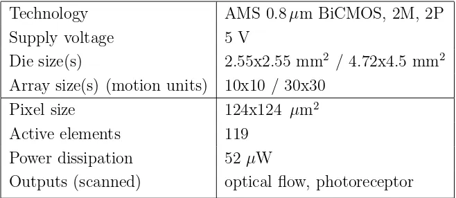
In the following, we will present and discuss measurements gathered of two implementations of the proposed sensor, both sharing an identical pixel design and only differing in their array size. Characterization of the sensors are exclusively based on measurements form the smaller array while the flow fields shown in the end are recorded from the larger array. Specifications are as indicated in Table 1.
For all measurements, the stimuli were directly projected onto the sensor via an optical lens system. They were either generated electronically and displayed on a computer screen, or were physical moving objects. The measured on-chip irradiance during all experiments was within one order of magnitude with a minimal value of 9 mW/m2 for low contrast
Technology AMS 0.8µm BiCMOS, 2M, 2P
Supply voltage 5 V
Die size(s) 2.55x2.55 mm2 / 4.72x4.5 mm2
Array size(s) (motion units) 10x10 / 30x30
Pixel size 124x124 µm2
Active elements 119
Power dissipation 52µW
Outputs (scanned) optical flow, photoreceptor
Table 1: Sensor specifications.
in the order of a few milliseconds [48]. This is sufficiently fast with respect to the applied stimulus speed in those particular measurements. Unless indicated differently, the bias voltages were all sub-threshold. The shown motion output signals are always referenced to the null-potential V0.
6.1
Response characteristics
Moving sinewave and squarewave gratings were applied to characterize the motion response for varying speed, contrast and spatial frequency of the gratings. Furthermore, the orienta-tion tuning of the optical flow sensor and its ability to report the intersecorienta-tion-of-constraints estimate of visual motion are tested. The presented data in this section constitute theglobal
motion signal, thus the unique, collectively computed solution provided by all units of the optical flow sensor. Unless indicated differently, each data point shown in the following figures represents the mean value of 20 single measurements, each being the output voltage time-averaged over one stimulus cycle
6.1.1 Speed tuning
Figure 8a shows the speed-tuning of the optical flow sensor to a moving sinewave and a squarewave grating. Negative speed values indicate motion in the opposite direction. The output is almost identical for both visual stimuli. It clearly shows the qualitatively predicted behavior due to the saturation of the multipliers in the feedback loop (compare to Figure 6). The tuning is linear in a range of approximately ±0.5 V as indicated by the dash-dotted lines for above-threshold operation of the multiplier core (BiasVVI1 = 1.1 V). Beyond the
linear range, the output quickly increases/decreases and finally hits the voltage rails on either side. In contrast to our previous qualitative analysis (13), the measured responses
reveal a pronounced linear-range and a sharper transition to the super-linear behavior.
a
-400 -200 0 200 400
-0.6 -0.4 -0.2 0.2 0.4 0.6
stimulus speed [pixel/sec]
motion output [V] sinewave squarewave b
-1000 -500 0 500 1000
-0.8 -0.6 -0.4 -0.2 0 0.2 0.4 0.6 0.8
stimulus speed [pixels/sec]
motion output [V]
0.00441 0.00205 0.00104 0.00054 0.00028 linear gain [V*sec/pixel]
sinewave
c
-4000 -2000 0 2000 4000
stimulus speed [pixels/sec]
motion output [V]
-0.6 -0.4 -0.2 0 0.2 0.4 0.6 sinewave d
-1000 -500 0 500 1000
stimulus speed [pixels/sec]
motion output [V] squarewave 0.00411
0.00204 0.00104 0.00054 0.00028 linear gain [V*sec/pixel]
-0.6 -0.4 -0.2 0 0.2 0.4 0.6 0.8 -0.8
Figure 8: Speed tuning of the optical flow sensor. (a) Measured time-averaged speed tuning of the optical flow sensor to a moving sinewave and squarewave grating (spatial frequency 0.08 cycles/pixel, contrast 80%). (b) Speed tuning for a moving sinewave grating for different values of the multiplier bias voltage (BiasVVI2 = [0.5, 0.53, 0.56, 0.59, 0.62 V]). (c)
Output in the low gain limit (BiasVVI2 = 0.67 V). (d) Same as b but squarewave gratings.
Values in inlets indicate the measure linear response gains.
Figures 8b,d illustrate how the biasing of the feedback multiplier affects the sensitivity of the optical flow sensor: Increasing the voltage BiasVVI2 leads to a smaller output gain
a
0 0.2 0.4 0.6 0.8 1
0.05 0.1 0.15 0.2 0.25
stimulus contrast
motion output [V]
sinewave squarewave
b
0 0.2 0.4 0.6 0.8 1
0.05 0.1 0.15 0.2 0.25
motion output [V]
quadratic dependence
stimulus contrast
Figure 9: Contrast dependence of the motion output. (a) The motion output is measured as a function of stimulus contrast for sinewave and squarewave gratings. (b) Increasing the bias voltage BiasOP = [0.15, 0.23, 0.26, 0.29, 0.32, 0.35, 0.45 V] leads to an increased
contrast dependence of the motion output, here measured for sinewave grating stimuli.
represent the linear fits to the individual measurements. The linear gain scales by a factor of one half for a fixed increase in bias voltage BiasVVI2 by 30 mV (see measured gain values in
inlets), and thus is inversely proportional to the bias current (10). Comparing the measured responses to sinewave (Figure 8b) and squarewave gratings (Figure 8d) did not reveal any significant differences (see slope values in inlets). Setting BiasVVI2 high (0.67 volts) allows to
measure speeds up to 5000 pixels/sec. However, the response becomes slightly asymmetrical as shown in Figure 8c.
6.1.2 Contrast dependence
The output of the optical flow sensor depends continuously on stimulus contrast. Figure 9a shows the output voltage as a function of stimulus contrast 4 for moving sinewave and
squarewave grating stimuli with identical spatial frequency (0.08 cycles/pixel)and constant speed (30 pixels/sec). The lower the contrast, the more dominant is the influence of the bias constraint, forcing the responses toward the reference voltage V0.
Below a critical contrast value of about 0.3, the output signal continuously decreases towards the zero reference motion V0 with decreasing contrast. The squarewave stimulus
shows a slightly sustained resistance against the drop-off. A least-square fit is applied ac-cording to (7) for the response to the sinewave stimulus. Although it describes the overall response well, the fit gets considerably incorrect around the critical contrast value. The
mea-4contrast measure: (E2−E1)/(E1+E2)
sured output curves rise faster and exhibit a more extended plateau towards lower contrast than the fit. Thisimproved output behavior originates from the non-linear implementation of the bias conductance: The effective conductance decreases with increasing motion out-put signal while (7) assumes a constant σ that leads to a stronger bias at high contrast. Figure 9b shows the influence of the total bias strength on the contrast tuning using the same sinewave grating stimuli as before. Increasing values of the voltage BiasOP lead to
a contrast dependent output over the complete contrast range. For high values of BiasOP
the bias conductance dominates the denominator in (7) and the motion estimate becomes quadratically dependent on contrast: It reduces to the multiplication of the spatial and temporal brightness gradients, hence v ≈ ExEt. In fact, such simple spatiotemporal
gra-dient multiplication makes the costly feedback architecture of the circuit obsolete and can be implemented in a compact feed-forward way [15, 16] as mentioned before. The expected quadratic dependence can be observed in Figure 9b only for very low contrast, because the Gilbert multipliers computing the product of the spatial and temporal gradient saturate for higher contrast levels.
6.1.3 Spatial frequency tuning
The third stimulus parameter tested was spatial frequency. Moving sinewave and square-wave gratings (80% contrast, 30 pixels/sec) of various spatial frequencies were applied. Figure 10a shows the motion output of the optical flow sensor to sinewave and squarewave gratings as a function of spatial frequency.
The waveform difference does not have a significant effect on the output. A least-square fit according to (7) was performed on the response to the sinewave grating for frequencies
k < 0.75. For spatial frequencies k < 0.06, the locally measured spatial gradients on the chip surface are very low and thus the bias constraint dominates and enforces the reference motion. Again, we recognize a significant deviation from the fit caused by the non-ohmic bias conductance. It extends the range for correct motion estimation for low frequencies 0.06 < k < 0.2. As spatial frequencies become high (k > 1), the response curves rapidly drop below zero and remain small negative. The deviation from the predicted response, where large negative values occur as the spatial period drops below the double inter-pixel distance d, resulted from the non-optimal test setup that did not allow to project high spatial frequency stimuli with sufficiently high local contrast onto the focal plane.
The strength of the bias voltage BiasOPaffects the amplitude of the motion output as well
as the spatial frequency for which the motion response is maximal as shown in Figure 10b. Recall, that increasing BiasOP decreases the motion output the more, the smaller the local
a
0.03 0.1 1
0 0.2 0.4 0.6
motion output [V]
spatial frequency k [π/d]
sinewave squarewave
b
0.03 0.1 1
spatial frequency k [π/d]
0 0.2 0.4 0.6
motion output [V]
Figure 10: Spatial frequency tuning (a) The spatial frequency response was measured for a sinewave and squarewave grating moving with constant speeds. Spatial frequencyk is given in units of the Nyquist frequency [π/d]. For frequencies k < 1, the response follows closely the expected response (fit according to 8). The non-linear bias conductance extends the range for accurate estimation for low spatial frequencies (gray area). (b) Increasing the bias voltage BiasOP = [0.1, 0.15, 0.2, 0.25, 0.30, 0.35, 0.40 V] reduces the overall response
and shifts the peak response.
for which the motion output is maximal shifts towards this value with increasing values of BiasOP.
6.1.4 Spatial integration
The ability to accurately estimate two-dimensional visual motion is a key property of the presented optical flow sensor. Figure 11a shows the orientation tuning of the optical flow sensor when presented with an orthogonal plaid stimulus. The output fits well the theoret-ically expected sine and cosine functions.
The optical flow sensor approximately solves the aperture problem for a single moving object on a non-structured background. To demonstrate this, we biased the sensor to com-pute global motion (BiasHR = 0.8 V). Then, a high contrast visual stimulus was presented
that consisted of a dark triangle on a light background, moving in either of the four cardi-nal directions. The triangular object shape requires the intersection-of-constraints solution in order to achieve the correct estimate of object motion. Figure 11b shows the applied stimulus and the global motion estimates of the sensor for a constant positive or negative
a
0 90 180 270 360 -0.4
-0.3 -0.2 -0.1 0 0.1 0.2 0.3 0.4
angle φ [degrees]
motion components [V]
U V
b
-0.5 -0.25 0 0.25 0.5
-0.25 0 0.25 0.5
V [V]
increasing bias constraint
U [V] vector average
Figure 11: Solving the Aperture problem. (a) The optical flow sensor exhibits the expected cosine- and sinewave tuning curves for the orthogonal motion components U and V. The sinusoidal plaid stimulus (spatial frequency 0.8 cycles/pixel, contrast 80%) was moving at a velocity of 30 pixels/sec. (b) The time-averaged output of the optical flow sensor is shown for a triangular object moving in orthogonal directions. The optical flow sensor approximately solves the aperture problem. Data points along each trajectory correspond to particular bias voltages BiasOP = [0, 0.1, 0.15, 0.2, 0.25, 0.3, 0.33, 0.36, 0.39, 0.42, 0.45,
0.48, 0.51, 0.75 V].
object motion in the two orthogonal directions. Each data point represents the estimate for a particular value of the bias conductance. For BiasOP < 0.25 V, the optical flow
sen-sor almost perfectly reports the true object motion in either of the four tested directions although with a small asymmetry in the speed estimate. The non-perfect integration with a directional deviation of less than 10 degrees is the result of the remaining intrinsic output conductance. Note, that a vector average estimate would lead to a deviation in direction of 22.5 degrees for this particular stimulus. As BiasOPincreases, the reported speed decreases
rapidly while the direction of the global motion estimate resembles more a vector average estimate (see arrows in Figure 11b).
6.1.5 Array offsets
a U V
b
-0.6 -0.4 -0.2 0 0.2 0.4 0.6 5
10 15 20 25 30 35 40
output voltage [V]
number of units
V
U
Figure 12: Flow field offsets. (a) The measured time-averaged optical flow for uniform visual motion. (b) Histograms for both components of the optical flow vectors with mean values of U = 0.25 V and V = −0.24 V and standard deviations of Ustd = 0.09 V and
Vstd = 0.04 V respectively.
the bias settings were chosen such that the output values are clearly within the linear range of the optical flow units to prevent any distortion of the output distribution due to the expansive non-linearity of the multiplier circuits.
Figure 12a shows the resulting time-averaged (20 stimulus cycles) optical flow field. It reveals some moderate offsets between the optical flow vectors of the different units in the array. However, these units seem to be located preferably at the array boundaries where device mismatch is usually pronounced due to asymmetries in the layouts. Because motion is computed component-wise, deviations due to mismatch are causing errors in speed as well as orientation of the optical flow estimate. Figure 12b shows the histogram of the output voltages of all motion units. Very similar results were found for other chips of the same fabrication batch. The outputs consistently approximate normal distributions as long as the motion signals are within the linear range of the circuit which is in agreement with randomly induced mismatch due to the fabrication process.
The above offset values are for completely isolated motion units. Already weak cou-pling among the units noticeably increases the homogeneity of the individual responses and therefore reduces the offsets.
6.2
Flow field estimation
In the following, sampled optical flow fields of the 30x30 array implementation are presented. On-chip scanning circuitry allows to simultaneously read-out the optical flow estimate
agesU+,V+) as well as the photoreceptor voltage at each pixel. Scanning was performed at
67 frames/sec (100kHz clock frequency) but can be as high as 1000 frames/sec before the cut-off frequency of the follower based scanning circuitry starts to significantly impair the signals. The following results represent the sampled output of the optical flow sensor pre-sented with real-world stimuli under typical indoor lightning conditions. Each flow vector is defined by the local voltage signals U+, V+ referenced a null potentialV0.
a b
c d
Figure 13: Varying smoothness of the optical flow estimate. (a) The photoreceptor image. (b-d) Optical flow samples for increasing effect of the smoothness constraint (BiasHR=[0.25,
0.38 and 0.8 V]).
Figure 13 demonstrates how a different biasing of the HRes circuits controls smooth-ness. The same ’triangle’ stimulus as in Figure 11b was presented, moving from right to left with constant speed. Optical flow was recorded for three different smoothness strengths and snapshots are shown when the object passed the center of the visual field. Figure 13a represents the photoreceptor output voltages while (b-d) display the flow fields according to increasing values of BiasHR. For low values, spatial interaction amongst motion units is
becomes smoother and finally represents an almost global estimate that well approximates the correct two-dimensional object motion.
Finally, Figure 14 shows a sampled sequence of the optical flow sensor’s output for a ’natural’ real-world scene. The sensor is observing two tape rolls passing each other on a office table from opposite direction. Again, each frame is a snap-shot and consists of a gray-scale image encoding the photoreceptor output voltages overlaid with the estimated optical flow field. The optical flow estimate well matches the qualitative expectations according
a b c
d e f
g h i
Figure 14: Sampled output of the 2-D optical flow sensor watching a real-world scene.
to our previous analysis. Rotation of the rolls cannot be perceived because the spatial
brightness structure on their surface is not sufficient. The flow fields are mildly smooth leading to motion being perceived e.g. in the center-hole of each roll. Note, that the chosen value of the smoothing conductance (BiasHRes = 0.41 V) does not prevent everywhere the
optical flow estimate from being affected by the aperture problem: at the outer borders of the rolls, the flow vectors tend to reflect normal flow. However, for regions for which the smoothing kernel combines image areas of differently orientated spatial gradients (e.g. the center region of the rolls), the aperture problem does not hold and the sensor provides the perceptually correct estimate of visual motion.
The tape rolls sequence demonstrates another interesting behavior of the sensor; the op-tical flow field seems partially sustained and trailing the trajectory of the rolls (see e.g. the optical flow field on the left-hand side in Figure 14c), indicating a long decay time-constant of the optical flow signal. As we have previously seen, the total conductance (11) at the feedback node of each motion units is not constant and is given mainly by the transcon-ductance of the feedback loop and the bias contranscon-ductance5. In the tape rolls sequence, the
background and the table is unstructured revealing almost no spatial brightness gradients. Thus, the transconductance of the feedback loop is dropping low, once the high contrast tape rolls boundary has passed, making the time-constant long because it is now solely de-termined by the bias conductance ρ – which is ideally small. As counter-example, consider the situation after the occlusion of the two tape rolls: there is almost no trailing expansion of the flow field right after occlusion (Figure 14f) when the high-contrast back edge of the second roll immediately induces new motion information6 (high correction currents →high
transconduction). In subsequent frames (Figures 14g-i) the trailing flow field is continuously growing again.
As expected from its implied smooth motion model, the optical flow sensor cannot resolve occlusions where multiple motion sources are present in the same spatial location. In this particular sequence with opposite translational motion sources, the motion estimate cancels at occlusions (see Figure 14d and e).
7
Discussion
The here presented optical flow sensor is an example of an aVLSI implementation of dis-tributed and parallel processing sensory system [49] working in continuous-time. The nearest-neighbor connected array of motion units applies recurrent feedback in order to
5neglecting the smoothness conductance
6note, that a static background can provide motion information (zero motion) as long as it has spatial
correct the common estimate of visual motion according to the local visual information with respect to its built-in internal motion model. Such error coding and adaptation strat-egy is also believed to be pursued by biological neural systems [50]. From a mathematical perspective, the optical flow sensor solves a constraint optimization problem; it has to find the optical flow estimate that best matches the visual information with respect to the im-plicit model. To my knowledge, the sensor is the first functional aVLSI implementation following such strategy. It proves that there is no conceptual reason why such an approach cannot be successfully implemented in aVLSI known for its inherent susceptibility to device mismatch and noise.
The optical flow sensor embeds a motion model that has advantages compared to previ-ously reported computational models of visual motion estimation. The bias constraint leads to a robust system and a computationally rich behavior and has been shown to account for many of the known illusionary percepts of human visual motion [37]. However, the novel
non-quadratic form of the bias constraint caused by the intrinsic non-linear implementa-tion of the bias conductance improves the performance compared to comparable, quadratic formulations [35, 36, 37]; the visual motion estimate is less biased for high contrast stimuli without sacrificing robustness (see e.g. Figure 10a).
Another novel feature of the model is its dynamical properties. The non-zero time-constant of the optical flow sensor leads to the integration of visual motion information over time. Since the time-constant depends on the spatio-temporal energy and thus on the con-fidence in the visual information present, the actual temporal integration window becomes large for weak and short for reliable visual input (see Figure 14): At any time the model assumes the optical flow to change smoothly over time with an integration window adapted to the confidence and thus the signal/noise ratio of the visual input. Recent recordings of the dynamical properties of primate’s visual motion system reveal some similarity with biological systems: Pack and Born[51] reported that pattern selective cells in the visual motion area MT of the macaque monkey are preferably tuned to component motion in their initial response phase and only establish their preference for pattern motion after some la-tency. This is consistent with the gradient-descent dynamics of the optical flow sensor. It also reports initially an estimate that is biased toward the normal flow and continuously approaches the correct pattern motion estimate (results not shown). However, such similar-ities shall not be over-emphasized. Rather, the similarsimilar-ities to these highly evolved biological visual motion systems support the soundness of the presented approach. The optical flow sensor is at most a functional model for biological visual motion processing.
A few reported examples already demonstrate the potential of the sensor for smart visual interfaces [52] or robotics applications [53], in particular when tuned to provide
a global optical flow estimate. The resulting low dimensionality of a global optical flow estimate eliminates the need for high transmission bandwidth and complex interfaces to further processing stages, allowing the construction of simple yet powerful systems. Other applications for surveillance and navigation tasks are certainly imaginable.
The network architecture and thus the motion model applied can be further evolved by including mechanisms that locally control the conductances σij(t) and ρij(t). This could
allow a much richer, more object related computational behavior of the system [45]. Some focal-plane implementations of such network architectures have been reported where the local smoothness conductances σij(t) are adapted to limit motion integration to locations
restricted to individual motion sources [9]. Further research has to be conducted, however, in particular with respect to the necessary separation of more complex systems onto multiple chips. The local control of the bias conductance ρij(t) would also allow interesting
atten-tionally guided visual motion processing. Motion units not belonging to the attentional focus could be suppressed by increasing ρij, thus literally shunting the unit. We know that
such attentional inhibition is involved in the processing of visual motion in area MT [54], for example. Although in detail not biological plausible, such extended aVLSI systems of the optical flow sensor would allow to study in a more systematic way the bottom-up and top-down interplay in a real-time perceptional system.
Acknowledgments
This article presents work over the last few years that was exclusively conducted at the Institute of Neuroinformatics INI7. I want to thank in particular the late J¨org Kramer and
all other members of the hardware group of INI under the lead of Rodney Douglas for help and support. The author thanks Eero Simoncelli, Patrik Hoyer and Giacomo Indiveri for helpful comments on the manuscript. Chip fabrication was done through the multi-project-wafer service kindly offered by EUROPRACTICE. Funding was largely provided by ETH Z¨urich (research grant no. 0-23819-01).
References
[1] C. Mead, “Neuromorphic electronic systems,” Proceedings of the IEEE, vol. 78, no. 10, pp. 1629–1636, October 1990.
[2] P. Nesi, F. Innocenti, and P. Pezzati, “Retimac: Real-time motion analysis chip,” IEEE Trans. on Circuits and Systems - 2: Analog and Digital Signal Processing, vol. 45, no. 3, pp. 361–375, March 1998.
[3] E. C. Hildreth,The Measurment of Visual Motion. MIT Press, 1983.
[4] D. Murray and B. Buxton, “Scene segmentation from visual motion using global optimiza-tion,”IEEE Trans. on Pattern Analysis and Machine Intelligence, vol. 9, no. 2, pp. 220–228, March 1987.
[5] J. Hutchinson, C. Koch, J. Luo, and C. Mead, “Computing motion using analog and binary resistive networks,” Computer, vol. 21, pp. 52–64, March 1988.
[6] T. Sejnowski and S. Nowlan, “A model of visual motion processing in area MT of primates,” inThe Cognitive Neuroscience, MIT, Ed. MIT, 1995, pp. 437–449.
[7] M. Chang, A. Tekalp, and M. Sezan, “Simultaneous motion estimation and segmentation,”
IEEE Trans. on Image Processing, vol. 9, no. 6, pp. 1326–1333, September 1997.
[8] J. Shi and J. Malik, “Motion segmentation and tracking using normalized cuts,” in Intl. Conference on Computer Vision, January 1998.
[9] A. Stocker, “An improved 2-D optical flow sensor for motion segmentation,” in IEEE Intl. Symposium on Circutis and Systems, vol. 2, 2002, pp. 332–335.
[10] T. Horiuchi, J. P. Lazzaro, A. Moore, and C. Koch, “A delay-line based motion detection chip,” in Advances in Neural Information Processing Systems 3, R. Lippman, J. Moody, and D. Touretzky, Eds., 1991, vol. 3, pp. 406–412.
[11] R. Etienne-Cummings, S. Fernando, N. Takahashi, V. Shotonov, J. Van der Spiegel, and P. M¨uller, “A new temporal domain optical flow measurement technique for focal plane VLSI implementation,” in Computer Architectures for Machine Perception, December 1993, pp. 241–250.
[12] R. Sarpeshkar, W. Bair, and C. Koch, “Visual motion computation in analog VLSI using pulses,” inAdvances in Neural Information Processing Systems 5, 1993, pp. 781–788.
[13] J. Kramer, “Compact integrated motion sensor with three-pixel interaction,” IEEE Trans. on Pattern Analysis and Machine Intelligence, vol. 18, no. 4, pp. 455–460, April 1996.
[14] C. Higgins and C. Koch, “Analog CMOS velocity sensors,”Procs. of Electronic Imaging SPIE, vol. 3019, Februar 1997.
[15] T. Horiuchi, B. Bishofberger, and C. Koch, “An analog VLSI saccadic eye movement sys-tem,” in Advances in Neural Information Processing Systems 6, J. Cowan, G. Tesauro, and J. Alspector, Eds. Morgan Kaufmann, 1994, pp. 582–589.
[16] R. Deutschmann and C. Koch, “An analog VLSI velocity sensor using the gradient method,” inProcs. IEEE Intl. Symposium on Circuits and Systems. IEEE, 1998, pp. 649–652.
[17] A. Andreou and K. Strohbehn, “Analog VLSI implementation of the Hassenstein-Reichardt-Poggio models for vision computation.” Procs. of the 1990 Intl. Conference on Systems, Man and Cybernetics, 1990.
[18] R. Benson and T. Delbruck, “Direction-selective silicon retina that uses null inhibition,” in
Neural Information Processing Systems 4, D. Touretzky, Ed. MIT Press, 1992, pp. 756–763.
[19] T. Delbruck, “Silicon retina with correlation-based velocity-tuned pixels,” IEEE Trans. on Neural Networks, vol. 4, no. 3, pp. 529–541, May 1993.
[20] R. Harrison and C. Koch, “An analog VLSI model of the fly elementary motion detector,” in
Advances in Neural Information Processing Systems 10, M. Kearns and S. Solla, Eds. MIT Press, 1998, pp. 880–886.
[21] M. Ohtani, T. Asai, H. Yonezu, and N. Ohshima, “Analog velocity sensing circuits based on bio-inspired correlation neural networks,” in Microelectronics for Neural, Fuzzy and Bio-Inspired Systems. Granada, Spain, 1999, pp. 366–373.
[22] S.-C. Liu, “A neuromorphic aVLSI model of global motion processing in the fly,”IEEE Trans. on Circuits and Systems 2, vol. 47, no. 12, pp. 1458–1467, 2000.
[23] C. Higgins, R. Deutschmann, and C. Koch, “Pulse-based 2D motion sensors,” IEEE Trans. on Circuits and Systems 2: Analog and Digital Signal Processing, vol. 46, no. 6, pp. 677–687, June 1999.
[24] R. Deutschmann and C. Koch, “Compact real-time 2D gradient-based analog VLSI motion sensor,” inIntl. Conference on Advanced Focal Plane Arrays and Electronic Cameras, 1998.
[25] H.-C. Jiang and C.-Y. Wu, “A 2-D velocity- and direction-selective sensor with BJT-based silicon retina and temporal zero-crossing detector,” IEEE Journal of Solid-State Circuits, vol. 34, no. 2, pp. 241–247, February 1999.
[26] J. Kramer, R. Sarpeshkar, and C. Koch, “Pulse-based analog VLSI velocity sensors,” IEEE Trans. on Circuits and Systems 2, vol. 44, no. 2, pp. 86–101, February 1997.
[27] R. Etienne-Cummings, J. Van der Spiegel, and P. Mueller, “A focal plane visual motion measurement sensor,” Trans. on Circuits and Systems I, vol. 44, no. 1, pp. 55–66, January 1997.
[28] J. Tanner and C. Mead, “An integrated analog optical motion sensor,” in VLSI Signal Pro-cessing, 2, S.-Y. Kung, R. Owen, and G. Nash, Eds. IEEE Press, 1986, p. 59 ff.
[29] A. Moore and C. Koch, “A multiplication based analog motion detection chip,” in SPIE Visual Information Processing: From Neurons to Chips, B. Mathur and C. Koch, Eds., vol. 1473. SPIE, 1991, pp. 66–75.
[30] A. Stocker and R. Douglas, “Computation of smooth optical flow in a feedback connected ana-log network,” inAdvances in Neural Information Processing Systems 11, M. Kearns, S. Solla, and D. Cohn, Eds. Cambridge, MA: MIT Press, 1999, pp. 706–712.
[31] M.-H. Lei and T.-D. Chiueh, “An analog motion field detection chip for image segmentation,”
IEEE Trans. on circuits and systems for video technology, vol. 12, no. 5, pp. 299–308, May 2002.
[32] J. Limb and J. Murphy, “Estimating the velocity of moving images in television signals,”
Computer Graphics Image Processing, vol. 4, pp. 311–327, 1975.
[34] M. Snyder, “On the mathematical foundations of smoothness constraints for the determination of optical flow and for surface reconstruction,”IEEE Trans. on Pattern Analysis and Machine Intelligence, vol. 13, no. 11, pp. 1105–1114, November 1991.
[35] A. Yuille and N. Grzywacz, “A mathematical analysis of the motion coherence theory,” Intl. Journal of Computer Vision, vol. 3, pp. 155–175, 1989.
[36] E. Simoncelli, E. Adelson, and D. Heeger, “Probability distributions of optical flow,” inIEEE Conference on Computer Vision and Pattern Recognition. IEEE, june 1991, pp. 310–313.
[37] Y. Weiss, E. Simoncelli, and E. Adelson, “Motion illusions as optimal percept,” Nature Neu-roscience, vol. 5, no. 6, pp. 598–604, June 2002.
[38] J. Harris, C. Koch, E. Staats, and J. Luo, “Analog hardware for detecting discontinuities in early vision,” Intl. Journal of Computer Vision, vol. 4, pp. 211–223, 1990.
[39] J. Hopfield, “Neural networks and physical systems with emergent collective computational abilities,” Procs. National Academic Sciences U.S.A., vol. 79, pp. 2554–2558, April 1982.
[40] T. Delbruck and C. Mead, “Analog VLSI phototransduction by continuous-time, adaptive, logarithmic photoreceptor cirucuits,” Caltech Computation and Neural Systems Program, Tech. Rep. 30, 1994.
[41] S.-C. Liu, “Silicon retina with adaptive filtering properties,” inAdvances in Neural Informa-tion Processing Systems 10. MIT Press, November 1998, pp. 712–718.
[42] C. Mead,Analog VLSI and Neural Systems. Reading, MA: Addison-Wesley, 1989.
[43] E. Simoncelli, “Design of multi-dimensional derivative filters,” in Frist IEEE Conference on Image Processing Austin. IEEE, November 1994.
[44] B. Gilbert, “A precise four-quadrant multiplier with subnanosecond response,”IEEE Journal of Solid-State Circuits, vol. 3, no. 4, pp. 363–373, December 1968.
[45] A. Stocker, “Constraint optimization networks for visual motion perception - analysis and synthesis,” Ph.d. Thesis no. 14360, Swiss Federal Institute of Technology ETHZ, Z¨urich, Switzerland, March 2002, www.cns.nyu.edu/∼alan/publications/publications.htm.
[46] P. Gray and R. Meyer, Analysis and Design of Analog Integrated Circuits, 3rd ed., 93, Ed. New York: Wiley and sons, 1993.
[47] J. Harris, C. Koch, and J. Luo, “A two-dimensional analog VLSI circuit for detecting discon-tinuities in early vision,”Science, vol. 248, pp. 1209–1211, June 1990.
[48] T. Delbruck, “Investigations of analog VLSI visual transduction and motion processing,” Ph.D. dissertation, Department of Computational and Neural Systems, California Institute of Technology, Pasadena, CA, 1993.
[49] D. Rumelhart, G. Hinton, and J. McClelland, Parallel distributed processing: Explorations in the microstructure of cognition, D. Rumelhart, J. McClelland, and the PDP Research Group, Eds. MIT Press, 1986, vol. 1.
[50] R. Rao and D. Ballard, “The visual cortex as a hierachical predictor,” Dept. of Computer Science, University of Rochester, Tech. Rep. 96.4, 1996.
[51] C. Pack and R. Born, “Temporal dynamics of a neural solution to the aperture problem in visual area MT of macaque brain,”Nature, vol. 409, pp. 1040–1042, February 2001.
[52] J. Heinzle and A. Stocker, “Classifying patterns of visual motion - a neuromorphic approach,” inAdvances in Neural Information Processing Systems 15, S. T. S. Becker and K. Obermayer, Eds. Cambridge, MA: MIT Press, 2003, pp. 1123–1130.
[53] V. Becanovic, G. Indiveri, H.-U. Kobialka, Pl¨oger, and A. A. Stocker, Mechatronics and Machine Vision 2002: Current Practice, ser. Robotics. Research Studies Press, 2002, ch. Silicon Retina Sensing guided by Omni-directional Vision, pp. 13–21.

![Figure 4: Spatial sampling and its effect on the motion response.(a) Spatial samplingof sinusoidal brightness patterns of different spatial frequencies k (given in units of theNyquist frequency [π/d]) in one visual dimension](https://thumb-us.123doks.com/thumbv2/123dok_us/8621929.1411637/11.612.90.522.108.323/samplingof-sinusoidal-brightness-dierent-frequencies-thenyquist-frequency-dimension.webp)

![Figure 9: Contrast dependence of the motion output.the bias voltage Biasas a function of stimulus contrast for sinewave and squarewave gratings.(a) The motion output is measured(b) IncreasingOP = [0.15, 0.23, 0.26, 0.29, 0.32, 0.35, 0.45 V] leads to an increasedcontrast dependence of the motion output, here measured for sinewave grating stimuli.](https://thumb-us.123doks.com/thumbv2/123dok_us/8621929.1411637/21.612.92.527.104.274/contrast-dependence-squarewave-measured-increasingop-increasedcontrast-dependence-measured.webp)
