PERFORMANCE EVALUATION OF
DIFFERENT SRAM CELL
STRUCTURES AND THEIR LAYOUTS
Minal Dubewar
Student (SAKEC),Mumbai University, Mumbai, Maharashtra, India [email protected]
Nibha Desai,
Assistant professor(SAKEC), Mumbai University, Mumbai, Maharashtra, India. [email protected]
Subha Subramaniam,
Associate Professor(SAKEC), Mumbai University, Mumbai, Maharashtra, India. [email protected]
Abstract:
SRAM is the most common embedded memory for CMOS ICs. Due to CMOS technology scaling there is need to increase the on-die memory. As the integration density increases, power consumption has become the major concern for the today’s SoC designs. However there is no universal rule to avoid tradeoffs between Power, Delay and Area. Thus appropriate techniques are chosen that satisfies the applications and product needs. This paper represents the simulation of different SRAM cell layouts and their comparative analysis at 120 nm technology and in the conclusion suggests an efficient SRAM memory cell in both the aspects: power consumption and speed . All the simulations has been carried out on a Microwind tool at 120 nm technology. Keywords: SRAM, Power, Delay, Microwind, SRAM cell layout
1. Introduction
SRAM is a basic storing unit of volatile semiconductor memory that stores binary logic ‘1’ or ‘0’ bit. It uses bistable latching circuitry made of transistors (MOSFETs) to store each bit and it works without refreshing. SRAM represents a large portion of the chip and is expected to increase in the future in both portable devices and high performance processors. To achieve longer battery life for portable applications low power SRAM is a necessity. Also it is important to design low power and fast responding SRAM since they are critical components in high performance processors. Solutions involving 7T, 8T, 9T, 10T SRAM cells have been explored for low power consumption. We will study different SRAM topologies and their layouts and perform analysis and simulation on the basis of different parameters such as power consumption, operating frequency, temperature and delay.
2. Literature Review of different SRAM topologies 2.1 6T SRAM CELL
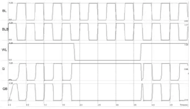
The schematic diagram of 6T SARM cell is as shown in figure 1a. During the read operation voltage is applied to the word line WL to turn ON the access transistors M5 and M6 and the memory cell discharges through either BL or BLB depending upon the stored data on nodes Q and QB. A sense amplifier converts the differential signal to a logic level output. During write operation voltage at WL is raised and BL’s are forced to either VDD, overpowering the contents of the memory cell.[3]
2.2 7T SR The sche connectio performe For read
Figure 1a. schem
RAM CELL ematic for 7T on between t ed through an operation bot
matic diagram for
Fig
T SRAM cell two inverters
extra NMOS h WL and R s
6T SRAM
gure 1c. Output w
l is as shown before write S transistor N5 signals are tur
waveform for WR
n in figure 2a e operations. 5 and cell only rned ON, whil
Fi
RITE operation in
a. This desig The feedbac y depends on le N5 is kept O
gure 1b. layout fo
n 6T
gn depends on ck connection n BL_bar to pe
ON. [2]
or 6T SRAM
n cutting the n and disconn erform write o
feedback nection is
operation.
2.3 8T SR The sche conventio sensing d word line are effect
Figur
RAM CELL ematic for 8T onal 6T SRAM data through a e is used exclu tively elimina
re 2a. 7T SRAM
Fig
T SRAM cel M cell. The r a separate read
usively for wr ated.
cell
gure 2c. Output w
l is as show read operation d stack contro rite operations
waveform for WR
wn in figure 3 n can be entir olled by a sep s. With this ar
Figure 2b
RITE operation in
3a. Here two ely decoupled arate read wo rrangements c
. layout for 7T S
n 7T
transistors r d from write o ord lines (RW
cell disturbs d SRAM cell
read stack is operation in 8 WL) [3]. The or during a read o
added to 8T cell by riginal 6T operations
2.4 9T SR The sche SRAM c by an wr is compo are contr
Figur
RAM CELL ematic of 9TS
ell composed rite signal WL osed of bit line
rolled by the
re 3a. 8T SRAM
Fig
RAM cell is a of M3, M4, M L. Data is store
e access trans data store in
M cell
gure 3c. Output w
as shown in fi M5, M6, M1 a ed within upp sistors M7 and n the cell. M9
waveform for WR
figure 4a . The and M2. Two per memory su d M8 and the 9 is controlled
Figure 3b. La
RITE operation in
e upper sub-ci Write access ub-circuit. The
read access tr d by a separa
ayout for 8T SRA
n 8T
ircuit of 9T ce transistors M5 e lower sub-ci ransistor M9. ate read signa
AM
ell is a conven 5and M6 are c ircuit of 9T SR
Transistors M al RD. 9T SR
ntional 6T controlled RAM cell M7and M8 RAM cell
2.5 10T S The sche access tr implemen pre-charg advantag write por
Fig
SRAM CELL ematic for 10T ransistors M2
nt a buffer use ged to prior to ge of separatin
rts.
gure 4a. 9T SRAM
Fig
L
T SRAM cell 2, M5 (transi ed for reading o read access ng read and wr
M cell
gure 4c. Output w
is as shown in istors from w g. Read access s. The word li rite word line
waveform for WR
n figure 5a. W write bit lines s is single end
ine for read a es is that a me
Figure 4
RITE operation in
Write access to s BL and BL
ed and occurs also is distinc mory using th
b. Layout for 9T
n 9T
o the bit cell o LB) . transist s on a separate ct from the wr his bit cell can
SRAM cell
occurs through tors M7 thro e bit line RBL rite word line n have distinct
h the write ough M10 L, which is
e [3]. One t read and
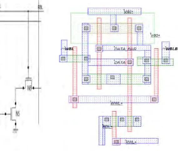
All the la environm analysis o 9T SRAM
Fig
ayouts have b ment all the lay
of the layouts M Cell at 12
gure 5a. 10T SRA
Fig
een simulated youts has been
stated above 20nm technolo
AM cell
gure 5c. Output w
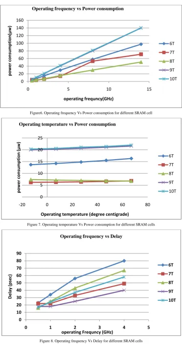
3. Simulat d using Microw
n simulated o at 120nm tech ogy shows al
waveform for WR
ion results an wind tool at 1
n the same in hnology. The lways best pe
Figure
ITE operation in
nd Analysis 120 nm techn nput patterns. F
simulation re erformance fo
e 5b. Layout for
10T
nology. To ma Figure 6-Figu esults reveal th or the range o
10T SRAM
ake the impart ure9 shows com
hat 8T SRAM of power con
tial testing mparative M Cell and sumption,
Figure6. Operating frequency Vs Power consumption for different SRAM cell
Figure 7. Operating temperature Vs Power consumption for different SRAM cells 0
20 40 60 80 100 120 140 160
0 5 10 15
power
consumption
(µw)
operating frequncy(GHz)
Operating frequency vs Power consumption
6T
7T
8T
9T
10T
0 5 10 15 20 25
‐20 0 20 40 60 80
power
consumption
(µw)
Operating temperature (degree centigrade)
Operating temperature vs Power consumption
6T
7T
8T
9T
10T
40 50 60 70 80 90
Delay
(psec)
Operating frequency vs Delay
6T
7T
8T
9T
Figure9. Operating temperature Vs Delay for different SRAM cells
4. Observations
The following are the observations for power and delay of different SRAM cells at room temperature with the operating frequency of 2GHz.
SRAM cells Power (µwatts) Delay (psec)
6T 14.808 56
7T 6.419 33
8T 7.004 39
9T 20.640 25
10T 20.923 37
Conclusion
The most efficient technique to reduce the power dissipation is the reduction of the supply voltage. The power dissipation reduction in SRAMs is not only due to power supply voltage reduction, but also to operating frequency and temperature. All the above figures depicts that 8T SRAM cell at 120nm technology and 9T SRAM cell at 120nm technology shows better performance for the range of frequency and temperature among all the other design approaches for SRAM cell. This paper tries to find out an efficient SRAM memory cell in both the aspects power consumption and speed.
References:
[1] Leland chang, Robert K. Montoye, Yutaka Nakamura, Kevin A.Batson, Richard J. Eickemeyer, Robert H Dennard, Wilfried Haensch
and Damir jamsek, “An 8T-SRAM For Variability Tolerence And Low Voltage Operation in High Performance caches”, IEEE Journal of solid state circuits , vol43, no.4, April 2008.
[2] Ramey E. Aly and Magdy A. Bayoumi, “Low Power Cache Design using 7T SRAM Cell”, IEEE Transactions on circuit systems-2;
EXPRESS BRIEFS, vol. 54, no.4, April 2007.
[3] Sapna Singh, Neha Arora, Meenakshi Suthar and Neha gupta, “Performance Evaluation of Different SRAM Cell Structures at
Different technologies”, International journal VLSI design &communication systems(VLSICS), vol.3, no.1, February 2012.
[4] Zhiyu Liu, Volkan Kursun, “ Characterization of a novel nine transistor SRAM cell”, IEEE Transactions on Very Large Scale
Integration Systems,vol.46, Issue 4,April 2008.pp-488-492. 0
10 20 30 40 50 60 70
‐20 0 20 40 60 80
delay
(psec)
operating temprarture (degree centigrade)
Operating temprature vs Delay
6T
7T
8T
9T
10T