High Efficiency LED Drivers: A Review
Mrs. Vishakha Phatangare
Research Scholar, Department of EEE, Karpagam Academy of Higher Education, Coimbatore, Tamil Nadu, India
Abstract — Recently various soft switching techniques
have been developed for various DC-DC based LED drivers. Typical driver circuits in the market have efficiency between 80% - 95% with majority having efficiency between 80% - 90%. Various topologies and strategies are available to obtain the best performance. A comparison and discussion of different buck and floating buck topologies used as driver in LED lighting application are presented in this paper.
Keywords—Adaptive timing difference compensation (ATDC), Hysteresis current control (HCC), Peak current control (PCC) .
I. INTRODUCTION
Now a day’s use of LEDs has increased across the world. LEDs offer significantly better luminous efficacy, provide long life span and environment friendly properties. Due to low power dissipation, there is considerable electricity saving. Therefore, LEDs are very promising light source and are widely used in many applications such as indoor lighting, display, automotive lighting, back lighting and street lights. For such applications, It is preferred to connect LEDS in Series or Parallel (multiple LED strings) to get more brightness. The brightness of LED is proportional to its conduction current. To regulate LED current is very challenging task .To ensure proper operation special drivers( DC-Dc converters) are required. It’s true that LEDs still do not dominate the lighting market over traditional lighting sources, because LED systems are less cost effective. Therefore bringing down the cost of LED system is a challenge in designing LED driver. Generally such drivers can be realized using buck or floating buck topologies.
Peak current control (PCC)[1],[2] and hysteresis current control (HCC)[2]-[4] are two basic schemes to regulate the average LED current. This control scheme is used in buck and floating buck –based LED driver.
Problems in Peak current control (PCC) and hysteresis current control (HCC):
1) Peak current control (PCC) : When D> 0.5 , PCC suffers from sub harmonics oscillations .To avoid this slope compensation is applied. But due to slope compensation current accuracy degrades. [5]-[8]
2) Hysteresis current control (HCC): To get current accuracy, hysteresis current control (HCC) )[2]-[4] is used . In this scheme current sensing resistor is used in
series with inductor, so that large current flowing during entire switching period which will give higher conduction loss.
3) Adaptive Off –Time Control: Small conduction losses than HCC and better current accuracy than PCC. But require long calibration time and settling time for current regulation and hence limit the current accuracy if switching frequency is high[9],[10].
4) Adaptive timing difference compensation (ATDC): Provides high current accuracy, fast settling time and high converter frequency.[11]
In recent research new drivers are developed to overcome above problems.
II. PI COMPENSATOR DESIGN OF
DUTY-CYCLE CONTROLLED BUCK LED DRIVER[12]
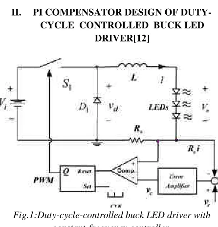
Fig.1:Duty-cycle-controlled buck LED driver with constant-frequency controller.
Fig 1 shows duty-cycle-controlled buck LED driver with constant-frequency controller. PI compensator is used as an example of the error amplifier in this scheme as shown in fig 2.
Fig.2: PI error amplifier circuit
Fig.3: PI gain curve for the critically damped response.
The duty-cycle controlled buck LED driver is always unstable for Kp = 0. The stable integral gain range is very wide for a given P gain. In practical design, it is desirable that the transient response of the inductor current should be critically damped or slightly overdamped to avoid an oscillatory LED current( fig 3). Based on this concept, the PI gains can be determined at the maximum D in the range of operating region. Therefore, for a good transient response, the P gain kp slightly greater than or equal to
can be selected. Selecting the PI gains of the error amplifier according to this practical design equation is very easy and useful for stability and current accuracy point of view.
Fig.4:Structure of the dimmable ATDC LED driver
III. ADAPTIVE TIMING DIFFERENCE
COMPENSATION (ATDC)[11]
A new control scheme: adaptive timing difference compensation (ATDC) is shown in fig 4. to regulate Iavg for achieving: 1) high current accuracy; 2) fast
settling time during dimming control; and 3)high converter operation frequency.
Fig.5:Timing diagram of the Inductor/LED current in the proposed ATDC scheme.
The average LED current in the floating-buck converter is given as
Where I peak and ΔIL are peak inductor/LED current and inductor/LED current ripple, respectively. L is the inductance used in the power stage, and Ton and Toff are on-time and off-time of power nMOS MN in Fig. 4. From 1), if the input voltage of the driver changes or the number of output LEDs (thus output voltage) varies, then the inductor current Ripple ΔIL and thus I avg will be changed correspondingly, compromising the accuracy of the LED current. In order to maintain Iavg to a constant value for high current accuracy under variations of VIN and VOUT, Toff should be adjusted adaptively. Fig. 5 illustrates the proposed ATDC scheme to adjust Toff based on the timing diagram of the LED current. In Fig.5. TH and TL are time durations that ILED is higher and lower than the desired average current Iavg.OPT. respectively. In order to achieve Iavg = Iavg.OPT. it needs to ensure TL = TH. The proposed ATDC scheme will thus adjust Toff(n) adaptively according to the following equation as
Toff(n) = Toff(n-1) – G . (TL(n) – TH(n))
such that the off-time of power nMOS MN settles to a constant value and Iavg reaches Iavg.OPT. In case of TL(in) > TH(n), Toff(n) will be decreased based on (2) and eventually results in TL = TH. It should be noted that the proposed ATDC scheme is realized by a digital controller with a typical clock frequency (dCLK) of 160 MHz. Since the maximum switching frequency of the proposed LED driver is 1 MHz, the digital controller is thus sufficiently fast to enable off-time calculation in every switching cycle (1 µs) of the converter under variations of input and output voltages. Additionally, the proposed ATDC scheme only needs a single low-side current sensor to detect the peak inductor / LED current for determining TH - TL.
Settling Time and Stability Considerations :
Fig.6 shows the settling behavior of the LED current once the PWM dimming signal is triggered. Fast settling time TSettle is important not only to enable high dimming frequency but also to minimize the current difference between Iavg.s1 (or Iavg.s2) and Iavg.OPT during the transient, where Iavg.s1 = shaded area A1/TSettle < Iavg.OPT and Iavg.s2 = shaded area A2/TSettle > Iavg.OPT. Hence, fast settling time is important to improve the LED current accuracy especially under low dimming duty ratios of the short dimming period that give rise to larger current difference between Iavg.s1 (or Iavg.s2) and Iavg.OPT.
To achieve fast settling time, the value of G in (2) should be maximized. However, if G is too large, the ATDC driver could suffer from the sub harmonic oscillation due to too much increase or decrease in the next-cycle Toff. On the other hand if the value of G is too small, it could take too long for the ATDC scheme to stabilize the average LED current to Iavg.OPT under perturbations of input or output voltages or sudden turning on the dimming signal, although the LED driver will be unconditionally stable. Therefore, the gain decision comparator (COMP3) is introduced in the proposed LED driver to simultaneously ensure stability and achieve the fast settling time under a wide range of input voltages and different number of output LEDs
Fig.6: Current offsets due to settling once dimming is triggered
The proposed ATDC control scheme enables the driver to achieve fast settling time and high current accuracy over a wide range of input voltages and output LED loads. The
power efficiency of the HV LED driver benefits from having no sensing resistor in the power stage and using the on-chip synchronous rectification via the high-speed low-power synchronous gate driver with pseudo-digital level shifters. The proposed LED driver can also operate at a high switching frequency due to high processing speed of the digital controller as well as high-speed low-power current sensor and synchronous gate driver.
IV. MULTICHANNEL LED DRIVERS[13]
Variety of multichannel LED drivers are proposed previously :
Multichannel LED driver based on LLC resonant converter[14]: In this scheme transformer modules are in series on primary side and each transformer module drives two LED strings. On the secondary side, full bridge structure is adopted and currents of two LED strings are balanced by dc blocking capacitor. It is easy to achieve low dimming, but it is difficult to adopt the variation of LED number and string number without redesigning the power stage.[14]
Another LED driver proposed in [15] is voltage fed half bridge topology. It can drive multiple LED strings at the same time but difficult to adapt load variation.
LLC resonant converter proposed in [16] can adopt variation of string number, but difficult to adapt to the variation of LED number.
LLC based single stage scheme proposed in [17] and[18], the switching frequency of LLC converter is regulated when LED dims or load varies.
The high efficiency cannot be guaranteed with dimming and load variation because LLC does not always work at optimum point.
To solve above problems in multichannel LED driver, a new two stage driver is proposed as shown in Fig. 7. [13] In this scheme first stage is buck converter and MC3 CLL resonant converter is second stage.
It achieves good current balance among LED strings. It also maintains high efficiency over a wide load range and adapt to the load variation.
It achieves good current balance among LED strings. It also maintains high efficiency over a wide load range and adapt to the load variation. For second stage, only one CLL resonant tank is provided which consists of Cr, Lr1 and Lr2. In addition, transformer modules are in series on the primary side. Voltage doublers structure is adapted on the secondary side. One transformer can drive two LED strings at a time. The current of the two LED strings driven by the same transformer are balanced via blocking capacitor Cdc, which is series with secondary side winding of transformer. Whatever the voltage difference is, the current of these two LED strings will be identical. Even the number of LED per string is different, the current will be identical. The currents of multiple, LED string is also identical. The transformer module can be added and removed according to the variation of the LED string number. The current of one LED strings is sensed for feedback control to tune the duty cycle of buck converter. Vbus which is input voltage of MC3 CLL, is adjusted according to dimming requirement. Even number of LED strings or the number of LEDs per string changes, Vbus will be adjusted as well. MC3CLL resonant converter is unregulated. It is always working at series resonant frequency to maintain high efficiency over wide load range.
In buck converter Sic diode is applied as freewheeling diode to reduce turn on loss of high side switch. The high side switch is optimized according to the tradeoffs between conduction loss and switching loss. Buck converter is working in continuous conduction mode over wide load range.The junction capacitor of secondary side rectifier influence the ZVS achievement of primary side switches. Thus, this two stage LED driver is good candidate for good current balance and high efficiency.
V. NEW HIGH EFFICIENCY LED DRIVER
CIRCUIT[22]
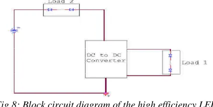
The new high efficiency power supply in its simplest form is shown in Fig. 8. It consists of a voltage source which supplies power to an LED string which is split into two sections. A first LED string (load 1) is driven by a conventional dc-to-dc converter, whereas a second LED string (load 2) is placed in series with the incoming dc supply current. The dc-to-dc converter operates to provide a voltage in opposition to the voltage source such that the voltage across and current through load 2 is regulated simultaneously. The dc-to-dc converter also supplies and controls the current in load 1.The simplest dc-to-dc converter and the one that will be used in this paper is the buck converter.
Fig. 9 shows the complete new high efficiency power supply with the dc-to-dc converter replaced with the circuitry for the buck converter, where VO1 is the voltage
across load 1, Vs is the supply voltage, and VO2 is the voltage across load 2.Load 2 is a string of LEDs consisting of D2a and D2b connected in series. Load 1 is also now represented as a string of LEDs consisting of D1a and D1b connected in series. The output of the buck converter is controlled by the MOSFET, M1, which has a duty ratio controlled by pulse width modulation (PWM). If the current, in the inductor does not drop to zero when the power switch is OFF, the inductor current is said to be continuous. In order to get continuous current, the inductance must be greater than . Lmin = T R(1 − D)/2
Fig.8: Block circuit diagram of the high efficiency LED power supply.Load 1 and load 2 are LED strings and Vs
is the voltage supply.
where D is the duty ratio of the PWM, Lmin is the minimum inductance of L1 in Fig. 9, T is the switching period of the PWM, and R is the total resistance of the LEDs when in series [19]. The minimum inductance was found at minimum duty cycle and maximum load based on a chosen switching frequency .Assuming the continuous inductor current, the voltage across load 1, VO1, is given by
VO1/(Vs − VO2)= D
When the current through the inductor is continuous, the relationship between the supply current flowing through load 2, IO2, and the current in load 1, IO1, is given by IO1/IO2= 1/D
Load 1 is an LED string so there is little variation in the forward voltage as the current increases and so VO1 can be considered to be approximately constant [20], [21]. If the duty ratio is varied inversely with Vs − VO2 a relatively constant voltage will be maintained across load 2 and the current in load 2 will also be constant. This circuit provides controlled current in load 2 by providing a compensation voltage at the terminals which automatically changes to oppose any variation in supply voltage. The major benefit of this circuit for the control of LEDs is its high efficiency. The input power to the whole circuit is
Pinput = IO2Vs .
There are no losses in the delivery of the power to load 2, so the useful output power of the whole circuit is Poutput = IO2VO2 + ηIO2(Vs − VO2)
The efficiency of the whole circuit will always be higher than the buck converter alone [21].
A further advantage of this design is that since a significant percentage of the supply voltage is dropped across load 2 the voltage ratings of the electronic components in the buck converter can be lower, giving lower losses, and further increasing the system efficiency.
.
Fig.9: New high efficiency circuit used for the simulations with a standard buck circuit used as the dc-to-dc
converter.
VI. CONCLUSION
Different buck and floating buck topologies have been discussed in this paper. The solution chosen by the designer depends on particular design constraints. High efficiency of buck converter can be achieved by different schemes as follows :
Duty cycle controlled Buck LED driver is always unstable for kp = 0. In scheme[12],Selecting PI gains of error amplifier according to the equation mentioned in analysis very easy and useful for stability and current accuracy point of view.
There is no sensing resistor used in scheme(11), hence, no conduction losses and high efficiency is achieved. It also achieves fast settling time and high current accuracy over wide range of input voltage and output LED loads. Scheme [13] uses two stage structure i.e. Buck converter and MC3 CLL resonant converter. Buck converter uses Sic diode as freewheeling. Due to this, turn on losses of high side switch reduces and soft switching can be achieved. MC3 CLL always works at resonant frequency and maintains high efficiency over wide load range. Simplicity is the main feature of the scheme [22]. The basic Buck converter is slightly modified to get higher system efficiency. It also reduces the rating of the component used in Buck converter. So that losses are reduced and there is further improvement in efficiency. As system [22] is simple and having low cost, it is the most competitive solution amongst the other more advanced topologies .For wide load range and dimming application ,scheme [13] is preferred.
REFERENCES
[1] I. H. Oh, “An analysis of current accuracies in peak and hysteretic current controlled power LED drivers,” in Proc. IEEE Appl. Power Electron.Conf., pp. 572–577. Feb. 2008
[2] Supertex Inc., “HV9910B: Universal high brightness LED driver,” 2005
[3] Diodes Inc., “ZXLD 1350: 30V350mALED driverwithAEC-Q100,”2011.
[4] On Semiconductors Inc., “CAT 4201: 350 mA high-efficiency stepdown LED driver,” Datasheet Rev. 8, May 2011.
[5] C. F. Lee and P. K. T. Mok, “A monolithic current-mode CMOS DC-DC converter with on-chip current sensing technique,” IEEE J.Solid-State Circuits, vol. 39, no. 1, pp. 3–14, Jan. 2004.
[6] H. Pooya Forghani-zadeh and G. A. Rincon-Mora, “An accurate, continuous,and lossless self-learning CMOS current-sensing scheme for inductor-based DC-DC converters,” IEEE J. Solid State Circuits, vol.42, no. 3, pp. 665–679, Mar. 2007.
[7] M. Du and H. Lee, “An integrated speed- and accuracy-enhanced CMOS current sensor with dynamically-biased shunt feedback for current-mode buck regulators,” IEEE Trans. Circuits Syst. I, Reg.Papers, vol. 57, no. 10, pp. 2804–2814, Oct. 2010.
[8] M.Du, H. Lee, and J. Liu, “A5-MHz 91%peak-power-efficiency buck regulator with auto-selectable peak- and valley-current control,” IEEE J. Solid State Circuits, vol. 46, no. 8, pp. 1928–1939, Aug. 2011.
[9] C. H. Liu, C. Y. Hsieh, Y. C. Tai, T. J. Tai, and K. H. Chen, “SAR-controlled adaptive off-time technique without sensing resistor for achieving high efficiency and accuracy LED lighting system,” IEEE Trans. Circuits Syst. I, Reg. Papers, vol. 57, no. 6, pp. 1384–1394,Jun. 2010.
[10] On Semiconductors Inc., “NCL30160: 1.0 A constant-current buck regulator for driving high power LEDs,” 2012.
[11] Dongkyung Park, Zhidong Liu and Hoi Lee,” A 40 V 10 W 93%-Efficiency Current-Accuracy- Enhanced Dimmable LED Driver With Adaptive Timing Difference Compensation for Solid-State Lighting Applications”, IEEE Journal Of Solid-State Circuits, Vol. 49, No. 8,Pp1848-1859,August 2014 [12] Marn-Go Kim” Proportional-Integral (PI)
[13] Xuebing Chen, Daocheng Huang, Qiang Li, and Fred C. Lee, ”Multichannel Led Driver With Cll Resonant Converter” Ieee Journal Of Emerging And Selected Topics In Power Electronics, Vol. 3, No.3,Pp589-597, September 2015
[14] S.-S. Hong, S.-H. Lee, S.-H. Cho, C.-W. Roh, and S.-K. Han,“A new cost-effective current-balancing multi-channel LED driver for a large screen LCD backlight units,” J. Power Electron., vol. 10, no. 4,pp. 351–356, Jul. 2010.
[15] J. Zhang, L. Xu, X. Wu, and Z. Qian, “A precise passive current balancing method for multioutput LED drivers,” IEEE Trans. Power Electron., vol. 26, no. 8, pp. 2149–2159, Aug. 2011.
[16] S. Choi and T. Kim, “Symmetric current-balancing circuit for LED backlight with dimming,” IEEE Trans. Ind. Electron., vol. 59, no. 4,pp. 1698–1707, Apr. 2012.
[17] J. Zhang, J. Wang, and X. Wu, “A capacitor-isolated LED driver with inherent current balance capability,” IEEE Trans. Ind. Electron., vol. 59,no. 4, pp. 1708–1716, Apr. 2012.
[18] H. Wu, S. Ji, F. C. Lee, and X. Wu, “Multi-channel constant current (MC3) LLC resonant LED driver,” in Proc. IEEE Energy Convers.Congr. Expo, pp. 2568–2575. Sep. 2011.
[19] M. Fisher, Power Electronics. Austin, TX, USA: Thomson Information Publishing Group, 1991, p. 294.
[20] C. Pollock and H. Pollock, “High efficiency LED power supply,”U.S. Patent 8 853 953 B2, Oct. 7, 2014.
[21] C. Pollock and H. Pollock, “LED power supply,” U.S. Patent 8 890 422,Jan. 24, 2013.