
University of Pennsylvania
ScholarlyCommons
Publicly Accessible Penn Dissertations
2018
Choose-Your-Own Adventure: A Lightweight,
High-Performance Approach To Defect And
Variation Mitigation In Reconfigurable Logic
Raphael Yoram Rubin
University of Pennsylvania, [email protected]
Follow this and additional works at:https://repository.upenn.edu/edissertations
Part of theComputer Engineering Commons, and theComputer Sciences Commons
This paper is posted at ScholarlyCommons.https://repository.upenn.edu/edissertations/3178
Recommended Citation
Rubin, Raphael Yoram, "Choose-Your-Own Adventure: A Lightweight, High-Performance Approach To Defect And Variation Mitigation In Reconfigurable Logic" (2018).Publicly Accessible Penn Dissertations. 3178.
Choose-Your-Own Adventure: A Lightweight, High-Performance
Approach To Defect And Variation Mitigation In Reconfigurable Logic
Abstract
For field-programmable gate arrays (FPGAs), fine-grained pre-computed alternative configurations, combined with simple test-based selection, produce limited per-chip specialization to counter yield loss, increased delay, and increased energy costs that come from fabrication defects and variation. This lightweight approach achieves much of the benefit of knowledge-based full specialization while reducing to practical, palatable levels the computational, testing, and load-time costs that obstruct the application of the knowledge-based approach. In practice this may more than double the power-limited computational capabilities of dies fabricated with 22nm technologies.
Contributions of this work:
• Choose-Your-own-Adventure (CYA), a novel, lightweight, scalable methodology to achieve defect and variation mitigation
• Implementation of CYA, including preparatory components (generation of diverse alternative paths) and FPGA load-time components
• Detailed performance characterization of CYA
– Comparison to conventional loading and dynamic frequency and voltage scaling (DFVS)
– Limit studies to characterize the quality of the CYA implementation and identify potential areas for further optimization
Degree Type
Dissertation
Degree Name
Doctor of Philosophy (PhD)
Graduate Group
Computer and Information Science
First Advisor
André M. DeHon
Keywords
Subject Categories
CHOOSE-YOUR-OWN ADVENTURE:
A LIGHTWEIGHT, HIGH-PERFORMANCE APPROACH TO DEFECT AND VARIATION MITIGATION IN RECONFIGURABLE LOGIC
Raphael Yoram Rubin
A DISSERTATION
in
Computer and Information Science
Presented to the Faculties of the University of Pennsylvania in Partial Fulfillment of the Requirements for the Degree of Doctor of Philosophy
2018
Supervisor of Dissertation
Andr´e M. DeHon, Professor Electrical and Systems Engineering
Graduate Group Chairperson
Lyle Ungar, Professor Computer and Information Science
Dissertation Committee:
Jonathan M. Smith, Pompa Professor of Engineering and Applied Science Boon Thau Loo, Professor of Computer and Information Science Joseph Devietti, Assistant Professor of Computer and Information Science
CHOOSE-YOUR-OWN ADVENTURE:
A LIGHTWEIGHT, HIGH-PERFORMANCE APPROACH TO DEFECT AND VARIATION MITIGATION IN RECONFIGURABLE LOGIC
COPYRIGHT
Raphael Yoram Rubin
2018
This work is licensed under the Creative Commons Attribution-NonCommerical-ShareAlike 4.0 International
(CC BY-NC-SA 4.0) License. To view a copy of this license, visit:
Acknowledgements
People
I’d like to thank my advisor, Andr´e DeHon, and my committee chair, Jonathan M. Smith, for seemingly unlimited patience and support. I am also grateful to the rest of my committee, Boon Thau Loo, Joe Devietti, and Steve Trimberger for their feedback and approval.
My labmate, Ben Gojman, has been my unwavering comrade in arms during our Ph.D. studies, an excellent research collaborator and aesthetic advisor, and a caring friend. Nikil Mehta and Hans Giesen have also been key research contributors and valuable friends.
My parents, Alice Palokoff and David Rubin, have been waiting for far too long to see this dissertation done. I hope the results vindicate their many years of anticipation and encouragement.
Funding
In addition to the amazing people above, this research was also supported by the following funding sources:
• NSF grants CCF-0403674, CCF-0726602, CCF-0904577, and CNS-1406225
• DARPA grant HR0011-13-C-0005
• ONR grant N00014-15-1-2006
• Toshiba Corporation
• the University of Pennsylvania School of Engineering and Applied Science
ABSTRACT
CHOOSE-YOUR-OWN ADVENTURE:
A LIGHTWEIGHT, HIGH-PERFORMANCE APPROACH TO DEFECT AND VARIATION MITIGATION IN RECONFIGURABLE LOGIC
Raphael Yoram Rubin
Andr´e M. DeHon
For field-programmable gate arrays (FPGAs), fine-grained pre-computed alternative configurations, combined with simple test-based selection, produce limited per-chip specialization to counter yield loss, increased delay, and increased energy costs that come from fabrication defects and variation. This lightweight approach achieves much of the benefit of knowledge-based full specialization while reducing to practical, palat-able levels the computational, testing, and load-time costs that obstruct the appli-cation of the knowledge-based approach. In practice this may more than double the power-limited computational capabilities of dies fabricated with 22nm technologies.
Contributions of this work:
• Choose-Your-own-Adventure (CYA), a novel, lightweight, scalable methodology to achieve defect and variation mitigation
• Implementation of CYA, including preparatory components (generation of di-verse alternative paths) and FPGA load-time components
• Detailed performance characterization of CYA
– Comparison to conventional loading and dynamic frequency and voltage
scaling (DFVS)
– Limit studies to characterize the quality of the CYA implementation and
Contents
Acknowledgements iv
Abstract vi
Contents vii
List of Tables xii
List of Figures xiv
List of Algorithms xvii
1 Introduction 1
1.1 Hypothesis . . . 1
1.2 The Problem . . . 1
1.3 Previous Strategies . . . 3
1.3.1 Component-Specific Mapping (CSM) . . . 6
1.4 CYA: Path-Multiplicity Based CSM . . . 10
1.5 Results . . . 13
1.6 Pertinent Publications . . . 16
1.7 Who Did What . . . 18
2 Setting 20
2.1 International Technology Roadmap for Semiconductors . . . 20
2.2 Transistor Fundamentals . . . 21
2.3 What Has Changed? . . . 25
2.4 Summary . . . 27
3 Current Solutions 28 3.1 Chapter Organization . . . 30
3.2 Techniques That Address Variations Only . . . 30
3.2.1 Statistical Static Timing Analysis (SSTA) . . . 30
3.2.2 Body Biasing . . . 31
3.2.3 Clock Phase Skewing and Slack Stealing . . . 31
3.3 Techniques That Address Low Defect Rates . . . 32
3.3.1 Multiple Bitstreams . . . 32
3.3.2 EasyPath™ . . . 33
3.4 Techniques That Address High Defect Rates . . . 33
3.4.1 Modular Redundancy . . . 33
3.4.2 Hardware-Sparing In-Factory Repair . . . 34
3.4.3 Avoiding Faults . . . 35
4 CYA 37 4.1 Inspiration . . . 38
4.1.1 Illustrative Example . . . 38
4.2 CYA Components . . . 40
4.2.1 CYA Bitstream . . . 41
4.2.2 Routing . . . 42
4.2.4 Bitstream Loader . . . 44
4.3 Alternative Diversity . . . 47
4.3.1 Problems with Resource-Cost Alternatives Generation . . . . 47
4.4 Foundational Experiments . . . 53
4.4.1 Experimental Framework . . . 54
4.4.2 Experimental Flow . . . 56
4.4.3 Experimental Architecture . . . 57
4.4.4 Experimental Design . . . 59
4.5 Initial Results . . . 60
4.5.1 Path-Cost Algorithm vs. Resource-Cost Algorithm . . . 62
4.5.2 C-Box Population . . . 62
4.5.3 Additional Tracks . . . 62
4.5.4 Impact on Circuit Delay . . . 68
4.5.5 Impact of Switch and Wire Defects . . . 71
4.5.6 Summary . . . 73
4.6 Bitstream Impact . . . 73
4.6.1 Bitstream Size . . . 75
4.6.2 Bitstream Load Time . . . 78
4.6.3 Updated Bitstream Tables . . . 81
4.7 Repair of Different Resource Types . . . 85
4.7.1 The Fabric and the Tile . . . 85
4.7.2 Channel Wires . . . 85
4.7.3 Input C-Boxes . . . 88
4.7.4 S-Boxes and Output C-Boxes . . . 90
4.7.5 CLB Pins . . . 90
4.7.7 All Resource Types . . . 91
5 Failure Modes and Defect Models 104 5.1 Functional Faults . . . 105
5.1.1 Incorrect Inversions . . . 105
5.1.2 Outputs That Are Not Functions of the Source . . . 106
5.1.3 Functions With Unintended Inputs . . . 106
5.1.4 Example Test Circuit . . . 108
5.2 Delay Faults . . . 109
5.2.1 Delay Budgeting . . . 110
5.2.2 Test Circuit and Procedure . . . 113
5.2.3 Single Frequency Delay Results . . . 116
6 Delay and Energy Optimization with CYA 121 6.1 Delay Optimization . . . 121
6.2 Energy Optimization . . . 125
6.2.1 Energy Impacts of Voltage Reduction and Variations . . . 125
6.2.2 Experiments . . . 133
7 Limit Studies 142 7.1 Pathfinder Negotiated Alternative Selection . . . 143
7.2 Pathfinder Knowledge-Based Repair . . . 149
7.3 Full-Knowledge Routing . . . 155
7.4 CYA and the Costs and Benefits of Component-Specific Mapping . . 160
8 Conclusions and Future Prospects 169
A Topological Systematic Error 173
A.1 Resource Quantity . . . 175 A.2 Resource Properties . . . 176
B Architecture Files 186
B.1 4x4 fcin 1.00 fcout 1.00.arch . . . 186 B.2 4x4 fcin 0.50 fcout 0.25.arch . . . 189 B.3 One alt guaranteed seg len 4.xml . . . 192
Acronyms 200
List of Tables
2.1 ITRS scaling and process variation projections . . . 26
4.1 Full-yield 95% confidence interval vs. # of chips . . . 60
4.2 CYA yield improvement for Toronto 20 benchmarks (VPR 4.3) . . . . 74
4.3 Bitstream table parameters . . . 75
4.4 CYA bitstream sizes for Toronto 20 benchmarks (VPR 4.3) . . . 76
4.5 CYA bitstream load times for Toronto 20 benchmarks (VPR 4.3) . . 79
4.6 Toronto 20 benchmark parameters for VPR 5 . . . 82
4.7 CYA bitstream sizes for Toronto 20 benchmarks (VPR 5) . . . 83
4.8 CYA bitstream load times for Toronto 20 benchmarks (VPR 5) . . . 84
4.9 Resource area data (22nm technology) . . . 92
4.10 Distribution of max CYA-repairable defect density (Toronto 20) . . . 100 4.11 CYA yield improvement for Toronto 20 benchmarks (VPR 5) . . . 102
5.1 Variables for slack calculations . . . 112
6.6 DFVS and CYA energy savings vs. conventional loading (Toronto 20) 139 6.7 DFVS and CYA variation energy loss mitigation (Toronto 20) . . . . 140
7.1 Energy and voltage, Pathfinder alternative selection (Toronto 20) . . 148 7.2 Energy and voltage, Pathfinder knowledge repair (Toronto 20) . . . . 154 7.3 Energy and voltage, full-knowledge routing (Toronto 20) . . . 159 7.4 Median energy usage of CSM methods (Toronto 20) . . . 162 7.5 Median % of possible CSM energy savings obtained (Toronto 20) . . . 164
7.6 Median % of possible low-Vdd energy savings obtained (Toronto 20) . 166
7.7 Median % recovery of energy lost due to variations (Toronto 20) . . . 168
List of Figures
1.1 Defect repair on an FPGA using resource interchangeability . . . 6
1.2 Avoiding multiple defects with one repair path . . . 8
1.3 Repair flexibility via path multiplicity . . . 8
1.4 CYA CAD flow vs. conventional flow . . . 10
1.5 Yield improvement via CSM . . . 17
2.1 Cartoon resistor . . . 21
2.2 Basic structure of a MOSFET . . . 22
2.3 Operation of a planner MOSFET . . . 23
4.1 FPGA channel with base and reserved tracks . . . 38
4.2 CYA CAD flow (reprise) . . . 40
4.3 Path-Cost Algorithm motivating examples . . . 48
4.4 Paths tree generation . . . 49
4.5 Duplicate detection and new path addition using a paths tree . . . . 50
4.6 Buffered switch and wire segment model . . . 58
4.7 Yield benefits of CYA alternatives . . . 61
4.8 Resource-Cost/Path-Cost yield comparison . . . 63
4.9 Effects of C-Box population on yield . . . 64
4.11 Effects of reserved tracks on yield . . . 66
4.12 Effects of extra base tracks vs. reserved tracks . . . 67
4.13 Yield and delay preservation by CYA at high defect rates . . . 69
4.14 Effects of stuck-open switch and broken-wire defect types . . . 72
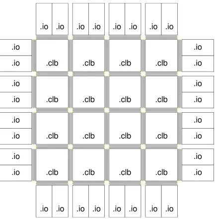
4.15 FPGA block diagram . . . 86
4.16 FPGA tile wiring diagram . . . 87
4.17 Bridge faults in staggered interconnect . . . 88
4.18 Directional single-driver segment wiring diagram . . . 89
4.19 Bi-directional multi-driver segment wiring diagram . . . 89
4.20 Yield impact of bridges vs. breaks . . . 93
4.21 Yield impact of CLB input buffer defects . . . 94
4.22 Yield impact of S-Box buffer defects . . . 95
4.23 Yield impact of CLB I/O pin wire breaks . . . 96
4.24 Yield impact of dead subblocks . . . 97
4.25 Combined yield impact of all defect types (per-resource defect model) 98 4.26 Combined yield impact of all defect types (per-area defect model) . . 99
4.27 Distribution of max CYA-repairable defect density (Toronto 20) . . . 101
4.28 CYA repair effectiveness for Toronto 20 benchmarks . . . 103
5.1 Transition and inversion fault testing circuit . . . 109
5.2 desslack histogram (nominal mapping) . . . 111
5.3 Harris delay self-test circuit . . . 114
5.4 Gojman delay measurement circuit and sample results . . . 115
5.5 CYA delay improvements at 0.8V in the presence of variations . . . . 118
5.6 CYA delay improvements at 0.7V in the presence of variations . . . . 119
6.1 Delay impact of voltage reduction in CYA . . . 123
6.2 Energy impact of voltage reduction in CYA . . . 124
6.3 Inverter delay distribution under variation . . . 129
6.4 Delay distribution vs. Vdd (Gojman measurements) . . . 130
6.5 Static/dynamic energy breakdown for a single multiplier . . . 131
6.6 Energy consumption vs. voltage for des(nominal chip) . . . 132
6.7 desenergy/operation vs. Vdd, all loading methods . . . 141
7.1 Delay yield, Pathfinder alternative selection and CYA (des) . . . 145
7.2 Energy yield, Pathfinder alternative selection and CYA (des) . . . 146
7.3 Energy vs. load time, Pathfinder alt. selection and CYA (Toronto 20) 147 7.4 Delay yield, adding Pathfinder knowledge repair (des) . . . 151
7.5 Energy yield, adding Pathfinder knowledge repair (des) . . . 152
7.6 Energy vs. load time, adding Pathfinder know. repair (Toronto 20) . . 153
7.7 Delay yield, adding full-knowledge routing (des) . . . 156
7.8 Energy yield, adding full-knowledge routing (des) . . . 157
7.9 Energy vs. load time, adding full-knowledge routing (Toronto 20) . . 158
7.10 % of possible CSM energy savings obtained (Toronto 20) . . . 163
7.11 % of possible low-Vdd energy savings obtained (Toronto 20) . . . 165
7.12 % recovery of energy lost due to variations (Toronto 20) . . . 167
A.1 Delay of stressed vs. relaxed locked static routes (Toronto 20) . . . . 177
A.2 Speed advantage of reserved resources for a single net . . . 179
A.3 Delay of unlocked vs. locked relaxed static routes (Toronto 20) . . . . 181
A.4 Delay of CYA vs. static mapping (Toronto 20) . . . 182
A.5 (CYA delay)/(static map delay) vs. voltage for Toronto 20 designs . . 183
List of Algorithms
4.1 Resource-Cost Algorithm for alternatives generation . . . 43
4.2 Bitstream Load Algorithm . . . 46
4.3 isUsable Function for Bitstream Load Algorithm . . . 47
4.4 Path-Cost Algorithm for alternatives generation . . . 51
4.5 PathCost.FindShortest Function for Path-Cost Algorithm . . . 52
Chapter 1
Introduction
1.1 Hypothesis
Pre-computed per-net alternatives provide a lightweight method to exploit the recon-figurability and redundancy of field-programmable gate arrays (FPGAs) to address fabrication defects and variations. The improvements to yield and energy efficiency can more than double power-limited performance of dies fabricated with 22nm tech-nologies.
1.2 The Problem
size-scaling. However, Moore’s Law scaling has now driven component sizes down to near-atomic scales, where detailed control over produced structures becomes increas-ingly difficult, if not impossible. Operating voltages must be raised and clocks must be slowed to compensate for the resulting variations, preventing the voltage from scal-ing with field-effect transistor (FET) feature size. Consequently, Dennard scalscal-ing has ended — energy-efficiency improvements no longer match the pace of transistor area scaling. We can no longer operate as many transistors as we can fabricate in a given area. This scaling mismatch is expected to worsen with continued scaling, leading to a steady increase in the fraction of each die which must remain inactive to meet strict power budgets. This trend/problem is commonly termed “Dark Silicon” [20].
Mehta [61] (elaborated in Mehta [59]) demonstrates that component-specific map-ping (CSM) can be used to improve operational energy efficiency for FPGAs. A com-plementary project, by Gojman [26], demonstrates how to perform the detailed delay characterization of each chip required for knowledge-based CSM. This represents a significant advance beyond Culbertson’s [14] defect-only characterization (detection of lost signals, as opposed to the slowing of signals caused by variations). However, Gojman’s characterization methodology requires days or even weeks of analysis for a single chip, and utilizing these measurements requires redoing stages of the design compilation for each individual chip. The run times of current place-and-route tools are already considered overly burdensome, often taking hours or even days. Multi-plying that cost by the number of deployments, while at the same time adding sub-stantial per-chip characterization costs, is more than sufficient to prevent widespread adoption.
coarse-grained as-needed testing. This approach avoids the per-chip computer-aided de-sign (CAD), complete characterization, and data management challenges that plague Mehta’s knowledge-based approach. Despite having much less chip-specific informa-tion, CYA achieves on average 52% of the energy savings of knowledge-based CSM that are specifically attributable to the customization of the mapping (Table 7.5). In addition, both techniques inherently incorporate a form of dynamic frequency and voltage scaling (DFVS) (see Section 1.3). Counting the effects of DFVS, CYA achieves on average 83% of the total energy savings of knowledge-based CSM relative to con-ventional loading practices (Table 7.6). This dissertation describes the details of the CYA methodology and its implementation, and presents experiments demonstrating its capabilities, sensitivities, and limitations.
1.3 Previous Strategies for Mitigating
Post-Fabri-cation Defects and Variations
Some post-fabrication strategies use low-level physical approaches to effectively re-move defects and reduce variations. Body biasing [80, 63, 48] is one such technique. Body biasing divides the chip into control regions and shifts the threshold voltage
in each region in order to reverse variation-induced Vth shifts. This works well when
Vth shifts are spatially correlated or uniform across an entire die. However, with
ran-dom variations (an increasing concern, see [43]), neighboring transistors may vary in
opposite directions from nominal Vth. In such a case, applying a single correction
address random variations. For a more detailed analysis see Section 3.2.2.
Architectural sparing (including extra resources to replace defective ones), such as the row and column sparing used by Altera [13, 57, 47] and the segment sparing described by Yu [95], is another relatively low-level corrective approach. However, both the extra resources and their supporting infrastructure add area and delay, which also increases energy costs. Moreover, in light of variations, it is difficult to determine a priori which resources to discard or remap when the specific operational voltage is not known. This determination can be made at load-time, but at this point the sparing approach takes on the character of CSM, becoming more of an architectural optimization for that purpose than a distinct solution.
As variations increase, it becomes more important not only to correct or mitigate variations, but also to more precisely quantify what correction or mitigation even means. Specifically, we want to be able to say that, using a given correction protocol, a certain class of designs can be expected to operate reliably on chips with a certain level of variations, within certain voltage, clock speed, and other operating parameter ranges, for the full desired lifetime of the device. I refer to the process of establishing these parameter ranges as “margining”.
Acquiring more detailed knowledge about the properties of each individual chip often enables one to certify some chips for use with more demanding operational pa-rameters (i.e., tighter margins). For example, speed/power binning is the practice of testing chips at a few different clock speeds and voltages to determine the rough performance characteristics of each chip. The chips that are reliable at higher fre-quencies or lower voltages are offered at a premium commensurate with the extra utility to customers, rather than limiting all chips to the safe settings of the worst of the bunch.
combination, dynamic frequency and voltage scaling (DFVS), take this knowledge-based customization a step further, adjusting the supply voltage, clock speed, or both to save power while maintaining the requirements of a specific application or workload. For FPGAs, DVS/DFS often refer to the determination of an appropriate supply level/clock speed for a specific design on a given chip, rather than continuing to adjust these parameters during operation to match current workloads. DVS/DFS can only optimize the efficiency/speed at which a pre-determined mapping operates on any given chip, and so their effectiveness is limited by the worst of that chip’s resources (transistors, wires, etc.) used by the given mapping. This limitation can be addressed with the use of CSM to replace bad resources with better resources, enabling dynamic scaling to achieve lower voltages/higher clock speeds.
At this point in the process, we have accepted the demise of the perfect-chip assumption. The next step now becomes resilient design: creating circuits that will operate correctly on partially defective and otherwise variable hardware. The classic modular redundancy approach [65, 10, 2, 67] provides solutions to high rates of defects, but comes with a high cost. The minimum implementation triplicates (in special cases duplicates) a circuit, and thus triples (or doubles) the energy costs. Alternative approaches can be much more efficient.
Configuration 1 Configuration 2 Configuration 3
No
defects
CLB
CLB
CLB
CLB
CLB
CLB
CLB
CLB
CLB
CLB
CLB
CLB
Defects
CLB
CLB
CLB
CLB
CLB
CLB
CLB
CLB
CLB
CLB
CLB
CLB
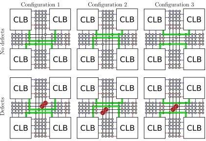
Figure 1.1: The rich pool of interchangeable resources in an FPGA provides many functionally equivalent configurations. For nominal, defect-free FPGAs, arbitrary selection is adequate. When defects are present, CSM enables us to select a configu-ration that best matches each chip.
Design-specific performance tweaks such as clock skewing [76, 74] and slack steal-ing can also provide delay improvements for nominal or lightly varysteal-ing devices. How-ever, these techniques do not address the complete failure of some switches that occurs at more energy efficient voltages.
1.3.1 Component-specific Mapping (CSM)
the freedom to discard bad resources for usable spares. We can use this freedom to adapt the mapping of a user circuit to the unique capacities of each target FPGA, i.e., CSM.
This concept was demonstrated in practice by Hewlett Packard in the context of the TERAMAC project [14]. To make it work, all FPGAs are thoroughly tested to locate defects, and the resulting information stored for later use. When an appli-cation is mapped (much like a computer program is compiled) for TERAMAC, the tools use the stored knowledge to work around defects. Mehta [59] demonstrated the ability of this form of knowledge-based specialization to tighten variation-driven energy margins. His results set an energy efficiency target for the present work (see Chapter 7).
This approach pre-emptively performs full custom mapping for each part of a user design for each target FPGA, performing considerable work to specialize nets which may not require the extra attention. In contrast, Lakamraju and Tessier [46] propose an incremental approach: work with the nominal configuration and only reroute nets affected by defects or disturbed by the rerouting of other nets. For small numbers of defects, they show that this approach produces a repair solution in a fraction of the time required for routing from scratch. The speedup comes largely from leveraging common solutions (i.e., the original pre-repair route) which account for most of the configurations of most nets (when defects are few). Taking this concept a step further, individual repair solutions may satisfy the needs of multiple chips with differing defect patterns (see Figure 1.2). Thus, we can save work by reusing repair solutions in addition to portions of the pre-repair configurations. Moreover, these single-net repair solutions can be pre-computed, eliminating the troublesome requirement that the FPGA loader also be capable of performing full routing.
CLB
CLB
CLB
CLB
(a)
CLB
CLB
CLB
CLB
(b)
CLB
CLB
CLB
CLB
(c)
Figure 1.2: (a) shows a design mapped on a healthy FPGA. A single repair solution addresses the different defects in FPGAs (b) and (c).
(a) Conventional FPGA configuration with a single path for each of three shown two-point nets.
(b) Configuration with path multiplicity. Each of the three nets is shown with two different paths (a green original path, and an orange alternative path). When configuring an FPGA, one of the two paths is selected for each net.
(c) Path selection for the three nets, used to work around three different defects.
(single FPGA configurations) amongst the chips in a multi-FPGA system (5 chips in an experimental BEE2) to find a functional overall configuration. Xilinx uses this idea for the EasyPath™program [42, 50, 86] to recover some value from chips that fail to meet normal production specs. Customer applications are matched to potentially defective FPGAs, using design-specific testing. Chips that pass are sold at a reduced rate to the respective customers with the guarantee of full performance and functionality of a standard FPGA, but only for the one specific application.
With CSM, a single design is compiled into different configurations with equivalent functionality to match the characteristics of specific FPGAs. We can also produce multiple equivalent mappings targeting coverage of avoidable defect patterns (again, consider the three example configurations in Figure 1.1) rather than the specific defect patterns of individual chips. The library of alternative configurations can be used much like the different system components of Hyder and the different applications in EasyPath™. However, in this case, the goal is to produce the same functionality in each chip.
Configuration multiplicity has been studied at a number of different scales [75], including the coarsest (full-chip bitstream multiplicity) [84, 56], coarse block multi-plicity [32] and shuffling (an intra-chip variant of Hyder’s approach), and multimulti-plicity at the level of paths or “two-point nets” (Trimberger [83], Campergher [9], Rubin [70]). Figure 1.3 shows a simplified example of path multiplicity.
Figure 1.4: CYA CAD flow vs. conventional flow
Chapter 7).
This dissertation describes Choose-Your-own-Adventure (CYA), my novel ap-proach to CSM, details the implementation I used to test it, and demonstrates its advantages.
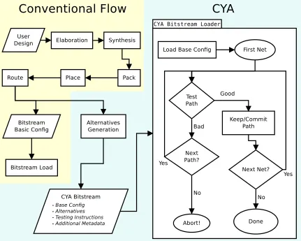
1.4 CYA: Path-Multiplicity Based CSM
The CYA process (Figure 1.4) matches conventional FPGA CAD flow until after the routing stage, at which point the conventional flow has a complete and fixed configuration. The next CYA stage is alternatives generation. One two-point net at a time, the alternatives generator searches the FPGA resource graph for other legal paths to connect that source/sink pair. This procedure processes each two-point net until the requested number of alternative paths are discovered, or until reasonable effort fails to reveal additional distinct paths. In general, one would request at least one alternative for each two-point net. In this work, most studies use a target of 64 alternatives.
The core of the alternatives generator was inspired by the popular routing al-gorithm Pathfinder [58]. It is built around shortest-path searches (Dijkstra [19] or
A∗ [31]), where costs that shift from one search to the next drive solutions towards
specific goals. For alternatives generation, the goals are first to do no harm, and second to produce a diverse set of paths to maximize the probability that at least one will work well for each chip.
To achieve the first goal, I constrain alternate paths to resources that are unused in the base route or only used by the originating net. It should be noted that these nets start with logic blocks (logic elements (LEs) or look-up tables (LUTs)). Therefore, these alternatives provide repair/swapping for both interconnect and logic.
The second goal, alternative diversity, is achieved by penalizing expansions that follow previously recorded alternatives.
Costi = (Costi−1+N odeCosts)
·(1 +P revAltCount·RepetitionP enaltyF actor)
(1.1a)
This common-prefix path penalty adds exponential pressure on the search to break away from the previous paths. An additional per-node usage penalty provides linear pressure to avoid previously used nodes, whether or not the paths to those nodes are part of previously recorded prefixes. These searches are repeated until the re-quested number of alternatives are generated or no new paths are discovered after several attempts, where the penalty factor is increased with each failed attempt. The alternative generation procedures are covered in depth in Section 4.2.3.
Once generated, alternatives are added to the bitstream (the “machine code” streamed into an FPGA to configure it), along with the conventional “base” route. The CYA bitstream may also include supplemental instructions for testing procedures or other information to assist the mapping process.
The CYA bitstream loader builds on the conventional loader, adding the support needed to select alternatives and to act on those decisions. The first step is to map the base configuration, much like a conventional loader. Next, the mapped FPGA is tested to verify proper functionality. Then, broken two-point nets are unmapped and each is repaired individually by mapping and testing its alternatives one after the other until one works. If any net runs out of alternatives, the loader reports failure and aborts.
The pre-computed alternatives focus on routed nets, that is, nets that send signals outside the originating cluster. Local nets, those that terminate entirely within the originating cluster, are simpler to remap on the fly. In the process of evaluating alter-natives for a routed net, the loader may remap local nets to any currently available LEs within the cluster.
provides a simple but complete testing regime.
Extending the loader to support testing of the circuit functionality at any specified fixed speed requires only a few minor changes. First, the modeled delays from the original routing are annotated into the bitstream. The annotated delay budgets are then adjusted to allow some nets to operate more slowly than modeled when this will not slow down the entire design (elaborated in Section 5.2.1). Finally, functionality testing is performed at a frequency related to the slack budget for each two point net. Delay optimization is achieved by performing complete, fixed-speed load/repair at various target delays, following a chosen search pattern (e.g., a binary search for the fastest workable speed). To provide delay budgets for each two point net at different clock frequencies, I simply scale the original budgets by the ratio of the current target delay to the modeled target delay recorded in the bitstream.
To optimize energy, delay optimizing load/repair is performed at various voltages, to select the most energy-efficient voltage at which the design functions properly. Further research may provide models to estimate the most efficient voltage; however, for my results (see Section 6.2), I assume power metering to directly identify the most efficient voltage rather than relying on approximations from other parameters.
1.5 Results
updated architecture that was used from that point forward.
The CAD stages in these experiments are based on an analogue of traditional CAD flow — synthesis, packing, placement, and routing (the yellow-shaded portions of Figure 1.4) — followed by simulated loading and analysis to measure area, delay, and energy. Additional stages provide data for full-knowledge routing and CYA (the blue-shaded portions of Figure 1.4). This CAD flow is feed-forward and intermediate results are preserved to be used for different experiments at later stages. For exam-ple, I only resynthesize a netlist when changing LUT size, but I use fixed synthesis, packing, and placements if I want to examine the impact of changing channel width.
Changes inVddor defect/variation patterns (i.e., comparing different chips) only affect
the final stage of the flow (loading for most experiments, routing for full-knowledge). Sections 4.5 to 5.1 explore the ability of CYA to address post-fabrication defects.
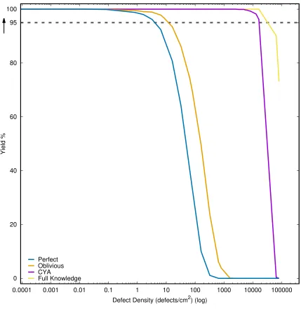
Figure 1.5 illustrates the resulting substantial yield improvements for des — CYA
maintains full yield at defect densities several orders of magnitude beyond both the point at which observable numbers of imperfect chips begin to appear, and the point at which oblivious mapping (use of a single static map) on those imperfect chips begins to experience failures. Across the full Toronto 20 benchmark suite, I saw no failed
loads at defect densities as high as 81 defects/cm2 (Table 4.10). Moreover, it is likely
that the rare failures at this defect density, as well as many of the failures at higher defect densities, may be addressed (as future work) with minor improvements to CYA, with complementary solutions (e.g., [46]), or by establishing testing methodologies to catch obviously irreparable combinations of defects. Consequently, it is significant
that, in my experiments, CYA maintains 95% yield up to 2400 defects/cm2 for all
Toronto 20 designs.
or broken, I ask whether that path functions fast enough to satisfy a prescribed delay budget and use this test to determine which paths are usable or need to be replaced with an alternative. The logic of the CYA repair process otherwise remains unchanged. The results of these experiments are reported in Sections 5.2 and 6.1. At the standard operating voltage for the 22nm technology used in these experiments
(Vdd = 0.8V), CYA provides only a small speed-up. However, at lower voltages, CYA
begins to substantially improve both total and parametric yield (yield of chips that
operate at a given speed). Figures 5.5 to 5.7 show examples of this behavior fordes.
These low-voltage parametric yield enhancements enable the most exciting capa-bility of variation tolerance: energy savings achieved through voltage reduction (Sec-tion 6.2). Lowering the voltage reduces dynamic energy consump(Sec-tion, but this comes at the cost of increasing variation-related faults and slowdowns. Conventionally-loaded chips are forced to run slower (at increasing cost in static energy), or fail to run at all. CYA repair substantially mitigates these effects, allowing both yield and energy recovery. Table 6.6 shows the energy reduction of CYA relative to conven-tional loading for all Toronto 20 designs (an average of 61%), while Table 6.7 shows the recovery of the energy lost to variations (an average of 70%).
Moreover, given that full-knowledge routing requires 7 orders of magnitude more load time to mitigate only 15% more of the energy cost of variations than CYA does (85%, compared to CYA’s 70%), it seems clear that CYA represents a cost/benefit sweet spot in the CSM energy savings landscape.
1.6 Pertinent Publications
The following publications of mine cover work discussed in or closely related to this dissertation:
1. Choose-Your-Own-Adventure Routing: Lightweight Load-Time Defect Avoid-ance [69, 70]
2. Component-Specific Mapping for Low-Power Operation in the Presence of Vari-ation and Aging [27]
3. Timing-Driven Pathfinder Pathology and Remediation: Quantifying and Re-ducing Delay Noise in VPR-Pathfinder [71, 72]
4. Limit Study of Energy & Delay Benefits of Component-Specific Routing [61]
5. Pitfalls and Tradeoffs in Simultaneous, On-Chip FPGA Delay Measurement [51]
6. Continuous Online Self-Monitoring Introspection Circuitry for Timing Repair by Incremental Partial-reconfiguration (COSMIC TRIP) [22, 23]
7. Quality-Time Tradeoffs in Component-Specific Mapping: How to Train Your Dynamically Reconfigurable Array of Gates with Outrageous Network-delays (DRAGON) [24]
95
0 20 40 60 80 100
0.0001 0.001 0.01 0.1 1 10 100 1000 10000 100000
Yield %
Defect Density (defects/cm2) (log) Full Knowledge
CYA Oblivious Perfect
Figure 1.5: Yield comparison of the following routing methodologies: requiring perfect chips (“perfect”), using static mapping on all chips (“oblivious”), using CYA mapping on all chips (“CYA”), and using full-knowledge routing on all chips (“full-knowledge”).
Yield figures are for des mapped to 1000 chips, using 22nm technology and a die
area of 9 million λ2 (4400µm2). All chips had 20% extra base tracks, 16 reserved
tracks, and single-driver interconnect, and the CYA mapping used 64 alternatives. Simulations were performed in VPR 5 [53].
1.7 Who Did What
The full-knowledge CSM work was a group project. Benjamin Gojman specialized in the implications for nanowire-based technologies. Nikil Mehta specialized in con-ventional and near-future technologies. Mehta’s work provided many of the detailed area, delay, and energy models used to produce the data presented throughout my dissertation.
My own modifications to VPR to support defects, variations, and knowledge-based routing provided a foundation for the full-knowledge research as well as the CYA project. Relevant code files are included with the electronic deposit of this dis-sertation. Hans Geisen and I jointly modified channel construction in VPR to enable reservation for repair solutions in directional interconnect [24, 23] (see Section 4.6.3). Hans Geisen also extended CYA into incremental [24] and online [22] variants.
1.8 Key Contributions
• CYA, a novel, lightweight, scalable methodology to achieve defect and variation mitigation
• Implementation of CYA, including preparatory components (generation of di-verse alternative paths) and FPGA load-time components
• Detailed performance characterization of CYA
– Comparison to conventional loading and DFVS
– Limit studies to characterize the quality of the CYA implementation and
Chapter 2
Setting
2.1 International Technology Roadmap for
Semi-conductors
The International Technology Roadmap for Semiconductors (ITRS), as the name implies, is a roadmap for the semiconductor industry. It is produced through the cooperation of companies that manufacture computer chips, companies that supply and produce materials and equipment for the manufacturers, and researchers (public, private, and academic). Its purpose is to set short-term and long-term goals for the industry and to identify the challenges that must be addressed to meet those goals. In short, the roadmap is the predominant authority on the research needs of the semiconductor industry.
Figure 2.1: Cartoon representation of a resistor. Free charges carry current from one end to the other.
2.2 Transistor Fundamentals
A brief review of the basic concepts of transistor technology will help illustrate the changing nature of the problems which arise with transistors at the 22 nm technology node and beyond.
Current computer chips consist mostly of field-effect transistors (FETs) and wiring to connect those transistors. A FET is an analog device, essentially just a variable resistor. In a normal resistor (Figure 2.1), relatively mobile “charge carriers”
(specif-ically, electrons) carry charges from one terminal to another. The resistance R of a
resistor is a function (Equation (2.1)) of its length L, its cross-sectional area W H
(width times height), the density of charge carriers, and how easy it is to move the charge carriers (mobility). The density and mobility of the charge carriers are jointly
represented in the single resistivity parameter ρ, a property of the material of which
the resistor is composed.
R=ρ L
W H (2.1)
Inserting this equation into Ohm’s law (V =IR), we get Equation (2.2), which relates
the current I through the resistor to the voltage V applied across its terminals.
I = W HV
ρL (2.2)
con-Tox
Tg
L
Gate
Source Drain
Oxide
Body
(a) Cross-section
L Gate
Source W Drain
(b) Top-down
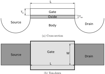
Figure 2.2: The basic structure of a metal-oxide semiconductor field-effect transistor (MOSFET).
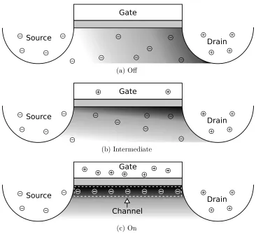
Gate
Source +Drain +
+ +
(a) Off
Gate
Source ++Drain +
+ + +
+ +
+
(b) Intermediate
Gate
Source Drain
Channel
+
+ +
+ + +
+ +
+ + +
+
+ ++ ++ ++
(c) On
Transistor current and delay can be approximated using Equations (2.3) [59]:
Isat =W vsatCox
Vgs−Vth−
Vd,sat
2
γ
(2.3a)
Isub=
W
LµCox(n−1) (VT)
2
e
Vgs−Vth nVT
1−e−VdsVT
(2.3b)
Ion=
Isat f or Vds =Vdd ≥Vth
Isub f or Vds =Vdd < Vth
(2.3c)
Iof f =Isub(Vgs = 0) =
W
L µCox(n−1) (VT)
2
e−nVTVth
1−e−VdsVT
(2.3d)
τp =
CVdd
Ion (2.3e)
These equations describe the current Ion that can flow between the source and
drain when the voltage Vds between these points (equal to the supply voltageVdd) is
above (Isat) or below (Isub) the threshold voltageVthfor the transistor. This threshold
voltage is defined as the minimum voltage that establishes a conductive channel that spans the full length of the transistor (connecting the source and drain terminals).
The delayτpis determined by the switched capacitanceC, the supply voltageVdd, and
the currentIon. In these equations,Vgs is the gate-source voltage difference and Vd,sat
is the drain saturation voltage, above which increases in the drain-source voltage no longer affect the current flow.
From this model we can begin to see how variations arise. Topological deviations,
such as errors in channel widthW or lengthL, alter resistance. Variation in thickness
of the oxide layer (the dielectric between the gate and the body forming a structure
with capacitance Cox) alter the strength of the field from the gate in the body, which
can also alter Vth and the slope factorn. Likewise, a change in the number of charge
carriers resulting from effects such as random dopant fluctuation (RDF) will make
the charge carrier mobility µ. Crystal defects, impurities, and local temperature variations can also affect these parameters, as well as changing the charge carrier
saturation velocityvsat, its associated constantγ, and the thermal voltageVT. Finally,
Vth can also be changed by the induction of a field in the body (typically from below)
which counters or assists the field from the gate. When done deliberately, this last effect is called “body biasing” (as discussed in Section 3.2.2).
Fabrication variations can result not only in parametric deviations, but also in hard defects. For example, if the gate material extends past the oxide, it may short with one of the terminals. A loose particle might block dopant injection and then wash away before the next fabrication step. Errors in the substrate can alter the electrical properties in the body or induce gross geometric errors. In short, transistors require very fine control of the production environment and processes to achieve reliable outcomes.
2.3 What Has Changed?
Year 2005 2006 2007 2008 2009 2010 2011 2012
DRAM 1
2 Pitch (nm) 80 70 65 57 52 45 40 36
3σVdd 10 10 10 10 10 10 10 10
3σVth RDF (min size) 24 29 31 35 40 40 40 58
3σVth total (min size) 26 29 33 37 42 42 42 58
3σVth total (typical logic) 16 18 20 20 20 26
3σ critical dimensions 10 10 12 12 12 12 12 12
3σ circuit performance 41 42 46 48 49 51 60 63
Year 2013 2014 2015 2016 2017 2018 2019 2020
DRAM 1
2 Pitch (nm) 32 28 25 22.5 20 17.9 15.9 14.2
3σVdd 10 10 10 10 10 10 10 10
3σVth RDF (min size) 58 81 81 81 81 112 112 112
3σVth total (min size) 58 81 81 81 81 112 112 112
3σVth total (typical logic) 26 36 36 36 50 50 50 50
3σ critical dimensions 12 12 12 12 12 12 12 12
3σ circuit performance 63 63 63 63 65 66 69 69
Table 2.1: As scaling continues, cost-effective management of process variation is expected to become increasingly difficult. Consequently, if Moore’s Law is to continue, an increasing burden of variation tolerance is projected to be left to post-fabrication solutions.
Except for critical dimensions, all variability (σ) values are given as a percentage
(%) of nominal. Topological variability is given as a percentage of the dimensions of a minimum-sized transistor as opposed to the design-nominal dimensions for each transistor. This data is compiled from the 2005, 2007, and 2009 ITRS reports.[37, 38, 39]
Dopant implantation is a Poisson process [78]. For large transistors with many dopants, the size of any variations will be negligible relative to the total dopant population. Thus, for older technologies the total number of dopants and their dis-tribution in the body of a transistor are consistent enough that variation is not a concern. Newer technologies are a different story.
RDF is a hard problem to solve and the resulting variation persists through fab-rication. Table 2.1 shows this trend in action. At 80 nm (where the ITRS began
(system supply voltage)1 and topological variations. However, process improvements
hold Vdd and topological variations steady while the impact of RDF grows. In the
ITRS projections for 2011, dopant fluctuations are expected to account for half of performance variations [40].
RDF cannot be detected visually, thus visual inspection is insufficient to identify slow circuits. A slow circuit may not fail a slow signal propagation test, as the bits do get through eventually. It also will not trigger a quiescent current test and may even have favorable power characteristics. To catch an RDF-related parametric defect may require testing a circuit in operation at full speed. That means we may lose the cost savings of early detection of bad dies, assuming we can catch such defects at all.
These issues are not a surprise, as the emergence of RDF as a significant limiter was predicted almost half a century ago by Hoeneisen and Mead [33]. If anything, the surprise (at least from a 1971 perspective) is that reliable 14nm circuits (e.g., Intel’s Broadwell processors) can be built at all.
2.4 Summary
Killer defects are getting smaller and harder to identify visually. We also must worry about invisible parametric defects that are even harder to identify. In short, “fabrica-tion of chips with 100% working transistors and interconnects becomes prohibitively expensive” [39, Design]. While it is important to continue improving manufacturing, post-fabrication defect tolerance can reduce the burden of perfection, thereby reduc-ing the cost of developreduc-ing future technologies. Lookreduc-ing forward, these strategies may be key enablers for otherwise impractical or even impossible technologies.
1 V
dd must be raised to compensate forVthvariation, thereby increasing the power consumption
Chapter 3
Current Solutions
Defect tolerance and variation tolerance in field-programmable gate arrays (FPGAs) (and logic in general) have been studied for over a decade (several decades for gen-eral logic). Many solutions have been published to address various aspects of these problems.
There are several categories of variations, which are typically addressed with dif-ferent solutions:
• Die-to-die variations and larger scale (e.g., wafer-to-wafer) variations have a uniform impact on a die. Techniques (including my own) that address within-die variations have little or no impact on these large scale variations.
• Spatially-correlated variations are non-systematic variations that result from sources that affect areas larger than individual transistors and wires. For cor-related variations, solutions may leverage statistical knowledge about the vari-ation distribution to avoid multiple likely bad devices at once. For example, if one look-up table (LUT) is identified as particularly slow, a placer might avoid adjacent LUTs, expecting them to be slow as well. Random dopant fluctuation (RDF) is not thought to result in spatially-correlated variations.
• Random variations are the variations that are not systematic and are indepen-dent of the variations in nearby devices. Some of the most significant sources of random variation in current and projected future fabrication (such as RDF) op-erate independently on individual transistors. For FPGAs, random variations and, likewise, random defects, are an important motivation for component-spe-cific mapping (CSM).
In addition to variations (which result in slow components, here referred to as “parametric defects”), my work, along with many of the techniques listed in this chapter, addresses the presence of completely non-functional components (“faults”) that result from physical defects. “Fault tolerance” is often used to describe both faults resulting from persistent physical defects and transient faults.
Techniques that target persistent faults focus on finding and eliminating defects. TMR can also be used to address persistent faults. My research addresses persistent faults from physical defects and parametric defects (i.e., variations), but not transient faults.
3.1 Chapter Organization
The existing solutions discussed in this chapter are organized into three categories:
1. Solutions that address low-amplitude variations only (Section 3.2).
2. Solutions that will not effectively solve large numbers of defects (Section 3.3).
3. Solutions that are effective for both variations and defects and are therefore more comparable to my work (Section 3.4).
3.2 Techniques That Address Variations Only
Much recent variation tolerance research focuses on techniques that do not migrate logic and routing from bad resources to better resources. These techniques are gen-erally limited to reducing specific small margins, and do not address hard defects. Therefore, these techniques are not fully comparable to my work; however, each is described briefly below.
3.2.1 Statistical Static Timing Analysis (SSTA)
For FPGAs, a number of publications examine the value of adding SSTA to the clus-tering, placement, and routing stages of conventional FPGA CAD [49, 77, 52, 44]. According to Mehta [60], the most optimistic results so far predict a 12.6% improve-ment in timing yield (the fraction of chips that run correctly at a given frequency)
for 3σVth/µVth = 10%.
3.2.2 Body Biasing
Nabaa et al. [63] explored regional biasing in FPGAs that is similar to the approach proposed for processors in [80]. (Resource overhead makes body biasing too costly to apply to individual transistors.) Nabaa’s approach characterizes each physical FPGA tile (a logic block and nearby routing resources) to calibrate for process variation. That calibration is combined with the slack of the logical circuit (the user design loaded onto the FPGA). Body biasing is applied to each tile to improve performance where necessary and to reduce power consumption in regions with extra slack. Be-cause biasing is applied regionally, it is most effective for variations which benefit from uniform tuning (e.g., spatially-correlated variations). With an estimated 1.6% area
overhead, Nabaa’s simulations achieve a 30% reduction in σVth and a 78% reduction
in σpower for the modeled 130nm technology. However, with high degrees of random
variation (e.g., RDF), as are seen in smaller-pitch technologies, the advantages of biasing are limited by the most extreme transistors — tuning for one transistor may cause another in the region to fail.
3.2.3 Clock Phase Skewing and Slack Stealing
for signal propagation changes. For example, if a sink latch is slightly early, the signal must propagate from the source to that sink in less than a full clock cycle. In certain circumstances such skews may be used to effectively increase the clock period for a particularly slow chain of logic without slowing down the rest of the chip [76]. Multiple clocks and local phase shifting can be used compensate for variations in logic and the clock distribution network [74]. However, this technique is limited not only to adjustments on the order of the clock period, but also to the available delay that can be shifted from one circuit to another. It cannot compensate for switches that are broken or that slow down the circuit beyond these limits. To address these more extreme cases, it is preferable to be able to avoid the bad switch entirely.
3.3 Techniques That Address Low Defect Rates
3.3.1 Multiple Bitstreams
3.3.2 EasyPath™
The Xilinx EasyPath™ [86, 42] program is similar to the multiple-bitstream approach. Multiple bitstreams are tested on each FPGA to find one that works. However, for EasyPath™, multiple FPGAs are also tested for each bitstream to find FPGAs that match the needs of the customer. The purpose of this program is to reduce waste by finding applications for chips that fail quality testing and cannot be sold as fully functioning FPGAs. While EasyPath™ is successful at achieving this goal, it does not offer a general solution to the problem of mapping an arbitrary application to an arbitrary imperfect chip.
3.4 Techniques That Address High Defect Rates
The techniques discussed in this section attack similar aspects of the defect/variation problem to those addressed by my own work. Many are already used in common practice and show significant benefits; however, Choose-Your-own-Adventure (CYA) has certain distinct advantages relative to each.
3.4.1 Modular Redundancy
A seminal work on defect tolerance is John Von Neumann’s “Probabilistic Logics and the Synthesis of Reliable Organisms from Unreliable Components” [65], in which he introduced and analyzed the use of redundancy, particularly triple modular redun-dancy (TMR). TMR continues to be a standard defect tolerance solution, particularly in critical systems and in devices operating in harsh environments where single-event upsets (SEUs) are common.
applica-tions. Documents from Xilinx [10] and Actel [2] highlight architectural features that aid in the integration of TMR into logical circuits. Pratt et al. [67] developed a tool to automatically add TMR selectively to those portions of a design that will most benefit from redundancy. At the physical circuit level, Actel produced radiation-hardened parts [18] that use TMR to protect particularly sensitive structures. At Xilinx, Trimberger [82] patented specific structures that may be used for TMR or to enhance functionality when redundancy is not needed.
TMR comes with high costs: a minimum of 200% area and power overhead are needed for almost all applications, and the inline voting process also adds delay. TMR also does not scale well with increasing defect rates — Von Neumann’s analysis shows that overhead grows exponentially with the number of simultaneous failures the system is designed to tolerate. Consequently, more modern techniques generally prefer solutions with lower overhead and focus on addressing specific failure modalities rather than generic faults.
3.4.2 Hardware-Sparing In-Factory Repair
Another approach to defect tolerance is to perform the defect tolerance behind the scenes, always presenting the end system with the appearance of a perfect component. Column sparing has long been used to improve yield for memories [21]. Post-fabrication testing identifies columns and rows that contain defects. A permanent alteration (e.g., blowing out a fuse) disables the offending region and remaps the array to fill the gap. The shipped memories appear defect-free to the consumer.
These implementations of sparing result in additional area and delay overhead.
For an 80% yield target and an interconnect defect rate of around 2·10−4 defects
per wire segment, Yu and Lemieux estimate their design requires 50% area overhead, while the coarse-grained row sparing technique requires over 100% area overhead. By comparison, Figure 4.7 shows that a CYA solution attains the same yield at defect
rates an order of magnitude higher, with only∼20% area overhead. The interconnect
defect density in Yu and Lemieux’s work is approximately 100 defects/cm2 in the
45nm technology they used, corresponding to∼400 defects/cm2 in my 22nm studies.
Table 4.10 shows CYA producing 95% yields at defect densities an order of magnitude higher or more, in simulated chips which contain not only interconnect defects, but also logic defects.
The delay effects of CYA and sparing methods also differ. In both methods, the area overhead imposes an inherent delay burden, so CYA’s reduced area offers a relative advantage here. Moreover, unlike sparing methods, CYA does not need to pay the delay costs associated with adding in-path bypass circuitry.
3.4.3 Avoiding Faults
The multiple-bitstreams solution (Section 3.3.1) does not repair defects, nor does it hide them. It prevents faults by using non-defective devices and avoiding defective devices.
the long runtime for conventional FPGA mapping tools. To accelerate the mapping process, TERAMAC employed a richer and more regular interconnect architecture than conventional FPGAs [3], trading density for mapping speed.
Local substitution of resources can potentially reduce or avoid the high cost of complete FPGA remapping at the expense of accepting less-optimal mappings. Lach introduced a design style for FPGAs that reserved one or more logic blocks in an
N × N tile so that defects could be repaired with local sparing [45]. Lakamraju
and Tessier note that reserving spare LUTs in an island-style cluster also allows local repair of logic [46].
Given the domain [89, 81] style of most FPGAs, one simple way to generate alternatives is to reassign entire domains (e.g., [97]). With a small number of defects, a comparable number of spare domains could be used to replace domains that contain defects with defect-free domains. Domain swapping is very coarse-grained and, similar to the multiple full-bitstreams solution, this large repair granularity does not take full advantage of inherent FPGA configurability.
Chapter 4
CYA
{
{
{
Reserved TrackBase Tracks ChannelFigure 4.1: Channel with four tracks, one of which is reserved. Three nets saturate the three base tracks.
4.1 Inspiration
The name Choose-Your-own-Adventure is an homage to the eponymous Choose Your Own Adventure novels [66]. Those books are structured around user decisions. This device enables a single immutable hardcopy book to provide many variants of a story, tailoring the plot, on each read-through, to the whims of the reader. Likewise, in Choose-Your-own-Adventure bootstrapping, a single immutable field-programmable gate array (FPGA) bitstream provides choices which result in loaded configurations tailored to the peculiarities of each individual consumer FPGA.
4.1.1 Illustrative Example
most one track), the defect(s) will either be in the fourth track and will not disturb the default routes, or it/they will upset a single route, forcing that route to use the alternate path on the fourth track.
We can expand the notion of tracks to domains. By domains, I refer to architec-tures where the interconnect network is partitioned into independent sets of routing resources (e.g., [89]). With domains, the initial track choice leaving a source block determines the track that will be used when entering the destination block. The in-dependence property of domains means that when we reserve a domain, we do not affect the rest of the network. Resources that are part of the reserved domain are
not available to the base domains and vice versa. Now we can look at a whole chip
and say that default paths are routed in the base domains and alternatives are routed on the reserved domain and unused portions of the base domains. This allows us to guarantee that an FPGA with a single defect anywhere in the interconnect has an unused alternate route that will avoid the defect.
4.2 CYA Components
I now describe CYA bitstream composition, generation, and loading. Figure 4.2 (repeating Figure 1.4) provides a roadmap for this discussion.
4.2.1 CYA Bitstream
Elaboration Synthesis
Pack Place Route
Alternatives Generation
Bitstream Load
CYA Bitstream Loader
Load Base Config First Net
Test Path
Keep/Commit Path Good
Next Net? Yes
Done No Next Path?
Abort! Yes
No Bitstream
Basic Config
- Base Config - Alternatives - Testing Instructions - Additional Metadata
Bad User
Design
Conventional Flow CYA
CYA Bitstream
The CYA bitstream is a list of two-point nets each with:
• a base path configuration
• a list of alternatives
• a set of testing instructions
• optional metadata such as the delay budget (used in Chapters 5 and 6)
This means that bitstream programming is ordered by logical functions rather than by physical location on the FPGA. For fabrics where the configuration bits are not randomly addressable, such as Virtex frames [91, 93], I assume the presence of a translator (see Section 4.2.4) that can add or remove the portion of the input path that applies to the configured frame.
The base route is a normal FPGA route prepared using only base tracks.
An alternative is a different path from the base route that can be used for defect
avoidance. It consists of a set of resources that connects a single source to a single sink (i.e., a two-point net) that differs by at least one resource from the corresponding path found in the base route. Alternative paths may use both the reserved spare resources and any non-reserved resources that were left unused by the base route, and are forbidden from using any resources which are part of the base paths of other nets. This guarantees that we are free to switch from a base path to any of its alternative paths without interfering with any of the base routes.
testing for more complex cases (e.g., look-up table (LUT) and Flip-Flop testing, or
testing for bridging) and to simplify the design of the loader, I embedtest instructions
in the bitstream. In the simplest scheme described here, multi-point nets are handled by checking each two-point net independently.
4.2.2 Routing
Elaboration Synthesis
Pack Place Route
Alternatives Generation
Bitstream Load
CYA Bitstream Loader
Load Base Config First Net
Test Path
Keep/Commit Path Good
Next Net? Yes
Done No Next Path?
Abort! Yes
No Bitstream
Basic Config
- Base Config - Alternatives - Testing Instructions - Additional Metadata
Bad User
Design
Conventional Flow CYA
CYA Bitstream
The base route can be generated with a standard FPGA router such as Pathfinder [58]. The only differ-ence is that we may choose to reserve some resources solely for use in the preparation of alternate paths. The router must therefore be capable of acknowledg-ing these resources as beacknowledg-ing “off limits” to the base route.
4.2.3 Alternatives Generation
Elaboration Synthesis
Pack Place Route
Alternatives Generation
Bitstream Load
CYA Bitstream Loader
Load Base Config First Net
Test Path
Keep/Commit Path Good
Next Net? Yes
Done No Next Path?
Abort! Yes
No Bitstream
Basic Config
- Base Config - Alternatives - Testing Instructions - Additional Metadata
Bad User
Design
Conventional Flow CYA
CYA Bitstream
Alternatives are paths that must not conflict with the base route. We want a diverse (see Section 4.3) set of alternatives for each base path, to maximize the op-portunity for defect avoidance. To encourage this di-versity, I associate a cost with resource usage similar to Pathfinder resource costs. This allows me to use
repeated calls to a shortest path search to find different routes as long as I
up-date the cost of each resource in the graph as it is used. This Resource-Cost
Algo-rithm is shown in Algorithm 4.1. Pathfinder-based routers can easily be modified
is: cost = alternatives using + 1. In Section 4.3 I note the shortcomings of the
Resource-Cost Algorithm and introduce a more sophisticated Path-Cost Algorithm.
Algorithm 4.1: Resource-Cost Algorithm for alternatives generation
input :Route base route
output:Bitsteam C
foreach Resource R∈ {base route}do Disable R ;
foreach N et N ∈ {base route.nets} do
foreach GraphN ode sink ∈N.sinksdo
C.addP ath(N, N.base path(sink));
foreach Resource R∈ {all Resources} do
R.alternatives using = 0;
foreach Resource R∈ {N.base path(sink)}do
Enable R;
for i=1 to number of alternatives do
P ath P ←FindShortest(N.source,sink);
C.addAlternative(P);
foreach Resource R ∈P do
R.alternatives using+ +;
foreach Resource R∈ {N.base path} do
Disable R;
![Fig ur e4 .8 : Yie ld v s . de f e c tC o s t Alg o r it hm (po pula t e d C - B o x e s , VP Rr a t ef o rt heR e s o ur c e - C o s tAlg o r it hm a nd t heP a t h- d e s , noe x t r aba s e t r a c k s , 2 0 % r e s e r v e d t r a c k s , 5a lt e r na t iv e s , f ully4 .3[5 ], mult i- dr iv e r int e r c o nne c t , 1 0 0c hips ) .](https://thumb-us.123doks.com/thumbv2/123dok_us/9239061.1459536/83.612.111.539.137.566/fig-yie-alg-pula-talg-ully-mult-hips.webp)
![Fig ur e4 .1 6 : An e x a mples ho w n he r eT he S- B o xmo de le d in VP RFP G A t ile( aC L Ba nd t hes ur r o undingint e r c o nne c t ) a s5[5 3 ]](https://thumb-us.123doks.com/thumbv2/123dok_us/9239061.1459536/107.612.113.537.111.550/fig-mples-vp-rfp-ile-ba-hes-undingint.webp)
![Fig ur e4 .2 0 : Yie ld v s . de f e c t r a t ea lt e r na t iv e s , VP Rw it h noa nd br e a k sf o r no mina l ( pe r f e c t c hips ) , o bliv io us ( ba s er o ut ea lt e r na t iv e s ) , a nd C YA r o ut ing , c o mpa r ingt heimpa c t s o f br idg e s ( s ho r t s )( d e s , 2 2 nm t e c hno lo g y , 2 0 % e x t r aba s et r a c k s , 1 6r e s e r v e d t r a c k s , 6 45[5 3 ], s ing le - dr iv e r int e r c o nne c t , 1 0 0 0c hips ) .](https://thumb-us.123doks.com/thumbv2/123dok_us/9239061.1459536/113.612.115.537.129.560/fig-yie-mina-hips-bliv-ingt-heimpa-hips.webp)
![Fig ur e 4 .2 1 : Yie ld v s . de f e c t r a t e f o r de f e c t s in C L Binput buff e r s (no lo g y , 2 0 % e x t r a ba s e t r a c k s , 1 6 r e s e r v e d t r a c k s , 6 4 a lt e r na t iv e s , VP Rdr iv e r int e r c o nne c t , 1 0 0 0 d e s , 2 2 nm t e c h-5 [5 3 ], s ing le -c hips ) .](https://thumb-us.123doks.com/thumbv2/123dok_us/9239061.1459536/114.612.114.539.134.568/fig-yie-binput-bu-rdr-int-ing-hips.webp)
