IJEDR1702243 International Journal of Engineering Development and Research (www.ijedr.org) 1547
RLC Parameter Extraction and Step Input
Response Analysis of Coupled High Speed
Distributed VLSI Interconnects
1
Hitlendra Pratap Singh,
2Dr. G.S. Virdi
1
Assistant Professor,
2Director Formerly Ex. Scientist-G Microelectronics CEERI, Pilani
Meerut Institute of Engineering & Technology, Meerut, India
Abstract-
In this paper,mathematicalformula are suggested to determine inductance and capacitance values and analysis of step input response of RLC coupled high speed distributed interconnects assuming the length of the line as finite and semi finite lines as well. The values of distributed resistance, capacitance, and inductance are calculated at different technology node 32nm, 45nm, 65nm, 90nm, 130nm, and 180nm. .In addition, the effect of technology and design parameters on the resistance, capacitance, and inductance of the distributed interconnects.Index Terms-Transmission line, Semi-infinite line, Finite line, Time domain analysis, Technology node
I. INTRODUCTION
Due to scaling down in process technologies into DSM crosstalk and its effects is a major issue in On-chip high speed VLSI interconnects, therefore, crosstalk and its effects are a serious issue in the system performance. Two crosstalk fault effects, mainly, glitch and crosstalk induced delay, The crosstalk-induced delay is found to be superposition of the induced glitch and the applied signal at the victim line, and this effect is more important in affecting the circuit performance. With the scaling of semiconductor, technologies delay time of high speed interconnects are becoming comparable with clock cycles. In other word, it is possible for the voltage through an interconnect caused by a near end transition, not to completely settle before the next transition begins. The remaining voltage through line considered as an initial condition in the computation of transient response caused by the next transition. With aggressive technology scaling, the local interconnect has become more resistive, and capacitive. The global interconnect has become more inductive. As per ITRS (2011) global wire delay increases and gate delay decreases with scaling [3].
According to the most widely used analytical delay model proposed by Sotiriadis et al. [2] and [3], the delay of the ith wire ( ∈ {1, 2, … … , 𝑛}) of an n-bit bus is given by:
𝑇𝑖= {
𝜏0[(1 + 𝜆)∇21 – 𝜆∇1∇2 ], 𝑖 = 1
𝜏0[(1 + 2𝜆)∇2𝑖– 𝜆∇𝑖(∇𝑖−1 + (∇𝑖+1 ]
𝜏0[(1 + 𝜆)∇2𝑛– 𝜆∇𝑛∇𝑛−1 ], 𝑖 = 𝑛
, 𝑖 ≠ 1, 𝑛
Where λ is the ratio of the coupling capacitance between adjacent wires and the ground capacitance of each wire, 𝜏0 is the intrinsic delay
of a transition on a single wire, and ∇𝑖 is 1 for 0→1 transition, -1 for 1→ 0 transition, or 0 for no transition on ith wire.
IJEDR1702243 International Journal of Engineering Development and Research (www.ijedr.org) 1548 Fig. 1 illustrates the schematic views of 5-wire Bus in which central wire act as victim line and in adjacent to line two lines are aggressor line above and below to this line respectively.
Fig. 1 Physical view of wiring of 5-bus network [1].
Three wire RLC modeled interconnect network with both coupling capacitance and mutual inductance shown below in Fig. 2
Fig. 2 3-Bus RLC Interconnect model with coupling capacitances and mutual inductances [1].
II. RLC PARAMETERS EXTRACTION
The circuit parameters are extracted using the IBM Electromagnetic Field Solver Suite Tools (EIP) [17] for the 32nm, 45nm, 65nm, 90nm, 130nm, and 180nm technology nodes [18-21] for the interconnect parameters tabulated in table 1. The operating frequency is 1 GHz with 100ps rise and fall transition times. The supply voltage is 1.8, 1.5, 1.2, 1, 0.95, and 0.9 V for the 180nm, 130nm, 90nm, 65nm,45nm, and 32nm technology nodes, respectively.
IJEDR1702243 International Journal of Engineering Development and Research (www.ijedr.org) 1549 The interconnect line resistance is
𝑅 =
𝜌𝐿𝑊𝑇 where ρ, L, W, and T are the resistivity, length, width, and thickness of the interconnect
respectively.
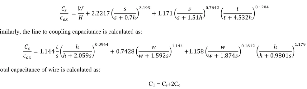
The line to substrate capacitance (area and fringe flux to the underlying plane) is calculated as:
𝐶𝑠
𝜖𝑜𝑥
=𝑊
𝐻 + 2.2217 (
𝑠 𝑠 + 0.7ℎ)
3.193
+ 1.171 ( 𝑠
𝑠 + 1.51ℎ)
0.7642
( 𝑡
𝑡 + 4.532ℎ)
0.1204
Similarly, the line to coupling capacitance is calculated as:
𝐶𝑐
𝜖𝑜𝑥
= 1.144𝑡 𝑠(
ℎ ℎ + 2.059𝑠)
0.0944
+ 0.7428 ( 𝑤
𝑤 + 1.592𝑠)
1.144
+1.158 ( 𝑤
𝑤 + 1.874𝑠)
0.1612
( ℎ
ℎ + 0.9801𝑠)
1.179
Total capacitance of wire is calculated as:
CT = Cs+2Cc
Where𝜀𝑜𝑥, h, and s are the oxide permittivity, distance, from interconnect to the substrate, and spacing between adjacent interconnects,
respectively.
Now, the closed form expressions for the self and mutual inductance of a line , respectively are;
𝐿𝑠=
𝜇𝑜
2𝜋𝐿 [𝑙𝑛 ( 2𝐿 𝑤 + 𝑡) +
1
2+
0.22(𝑤 + 𝑡)
𝐿 ]
and
𝐿𝑚=
𝜇𝑜
2𝜋𝐿 [𝑙𝑛 ( 2𝐿
𝑑)
−1
+𝑑
𝐿]
Where𝜇𝑜, d are magnetic permeability of free space and the center-to-center distance between two adjacent interconnects.
Table 1
Interconnect Parameters for 32nm, 45nm, 65nm, 90nm, 130nm, and 180nm technology nodes.
Interconnect Physical Parameters
Technology nodes
32nm 45nm 65nm 90nm 130nm 180nm
Width (µm) 0.3 0.40 0.45 0.5 0.6 0.8
Spacing (µm) 0.3 0.40 0.45 0.5 0.6 0.8
Thickness (µm) 0.504 0.72 1.2 1.2 1.20 1.25
Height (µm) 0.2 0.2 0.2 0.3 0.45 0.65
Ρ(10-8)Ωm 2.2 2.2 2.2 2.2 2.2 2.2
K 1.5 2 2.2 2.8 3.2 3.5
VDD 0.9 0.95 1 1.2 1.5 1.8
The operating frequency is 1GHz with 100ps rise and fall transition time.
III. TRANSIENT RESPONSE OF FINITE DISTRIBUTED
(1) STEP INPUT RESPOSNSE TO FINITE DISTRIBUTED RLC MODELED INTERCONNECT LINE [2].
IJEDR1702243 International Journal of Engineering Development and Research (www.ijedr.org) 1550 Fig. 4 Distributed RLC interconnect of length L driven by a step input [2].
The 1-D linear partial differential equation (PDE) for the next lossy transmission line. The distributed RLC model consists of a 1-D voltage equation:
𝜕2𝑉
𝜕𝑋2= 𝑟𝑐
𝜕𝑉 𝜕𝑡 + 𝑙𝑐
𝜕2𝑉
𝜕𝑡2
Where r, c, and, l are the resistance, capacitance, and inductance per unit length, respectively. The boundary conditions for the RLC modeled interconnects are as follows:
𝑉(𝑥, 0) = 𝐹(𝑥); 𝑉(0, 𝑡) = 𝑈0
𝑉𝑋(𝐿, 𝑡) = 0 ; 𝑉𝑡(𝑥, 0) =
1 √𝐿𝐶
Where F(x) is the initial voltage of the point x and U0 is the high-level amplitude of the step signal. In addition, U satisfies the equation:
𝜕2𝑈
𝜕𝑋2= 𝑟𝑐
𝜕𝑈 𝜕𝑡 + 𝑙𝑐
𝜕2𝑈
𝜕𝑡2
In addition, the conditions:
𝑢(0, 𝑡) = 0; 𝑢𝑥(𝐿, 𝑡) = 0
𝑢(𝑥, 0) = 𝑓(𝑥) − 𝑢0
𝑢𝑡(𝑥, 0) =
1 √𝐿𝐶
As the variable voltage, there is infinite no. of solutions for u satisfying the boundary conditions as
𝑢𝑛(𝑥, 𝑡) = 𝑠𝑖𝑛𝑝𝑛𝑥 (𝐴𝑛∗𝑒𝑚1𝑡+ 𝐵𝑛∗𝑒𝑚2𝑡),
Where𝑃𝑛= (2𝑛−1)𝜋
2𝐿 ; here m1 and m2 are determined by
𝑚1=
−𝑟𝑐 + √𝑟2𝑐2− 4𝑙𝑐𝑝 𝑛2
2𝑙𝑐
𝑚1=
−𝑟𝑐 − √𝑟2𝑐2− 4𝑙𝑐𝑝 𝑛2
2𝑙𝑐
Now, the solution of the RLC distributed line voltage equation is as:
𝑣𝑅𝐿𝐶(𝑥, 𝑡) = 𝑢0+ ∑
2 𝐿(𝑚2− 𝑚1)
∞
𝑛=1
𝑠𝑖𝑛𝑝𝑛𝑥 (∫ (𝑚2 𝐿
0
𝑓(𝑥) − 𝑚2𝑢0−
1
√𝐿𝐶) 𝑠𝑖𝑛𝑝𝑛𝑥𝑒
𝑚1𝑡
+ (∫ (𝑚1 𝐿
0
𝑓(𝑥) − 𝑚1𝑢0−
1
√𝐿𝐶) 𝑠𝑖𝑛𝑝𝑛𝑥𝑒
IJEDR1702243 International Journal of Engineering Development and Research (www.ijedr.org) 1551 (2) STEP INPUT RESPONSE TO DISTRIBUTED SEMI INFINITE RLC INTERCONNECT[2]:
The voltage signal through the semi-infinite interconnects satisfies the following expression:
𝜕2𝑣
𝜕𝑥2= 𝑟𝑐
𝜕𝑣 𝜕𝑡+ 𝑙𝑐
𝜕2𝑣
𝜕𝑡2
The initial conditions are:
𝑣(0, 𝑡) = 𝑈0 ; 𝑣(𝑥, 0) = 𝑓(𝑥); 𝑎𝑛𝑑𝑣𝑡(𝑥, 0) =
1 √𝑙𝑐
Using AMN simplification method, one find 𝑤 = 𝑈0 and
𝑈(𝑥, 𝑡) = ∫ 𝑠𝑖𝑛𝑝𝑥[𝐴(𝑝)𝑒𝑚1𝑡+ 𝐵(𝑝)𝑒𝑚2𝑡] ∞
0
𝑑𝑝
Where A(p) and B(p) are
𝐴(𝑝) = 2
𝜋(𝑚1− 𝑚2)
( 1
√𝑙𝑐𝑁(𝑝) − 𝑚2𝑀(𝑝))
𝐵(𝑝) = 2
𝜋(𝑚1− 𝑚2)
(𝑚1𝑀(𝑝) −
1
√𝑙𝑐𝑁(𝑝))
Where 𝑁(𝑝) = ∫ 𝑠𝑖𝑛𝑝𝑣𝑑𝑣0∞ 𝑎𝑛𝑑𝑀(𝑝) = ∫ [𝑓(𝑣) − 𝑈0]𝑠𝑖𝑛𝑝𝑣𝑑𝑣
∞
0
IV. CONCLUSION
The motive of this paper is to extract the values of resistance, capacitance, inductance, and mutual inductance at different technology nodes like 32nm, 45nm, 65nm, 90nm, 130nm, and 180nm given in table 2 corresponding to used specification given in table 1. The operating frequency is 1 GHz with 100 ps rise and fall transition times. The supply voltage is 0.9, 0.95, 1, 1.2, 1.5 and 1.8 respectively.
TABLE -2
Line parameters calculated at 32nm, 45nm, 65nm, 90nm, 130nm, and 180nm technology nodes Interconnect
Physical Parameter
Line Parameter R(Ω/m
m)
L(nH/ mm)
Cs(fF /mm)
Cc(fF/ mm)
CT(fF/ mm) 32nm 145.5 1.8 40.68 35.92 112.5 45nm 76.39 1.74 67.94 45.58 165.1 65nm 40.74 1.66 82.03 73.22 228.5 90nm 36.66 1.653 82.94 88.37 259.7 130nm 30.55 1.64 79.13 89.44 258.1 180nm 22 1.615 80.69 81.54 243.7
IJEDR1702243 International Journal of Engineering Development and Research (www.ijedr.org) 1552 TABLE-3
L W S T
R
Cs
Cc
Ls
Lm
V. ACKNOWLEDGEMENT
The author of existing research work is Ph.D scholar in I.K. Gujral P.T.U. Jalandhar and whole research work is concerned to Ph.D work.
REFERENCES
[1] A. Roy, J. Xu, andM. H. Chowdhury, “Analysis of the impacts of signal slew and skew on the behavior of coupled RLC interconnects for different switching patterns,” IEEE Trans. Very Large Scale Integr. (VLSI) Circuits, vol. 18, no. 2, pp. 338–342, Feb. 2010.
[2] Amir Reza BaghbanBehrouzian and Nasser Masoumi,“Analytical Solutions for Distributed Interconnect Models—Part I: Step Input Response of Finite and Semi-Infinite Lines”, IEEE Transactions on Very Large Scale Integration (VLSI) Systems, Sept. 2, 2013,
[3] InternationalTechnology Roadmap for Semiconductors. (2011)
[4] PP. 1-11.J. Zhang and E. G. Friedman, “Crosstalk modeling for coupled RLC interconnects with application to shield insertion,” IEEE Trans. Very Large Scale Integr. (VLSI) Circuits, vol. 14, no. 6, pp. 641–646, Jun. 2006.
[5] A. Vittal and M. Sadowska, “Crosstalk reduction for VLSI,” IEEE Trans. Comput.-Aided Des. Integr. Circuits Syst., vol. 16, no. 3, pp. 290–298, Mar. 1997.
[6] I. Catt, “Crosstalk (noise) in digital systems,” IEEE Trans. Electron. Comput., vol. 16, no. 6, pp. 743–763, Dec. 1967.
[7] J. Zhang and E. G. Friedman, “Effects of shield insertion on reducing crosstalk noise between coupled interconnects,” in Proc. IEEE Int. Symp. Circuits Syst., May 2004, vol. 2, pp. 529–532.
[8] Salman and G. Friedman, “Shielding Methodologies in the Presence of Power/Ground Noise” , IEEE transactions on very large scale integration (VLSI) systems June-2010, pp. 1-6.
[9] R. Arunachalam, E. Acar, and S. R. Nassif, “Optimal shielding/spacing metrics for low power design,” in Proc. IEEE Comput. Soc. Annu. Symp. VLSI, Feb. 2003, pp. 167–172.
[10] M. R. Becer, D. Blaauw, V. Zolotov, R. Panda, and I. N. Hajj, “Analysis of noise avoidance techniques in DSM interconnects using a complete crosstalk noise model,” in Proc. IEEE Des., Autom., Test Conf. Euro., Mar. 2002, pp. 456–463.
[11] J. Zhang and E. G. Friedman, “Mutual inductance modeling for multiple RLC interconnects with application to shield insertion,” in Proc. IEEE Int. SOC Conf., Sep. 2004, pp. 344–347.
[12] H. Kaul, D. Sylvester, and D. Blaauw, “Active shields: A new approach to shielding global wires,” in Proc. ACM Great Lakes Symp. VLSI, Apr. 2002, pp. 112– 117.
[13] H. Kaul, D. Sylvester, and D. Blaauw, “Active shielding of RLC global interconnect,” in Proc. ACM/IEEE Int. Workshop Timing Issues Specification Synth. Digit. Syst., Dec. 2002, pp. 98–104.
[14] M. Ghoneima and Y. Ismail, “Formal derivation of optimal active shielding for low-power on-chip buses,” IEEE Trans. Comput.-Aided Des. Integr. Circuits Syst., vol. 5, no. 5, pp. 821–836, May 2006.
[15] E. Salman, E. G. Friedman, R. M. Secareanu, and O. L. Martin, “Worst case power/ground noise estimation using an equivalent transition time for resonance,” IEEE Trans. Circuits Syst. I, Reg. Papers, vol. 56, no. 5, pp. 997–1004, May 2009.
[16] X. Huang, Y. Cao, D. Sylvester, S. Lin, T.-J. King, and C. Hu, “RLC signal integrity analysis of high-speed global interconnects,” in Proc. IEEE Int. Electron Devices Meet., Dec. 2000, pp. 731–734.
[17] J.Cong, L. He, C.-K. Koh, andZ. Pan, “Interconnect sizing andspacing with consideration of coupling capacitance,” IEEE Trans. Comput.Aided Des. Integr. Circuits Syst., vol. 20, no. 9, pp. 1164–1169, Sep. 2001.
[18] Alphaworks Group, Yorktown Heights, NY, “IBM electromagnetic field solver suite tools,” [Online]. Available: http://www.alphaworks.ibm.com/tech/eip
[19] NIMO Group, Arizona State Univ., Tempe, “Predictive technology model (PTM),” 2005. [Online]. Available: http://www.eas.asu.edu/ ~ptm
[20] P. Bai, C. Auth, S. Balakrishnan, M. Bost, R. Brain, V. Chikarmane,
R. Heussner, M. Hussein, J. Hwang, D. Ingerly, R. James, I. Jeong, C. Kenyan, E. Lee, S.-H. Lee, N. Lindert, M. Liu, Z. Ma, T. Marieb’, A. Murthy, R. Nagisetty, S. Natarajan, J. Neirynck, A. Ott, C. Parker, J. Sebastian, R. Shaheed, S. Sivakumar, J. Steigenvald, S. Tyagi, C. Weber, B. Woolely, A. Yeoh, K. Zhang, and M. Bohr, “A 65 nm logic technology featuring 35 nm gate lengths, enhanced channel strain, 8 Cu interconnect layers, low-k ILD and 0.57 mSRAM cell,” in Proc. IEEE Int. Electron Devices Meet., Dec. 2004, pp. 57–60.
[21] K. Mistry, C. Allen, C. Auth, B. Beattie, D. Bergstrom, M. Bost, M. Brazier, M. Buehler, A. Cappellani, R. Chau, C.-H. Choi, G. Ding, K. Fischer,T. Ghani,R. Grover, W. Han, D. Hanken, M. Hattendorf, J. He, J. Hicks, R. Huessner, D. Ingerly, P. Jain, R. James, L. Jong, S. Joshi, C. Kenyon, K. Kuhn, K. Lee, H. Liu, J. Maiz, B. McIntyre, P. Moon, J. Neirynck, S. Pae, C. Parker, D. Parsons, C. Prasad, L. Pipes, M. Prince, P. Ranade, T. Reynold s, J. Sandford, L. Shifren, J. Sebastian, J. Seiple, D. Simon, S. Sivakumar, P. Smith, C. Thomas, T. Troeger, P. Vandervoorn, S. Williams, and K. Zawadzki, “A 45 nm logic technology with high-k metal gate transistors, strained silicon, 9 Cu interconnect layers, 193 nm dry patterning, and 100% Pb-free packaging,” in Proc. IEEE Int. Electron Devices Meet., Dec. 2007, pp. 247–250.
IJEDR1702243 International Journal of Engineering Development and Research (www.ijedr.org) 1553 [23] K. T. Tang and E. G. Friedman, “Simultaneous switching noise in on chip CMOS power distribution networks,” IEEE Trans. Very Large Scale Integr. (VLSI)
Circuits, vol. 10, no. 4, pp. 487–493, Aug. 2002.
[24] Semiconductor Industry Association, CA, “The International Technology Roadmap for Semiconductors,” 2007.
[25] M. R. Becer, D. Blaauw, I. Algor, R. Panda, C. Oh, V. Zolotov, and I. N. Hajj, “Postroute gate sizing for crosstalk noise reduction,” IEEE Trans. Comput.-Aided Des. Integr. Circuits Syst., vol. 23, no. 12, pp. 1670–1677, Dec. 2004.
[26] R. Weerasekera, L. R. Zheng, D. Pamunuwa, and H. Tenhunen, “Crosstalk immune interconnect driver design,” in Proc. IEEE Int. SOC Conf., Nov. 2004, pp. 139–142.
[27] T. Sakurai, “Closed-form expressions for interconnection delay, coupling, and crosstalk in VLSI’s,” IEEE Trans. Electron Devices, vol. 40, no. 1, pp. 118–124, Jan. 1993.
[28] K. T. Tang and E. G. Friedman, “Delay and noise estimation of CMOS logic gates drivingcoupled resistive-capacitiveinterconnections,”VLSI J. Integr., vol. 29, no. 2, pp. 131–165, Sep. 2000.
[29] S. C. Wong, G. Y. Lee, and D.-J. Ma, “Modeling of interconnect capacitance, delay, and crosstalk in VLSI,” IEEE Trans. Semicond. Manuf., vol. 13, no. 1, pp. 108–111, Feb. 2000.
[30] A. Ruehli, “Inductance calculations in a complex integrated circuit environment,” IBM J. Res. Developm., vol. 16, no. 5, pp. 470–481, Sep. 1972.
![Fig .3 On-chip interconnect structure and physical dimension [2]](https://thumb-us.123doks.com/thumbv2/123dok_us/8210790.1371909/2.612.199.415.586.731/fig-chip-interconnect-structure-physical-dimension.webp)
![Fig. 4 Distributed RLC interconnect of length L driven by a step input [2].](https://thumb-us.123doks.com/thumbv2/123dok_us/8210790.1371909/4.612.187.426.54.192/fig-distributed-rlc-interconnect-length-driven-step-input.webp)