GSJ: Volume 6, Issue 7, July 2018, Online: ISSN 2320-9186
www.globalscientificjournal.com
Digital mode with Single-Electron Transistor (DSET)
Dr.C.Arunabala
, Professor in ECE,[email protected],Mob:9441782170KKR AND KSR Institute Of Technology And Sciences(KITS)-Guntur-Andhra Pradesh-India
Abstract— Today’s world is in a constant state of growth.VLSI technology is no exception to the above statement. Recent Evolution of electronics is now in the research area of single electronics. Single electron transistor is a device of the above kind. It enjoys the advantages of nanometer scale devices. But it has many constraints as for as in the action of implementation. In this paper, we discuss the constraints and propose a fault-tolerant architecture for an efficient and robust design of a system using the SET. In this, some digital circuits are with design and this design improves the response to avoid faults to transient and permanent faults existing at the transistor level.
Keywords— Evolution, VLSI technology, Logic circuits I. INTRODUCTION
In the field of VLSI which includes packing of many more logic devices into small areas. According to the definition, Very large integration is the method of creating integrated circuits with the combination of thousands of transistor-based circuits into a single chip.VLSI has been initiated during the period when complete semiconductor and communication technologies were being developed. In general A single-electron transistor (SET) is an electronic device which is explained on the basis of Coulomb blockade effect. Hear the electron flows through a tunnel junction between source/drain to a quantum dot(conductive island). The electrical potential of the island can be tuned by a third electrode, gate, which is capacitive coupled to the island. Fig. 1 shows the basic schematic of a SET device the conductive island is sandwiched between to tunnel junctions, what are modelled by a capacitance (CD and CS) and a resistor (RD and RS) in parallel. The increase in the demand of the Internet of things give more relevant impact to the electronic device power consumption. Due to this, ultra-low-power consumption is one of the main research topics into the current electronics world. The amazing number of tiny computers used in the day-to-day world, e.g. mobile phones, home electronics and computers; requires a significant power consumption level of the implemented devices. In this scenario, the single-electron transistor has appeared as a suitable candidate to achieve this low power range with high level of device integration. The main technological difference between the well-established MOSFET device
(metal-oxide-semiconductor-field-effect transistor) and the SET lies on the device channel concept. Instead of having a conduction channel as in case of MOSFET, which is not allowing further reduction in its length; this channel is replaced by a small conducting "island" or quantum dot (QD). By taking advantage of the Coulomb blockade phenomenon in controlling the transfer of individual electrons to the QD. Source and drain regions are separated from the QD by tunnel junctions.
Fig. 1. Schematic of a basic SET and its different device parameters.
(a)
(b)
The research on SET is mainly supported on "orthodox theory" based on three assumptions:
1. The electron energy quantization inside the Conductors is ignored, i.e. the electron energy Spectrum is treated as continuous, what is valid only
If, where kB is Boltzmann's constant and T is the Temperature.
2. The time (τt) of electron tunneling through the
barrier is assumed to be negligibly small in comparison with the other time scales. This assumption is valid for tunnel barriers used in single-electron devices of practical interest, where τt ~10-15s.
3. Coherent quantum processes consisting of several simultaneous tunneling events, i.e. co-tunneling, are ignored. This assumption is valid if the resistance of all the tunnel barriers of the system is much higher than the quantum resistance (~26 kΩ), to confine the electrons to the island.
Fig. 2. Schematic of a hybrid SET-FET circuit.
The semiconductor digital circuits began with the Resistor Diode. Logic (RDL) which was smaller in size, faster and with less power dissipation but compromised to some extent the I/O isolation. They were replaced by the Resistor Transistor Logic (RTL) which had a good I/O isolation but which consumed a lot of semiconductor area when fabricated on a single chip due to the large resistances. This paved the way to the Transistor-Transistor Logic (TTL) based on the bipolar transistor and the Complementary-Metal-Oxide-Semiconductor (CMOS). CMOS has a pair of complementary MOSFETs of N-type and P-type. The Bipolar-Junction Transistor (BJT) and its logic families have been replaced in a lot of applications by the CMOS due to its lower power dissipation and small area. As the CMOS is scaled down to
Smaller sizes its area and power dissipation decrease while its speed increases. This is the reason why it became the state of the art device for digital microelectronics nowadays with its ideal characteristics fulfilling, to a good degree, all the points of an ideal logic device. The reliability of the transistors are sought through two parallel ways: the materials study and the introduction of new devices. Digital applications of single electronics include the use of SETs as replacement for the normal transistors in what is known as Single Electron Transistor logic (SET logic).
3.SET-EQUIVALENT
In order to have a three terminal device a gate is coupled to the central island via a capacitor or a resistance. The SET operates mainly as a switch and the fact that SETs may exhibit negative transconductance which allows the implementation of complementary circuits using transistors of a single type there is no N and P-type in metallic SETs.
Fig. 3 Equivalent circuit of SET
voltage as the FETs. A discussion of the ultimate performance of the SET and the limits imposed on its operation and geometry is given by Lutwyche and Wada (1994). They concluded by proposing an ideal geometry for SETs and giving a possible planar fabrication process for its realization. This same group presents a complete set of complementary logic circuits and estimates its maximum operation temperature, switching speed, power consumption, noise tolerances and error rates. They also show how to calculate the parameters margins of the basic gates. Microelectronic systems can be analyzed by various possible approaches at three levels namely device, circuit and systems. Circuit level deals with the solution of linear / non-linear systems of equations by various matrix solution techniques, such as nodal analysis. Device modeling in circuit applications faces divergence in accuracy, efficiency and development time..It also provides mixed mode circuit simulation of multiple device structures simulated using device simulation and compact circuit models. The three most common methods of analysis implemented in circuit simulators are namely DC analysis, transient analysis. and small signal AC analysis. Transient mode simulation process resolves the device properties at any increment of time..A circuit is often a description of interconnection of its elements. The description can be either developed by textual form using circuit specification language or in graphical format using schematic capture.
Fig. 4. (a) &(b) Logic gate design using complementary switch 'n' and 'p' (c) Power dissipation under static conditions (d) Fast charging and discharging of the output node.
4.SINGLE ELECTRON INVERTER
Inverters are the fundamental tool for transforming one type of logic function into another, and so there will be many inverters shown in the illustrations to follow. In those diagrams, and where the unused input for the NOR gate is connected to ground. The other inversion method (connecting both NAND or NOR inputs together) works just as well from a logical (1’s and 0’s) point of view, but is undesirable from the practical perspectives of increased
current loading for TTL and increased input capacitance for CMOS. When two complementary biased single electron transistors are pulled together, SET inverter structure can be obtained as shown .The p-channel transistor is pulled up to VDD (supply) and the other transistor is tied to the ground. A single-electron inverter was fabricated that switches from a high output to a low output when a fraction of an electron is added to the input. For the proper operation of the inverter, the two single-electron transistors that make up the inverter must exhibit voltage gain. Voltage gain was achieved by fabricating a combination of parallel-plate gate capacitors and small tunnel junctions in a two-layer circuit. Voltage gain of 2.6 was attained at 25 mK and remained larger than one for temperatures up to 140 mK. The temperature dependence of the gain agrees with the orthodox theory of single-electron tunneling.
Figure 5: Circuit diagram of NOT logic
5.SINGLE ELECTRON NAND CIRCUIT
Figure 6 Circuit diagram of NAND logic
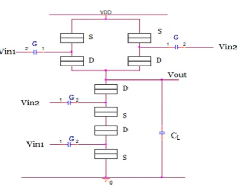
6.SINGLE ELECTRON NOR CIRCUIT
The action neither of two inputs NOR as shown in Figure can be explained as follows.
Figure 7. Illustration of two input NOR gate using SET
Here the P-SETs are in series and N-SETs are connected parallel to understand the logic function of NOR. When both inputs (Vin1 and Vin2) are LOW, the upper transistors connected to VDD is ON and the lower transistors are turned OFF. Hence at initial condition, the tunnel capacitors are charged that result in HIGH output. When any one input (Vin1 or Vin2) is low, the OFF
condition of a P-SET switch makes an open circuit.Therefore, the charge stored in load capacitance discharges to ground through the N-SET switch making the output LOW
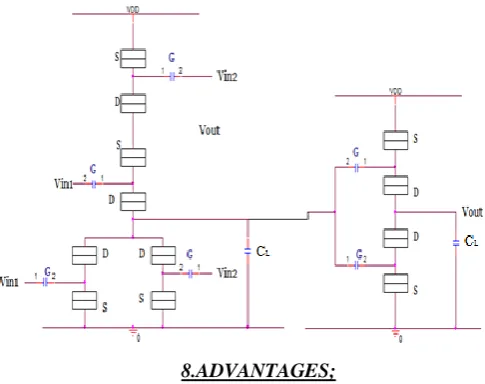
7.REALIZATION OF AND/OR CIRCUIT USING UNIVERSAL GATES
When the output of NAND and NOR gates are fed to an inverter circuit, AND gate and OR gate can be recognized respectively as shown in Figure .The operation of the device is similar to logic gates explained above. The Single Electron Transistor (SET) is a nanoscale three terminal device that provides current conduction characteristics comparable to a MOSFET and can be used for developing nanoscale logic circuits. In this paper, we have determined the design parameters of an SET to observe current oscillations at room temperature. These parameters have been used to design SET-based logic gates for room temperature operation. The circuit architectures of the proposed SET-based logic gates are identical to the corresponding CMOS gates. Complementary operations of an SET as n- and p-type devices were achieved by controlling the charge on the SET island by using the appropriate tuning gate voltages.
Figure 9 Schematic diagram of OR logic using NAND,NOR circuit respectively
8.ADVANTAGES;
1.The main benefits of the SET use are a high device integration level ultra-low power consumption.
2.The SET fabrication process is CMOS-compatible (complementary metal–oxide–semiconductor), which increases the possibilities for integrating them into complex circuits.
3.The current level of the SET can be amplified by manufacturing together with a field-effect transistor (FET), by generating a hybrid SET-FET circuit..
9.DISADVANTAGES
1. low current level
2.low temperature operation
.
10.CONCLUSIONS
SETs could be used for memory device, but even the latest SETs suffer from “offset charges”, which means that the gate voltage needed to achieve maximum current varies randomly from device to device. Such fluctuations make it impossible to build complex circuits.The future does look bright for these devices.In this context, the relevance of the SET-based circuits have been recently highlighted .There is possibility of manufacturing feasibility of the SET-FET circuits operative at room temperature. The main goal of this project is on the design of the SET manufacturability process-flow for large-scale, seeking to extend the use of the hybrid SET-CMOS architectures.
11.ACKNOWLEDGMENT
This Paper was supported by KKR AND KSR Institute Of Technology And Sciences(KITS)-Guntur-Andhra
Pradesh-India.. I thank my parents, Husband and Son who provided insight and expertise that greatly assisted the paper, although they may not agree with all of the interpretations/conclusions of this paper.
12.REFERENCES
[1] J. R. Tucker, “Complementary digital logic based on the Coulomb blockade,” J. Appl. Phys., vol. 72, no. 9, pp. 4399–4413, Nov. 1992.
[2] C. Wasshuber, Computational Single-Electronics. New York: Springer-Verlag, 2001.
[3] K. K. Likharev, “Single-electron devices and their applications,” Proc. IEEE, vol. 87, pp. 606–632, Apr. 1999. [4] C. J. Gorter, “A possible explanation of the increase of the electrical resistance of thin metal films at low temperatures and small field strengths,” Physica, vol. 17, no. 8, pp. 777–780, Aug. 1951.
[5] C. Wasshuber, H. Kosina, and S. Selberherr, “A comparative study of single-electron memories,” IEEE Trans. Electron Devices, vol. 45, pp. 2365–2371, Nov. 1998. [6] C. P. Heij, P. Hadley, and J. E. Mooij, “Single-electron inverter,” Appl. Phys. Lett., vol. 78, no. 8, pp. 1140–1142, Feb. 2001.
[7] T. Altebaeumer and H. Ahmed, “Silicon nanowires and their application in bi-directional electron pumps,” Microelectron. Eng., vol. 57–58, pp. 1029–1033, 2001. [8] H. Iwamura, M. Akazawa, and Y. Amemiya, “Single-electron majority logic circuits,” IEICE Trans. Electron., vol. E81-C, no. 1, pp. 42–46, Jan. 1998.
[9] C. R. Lageweg, S. D. Cotofana, and S. Vassiliadis, “A linear threshold gate implementation in single electron technology,” in Proc. IEEE Computer Society Workshop VLSI 2001: Emerging Technologies VLSI Systems, Orlando, FL, Apr. 2001, pp. 93–9
[10] Mahapatra, V. Vaish, C. Wasshuber, K. Banerjee, and A. M. Ionescu, "Analytical Modeling of Single Electron Transistor for Hybrid CMOS-SET Analog IC Design," IEEE Trans. Electron Devices, vol. 51, no. 11, pp. 1772–1782, Nov. 2004.
[11]Jump up^ K. Uchida, K. Matsuzawa, J. Koga, R. Ohba, S. I. Takagi, and A. Toriumi, "Analytical single-electron transistor (SET) model for design and analysis of realistic SET circuits," Jpn. J. Appl. Phys., vol. 39, no. 4 B, pp. 2321–2324, 2000.
[12]Jump up^ A. M. Ionescu, S. Mahapatra, and V. Pott, "Hybrid SETMOS Architecture With Coulomb Blockade Oscillations and High Current Drive," IEEE Electron Device Lett., vol. 25, no. 6, pp. 411–413, Jun. 2004.