522 | P a g e
LEAKAGE POWER AND AREA OPTIMIZATION IN
CMOS LOGIC DESIGN IN SUB MICRON
TECHNOLOGY
Manish Kumar Chandela
1, Prof. Laxmi Narayan Gahalod
21
M-Tech Research Scholar,
2Research Guide
Department of Electronics & Communication Engineering, LNCT, Bhopal
ABSTRACT
In VLSI circuits and systems. Due to relatively high complexity of VLSI systems used in various applications,
the power dissipation in CMOS inverter arises from its switching activity, which is mainly influenced by the
supply voltage and effective capacitance. One of challenge with technology scaling is the rapid increase in sub
threshold leakage power due to Vt reduction. Leakage power dissipation is a component of static power
dissipation in CMOS circuits. It is caused by the presence of leakage currents in the MOS transistors. Leakage
power can be reduce by Stack, Sleep and Sleepy keeper transistor techniques. Sleepy Keeper technique provided
lesser static power dissipation and lesser static power delay product in comparison with the other techniques.
The main advantage of using Sleepy Keeper technique is that it retains the logic state and also lowers the sub
threshold leakage power dissipation. It has been shown previously that the stacking of two off transistors has
significantly reduced sub-threshold leakage compared to a single off transistor. In stack transistor technique
two half channel width transistors are connected in series to for one of the transistor in pull up and pull down
networks with gates to increase the stack effect, it will increase the resistance between the supplyand ground.
Therefore, the leakage of the logic gate is reduced. A MOS transistor in the circuit is divided and stacked into
two half width size transistors. When two half size stacked MOS transistors are turned off together, induce
reverse bias between them results in the reduction of the sub thresholdleakage power. However, increase in the
number of transistors increases the overall propagation delay of the circuit.
I. INTRODUCTION
Leakage power can be reduce by Stack and Sleep transistor techniques. It has been shown previously that the
stacking of two off transistors has significantly reduced sub-threshold leakage compared to a single off
transistor. In stack transistor technique two half channel width transistors are connected in series to for one of
the
Transistor in pull up and pull down networks with gates to increase the stack effect, it will increase the
resistance between the supply and ground. Therefore, the leakage of the logic gate is reduced. A MOS transistor
in the circuit is divided and stacked into two half width size transistors. When two half size stacked MOS
523 | P a g e
leakage power. However, increase in the number of transistors increases the overall propagation delay of thecircuit.
1.1. Leakage Power Source
Sub threshold leakage current is the most dominant component of leakage current (power) in short channel
MOS transistors. This leakage current is caused by the inability to completely turn off a MOS transistor. Due to
the reversely biased pn junction the transistor conducts even in weak inversion region below the threshold
voltage of the MOS transistor.
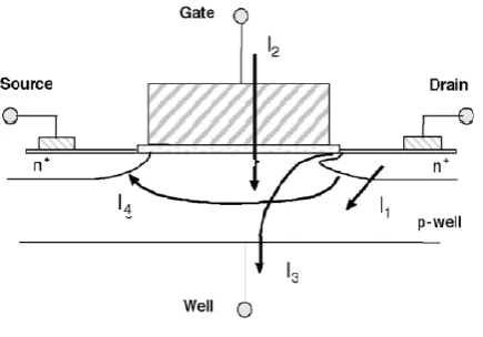
There are four main sources of leakage current in a CMOS transistor
i) Junction Leakage (I1): The junction leakage occurs from the source or drain to the substrate through the
reverse-biased diodes when a transistor is OFF. A reverse-biased pn junction leakage has two main components:
one is minority carrier diffusion/drift near the edge of the depletion region; the other is due to electron-hole pair
generation in the depletion region of the reverse-biased junction.
ii) Gate-Induced Drain Leakage (I2): The gate induced drain leakage (GIDL) is caused by high field effect in
the drain junction of MOS transistors. For an NMOS transistor with grounded gate and drain potential at VDD,
significant band bending in the drain allows electron-hole pair generation through avalanche multiplication and
band-to-band tunneling. A deep depletion condition is created since the holes are rapidly swept out to the
substrate. At the same time, electrons are collected by the drain, resulting in GIDL current.
iii) Gate Direct Tunnelling Leakage (I3): These current results from the tunnelling of electrons into the
conduction band of the oxide layer under a high applied electric field across the oxide layer. This direct
tunnelling current increases exponentially with the gate oxide thickness and supply voltage.
iv) Subthresold Leakage (I4): The sub threshold leakage is the drain-source current of a transistor i.e. channel
punch through current.
Fig 1 Leakage currents in MOSFET
Increasing the threshold voltage of a transistor reduces the leakage current exponentially, but it has a marginal
effect on the dynamic power dissipation. On the other hand, reducing the width of a transistor reduces both
leakage and dynamic power, but at a linear rate only.
1.2. Stack Technique
524 | P a g e
The stack effect, it will increase the resistance between the supply and ground. Therefore, the leakage of thelogic gate is reduced. A MOS transistor in the circuit is divided and stacked into two half width size transistors.
When two half size stacked MOS transistors are turned off together, induce reverse bias between them results in
the reduction of the sub threshold leakage power. However, increase in the number of transistors increasesthe
overall propagation delay of the circuit. When a stack of two or more transistors are turned off, the time required
for voltagesand currents to settle to quiescent levels is large and can vary over a wide range.
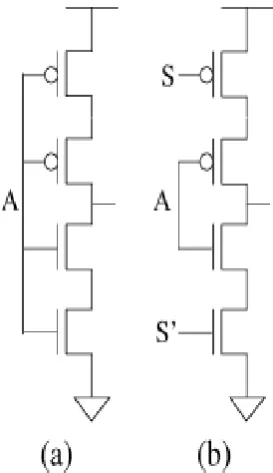
Fig 2 Stack Technique series connected half channel width MOSFET
.
Fig 3 Not logic Gate using (a) stack method
(b) Sleep transistor method.
1.3. Sleep Technique
Sleep transistors of high threshold voltages are used in the Sleep technique. A sleep pMOS transistor is placed
between the supply voltage, VDD and the pull-up network and a sleep nMOS transistor is placed between the
pull down network and the ground, GND. These sleep transistors are turned ON when the circuit is in active
state and turned OFF when the circuit is in sleep state. This technique reduces the sub threshold leakage current
525 | P a g e
transistors are driven by sleep signals. Using this technique the present state of the circuit is lost and thus resultsin destruction of the present logic state.
Fig 4. Sleep transistor technique
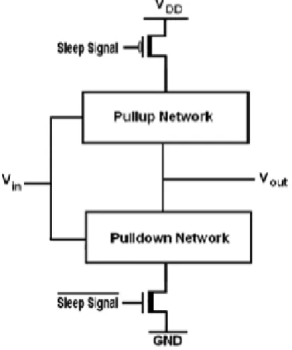
1.4. Sleepy Keeper Technique
In this technique, an additional high threshold voltage nMOS transistor is connected in parallel with the sleep
pMOS transistor and an additional high threshold voltage pMOS transistor is connected in parallel with the
sleep nMOS transistor. In sleep mode, the sleep transistors are in cut-off state. So, when sleep signal is
activated, then the high threshold voltage nMOS transistor connected in parallel
With the sleep pMOS transistor is the only source of power supply to the pull-up network and the high threshold
voltage pMOS transistor connected in parallel with the sleep nMOS transistor provides the path to connect the
pull down network with ground. The major advantage in using Sleepy keeper technique is that it reduces the
significant sub threshold leakage current and also retains the circuit present state in sleep mode.
526 | P a g e
In stack transistor technique two half channel width transistors are connected in series to for one of the transistorin pull up and pull down networks with gates to increase the stack effect, it will increase the resistance between
the supply and ground. Therefore, the leakage of the logic gate is reduced. A MOS transistor in the circuit is
divided and stacked into two half width size transistors. When two half size stacked MOS transistors are turned
off together, induce reverse bias between them results in the reduction of the sub threshold leakage power.
However, increase in the number of transistors increases the overall propagation delay of the circuit.
II. THRESHOLD VOLTAGE VARIATION DUE TO SUBSTRATE BIAS EFFECT
It shows that the threshold voltage of the characteristics does not change very much as the body is
reverse-biased, while it becomes lower as the body is forward-biased. The threshold voltage becomes higher as the body
is reverse-biased and stops rising when the body bias exceeds a certain value, while the threshold voltage
becomes lower as the body is forward-biased. It also shows the dependence on the channel impurity
concentration, drain voltage, and gate length. It is clear that a higher impurity concentration requires a higher
body-bias to reach a constant threshold voltage. The higher drain bias and a shorter gate length decrease the
body bias for the threshold voltage saturation. We think that this is because it is easy for the body region near
the drain edge to become fully depleted by the drain bias and this affects all the characteristics of the
short-channel device.
III. POWER DISSIPATION
Power dissipation in VLSI circuits can be broadly divided into two categories: Dynamic or switching power,
and Static or leakagepower dissipations
.
Dynamic power dissipation results due to charging and discharging ofinternal capacitances in the circuit. Leakage power dissipation occurs during the static input state of the device.
Leakage power dissipation is much more noticeable in low threshold voltage MOS transistors. This power
dissipation arises because of the presence of sub threshold and gate oxide leakage currents. Subthershold
leakage current flowing through a stack of series-connected transistors reduces when more than one transistor in
the stack is turned off. The phenomenon whereby the leakage current through a stack of two or more OFF
transistors is significantly smaller than a single device leakage is called the ―stack effect‖. In both cases a
transistor is added in series with one of the N or P networks. It will increase the resistance between the supply
and ground. This decreases the gate leakage because of the transistor stack effect. Here we can design the full
adder logic circuit using stack transistor technique.
IV. Literature Survey
Related Work:
Niranjan Kulkarni, Jinghua Yang, Jae-Sun Seo, and SarmaVrudhula "Reducing Power, Leakage, and Area of
Standard-Cell ASICs Using Threshold Logic Flip-Flops" IEEE Transactions On Very Large Scale Integration
(Vlsi) Systems, Vol. 24, No. 9, September 2016 pp no. 2873.
In this work author describe a new approach to reduce dynamic power, leakage, and area of
application-specified integrated circuits using a combination of conventional logic gates and threshold logic flip-flops,
527 | P a g e
seamless integration with conventional standard-cell design flow. We first describe a new robust, standard-celllibrary of configurable circuits for implementing threshold functions. Abstractly, the threshold gate behaves as a
multi-input, singleoutput, edge-triggered flip-flop, which computes a threshold function of the inputs on the
clock edge. The library consists of a small number of cells, each of which can compute a set of complex
threshold functions, which would otherwise require amultilevel network. The function realized by a given
threshold gate is determined by how signals are mapped to its inputs.
Ing-Chao Lin, Kuan-Hui Li, Chia-Hao Lin, and Kai-Chiang Wu publish there work on title "NBTI and Leakage
Reduction Using ILP-Based Approach" in IEEE Transactions On Very Large Scale Integration (Vlsi) Systems,
Vol. 22, No. 9, SEPTEMBER 2014. They use the transmission gate and gate replacemnment technique to
reduce the leakage power. In there technique, it adds a TG and a pull-up transistor in front of the gate that needs
protection with original circuit. Gates G1 and G2 are on the critical path, whereas G3 is not. During the standby
mode, the output value of G1 is zero, causing stress on G2 and increasing the delay. To reduce NBTI, a TG and
a pulluppMOS transistor are inserted after G1. The value after TG becomes one when the sleep signal is one,
reducing the NBTI degradation. Simultaneously, gate G3 connects to the G1’s output, which has a signal of
zero, reducing leakage power.
Fabio Frustaci, Pasquale Corsonello, and StefaniaPerri publish their work on title "Analytical Delay Model
Considering Variability Effects in Subthreshold Domain" in IEEE Transactions On Circuits And Systems—Ii:
Express Briefs, Vol. 59, No. 3, March 2012 pp no. 168 [1]. They propose a delay models which take the effects
of the process variability and of the transient variation of the transistors’ on-current during the switching into
account.CMOS technology scaling enhances the computing capability of integrated circuits. Increasing numbers
of miniaturized transistors are crammed onto integrated circuits, thereby enhancing the functionality.
Furthermore, the operating frequency of integrated circuits increases with each new technology generation. This
technology creates parasitic elements in the integrated chip which may degrade the performance of devices.
Owing to this, delays are predicted with accuracy significantly higher than existing accurate delay models.
Furthermore, the novel models are also suitable for gateswith transistors’ stacks. They use of the proposed two
NAND gate models with transistor stacks of the propagation delay of CMOS circuits in the sub threshold
domain. The first model refers to the CMOS inverter, whereas the second one is usable for all gates with
transistors stacks. Both models take into account the transient variation of Ion during the switching activity and
the effects due to pr
o
cess variations. This represents a significant novelty with respect to the existing delaymodels that treat a stack as a single transistor with an equivalent width
[1].
Changing the substrate voltagecauses the threshold voltage to change. So the different kind of effect is arises for changing the substrate voltage
like Zero-Body Bias, Reverse-Body Bias and Forward-Body Bias. This Phenomenon is frequently used for
controlling the threshold voltage. Constant dependent on the transistor parameter and the technology feature
size. By controlling body biasing effect with changing the constant term we can easily control the leakage
power.
J. P. Campbell, Member, K. P. Cheung, J. S. Suehle, and A. Oates publish their work
on title
"A Simple SeriesResistance ExtractionMethodology for Advanced CMOS Devices in " IEEE Electron Device Letters, Vol. 32,
528 | P a g e
derived only from the ratio of two linear ID–VG measurements. This approach has a verifiable accuracy checkand is successfully used to extract the series resistance from several advanced devices. Furthermore, the validity
of the assumptions used in this series resistance extraction procedure is examined and shown to be justified.
Parasitic resistance such as channel resistance (Rchannel), series resistance (RSD) has become a serious obstacle
inhibiting the performance of CMOS devices. As channel length scaling continues to reduce the channel
resistance (Rchannel), series resistance (RSD) is becoming a larger fraction of the total device resistance (RTotal=
RSD + Rchannel) and is soon expected to limit the performance in advanced devices. The on-state resistance of a
MOSFET is made up of several components. The propagation delay of the network excited by the step function
is proportional to the time constant of the network. In this case time constant is the product of the resistor and
load capacitor.
V. PROBLEM FORMULATION
1 .Sub threshold con reduces by stack transistor technique which operates when circuit is in standby mode. The
stack transistors are design by two series connected half size transistors.
2. We will do the parametric analysis on delay, number of transistors and sub threshold power dissipation.
3. The static and dynamic power of stack is considerably low. But it has a delay penalty and its area requirement
is maximum compared with other processes. This can be overcome by using stack transistors of half size.
4. Our goal is to trade off between these limitations and thus propose new methods which reduce both leakage
and dynamic power with minimum possible area and delay trade off.
5. A MOS transistor in the circuit is divided and stacked into two half width size transistors. When two half size
stacked MOS transistors are turned off together, induce reverse bias between them results in the reduction of the
sub threshold leakage power. However, increase in the number of transistors increases the overall propagation
delay of the circuit.
VI. CONCLUSION
This paper discusses the static power dissipation sources in MOSFET and its reduction techniques.This work
reviewed circuit optimization design techniques for controlling the OFF current of CMOS circuits in both
standby and active modes of circuit operation. The sub threshold leakage control techniques that do not
adversely affect the circuit performance and layout cost. This is especially important in light of both statistical
process parameter variations
and
their impact on leakage currents. The stacking of two off devices hassignificantly reduced sub-threshold leakage compared to a single offdevice. Logic gates after stack forcing will
reduce leakage power, but incur a delay penalty, similar to replacing a low- Vt device with a high-Vt device in a
dual-Vt design.
REFERENCES
[1] Niranjan Kulkarni, Member, IEEE, Jinghua Yang, Member, IEEE, Jae-Sun Seo, Member, IEEE, and Sarma
Vrudhula "Reducing Power, Leakage, and Area of Standard-Cell ASICs Using Threshold Logic Flip-Flops"
529 | P a g e
[2] Ing-Chao Lin, Chin-Hong Lin, and Kuan-Hui Li "Leakage and Aging Optimization Using TransmissionGate-Based Technique" IEEE Transactions On Computer-Aided Design Of Integrated Circuits And Systems,
Vol. 32, No. 1, January 2013 pp no. 87.
[3] Mathieu Luisier and Olaf Schenk "Gate-Stack Engineering in n-Type Ultrascaled Si Nanowire Field-Effect
Transistors" IEEE Transactions On Electron Devices, Vol. 60, No. 10, October 2013 pp no. 3325.
[4] Yu Wang,Xiaoming Chen, Wenping Wang,Yu Cao, Yuan Xie, and Huazhong Yang "Leakage Power and
Circuit Aging Co optimization by Gate Replacement Techniques" IEEE Transactions On Very Large Scale
Integration (Vlsi) Systems, Vol. 19, No. 4, April 2011.
[5] Ing-Chao Lin, Kuan-Hui Li, Chia-Hao Lin, and Kai-Chiang Wu "NBTI and Leakage Reduction Using
ILP-Based Approach" IEEE Transactions On Very Large Scale Integration (Vlsi) Systems, Vol. 22, No. 9,
September 2014 pp no. 2034.
[6] Hailong Jiao and VolkanKursun "Threshold Voltage Tuning for Faster Activation With Lower Noise in
Tri-Mode MTCMOS Circuits" IEEE Transactions On Very Large Scale Integration (Vlsi) Systems, Vol. 20, No.
4, April 2012 pp no. 741.
[7] AshokaSathanur, Luca Benini, Alberto Macii, Enrico Macii, and Massimo Poncino "Row-Based
Power-Gating: A Novel Sleep Transistor Insertion Methodology for Leakage Power Optimization in Nanometer
CMOS Circuits" IEEE Transactions On Very Large Scale Integration (Vlsi) Systems, Vol. 19, No. 3, March
2011 pp no. 469.
[8] RakeshGnana David Jeyasingh, NavakantaBhat, and BharadwajAmrutur "adaptive Keeper Design for
Dynamic Logic Circuits Using Rate Sensing Technique" IEEE Transactions On Very Large Scale
Integration (Vlsi) Systems, Vol. 19, No. 2, February 2011 pp no. 295.
[9] YolinLih, Member, IEEE, NestorasTzartzanis, Member, IEEE, and William W. Walker "A Leakage Current
Replica Keeper for Dynamic Circuits" IEEE Journal Of Solid-State Circuits, Vol. 42, No. 1, January 2007 pp
no. 48.
[10] QianXie, Jun Xu, and Yuan Taur "Review and Critique of Analytic Models of MOSFET Short-Channel