1 |
P a g e
LOW-POWER 1-BIT FULL-ADDER CELL USING
ENHANCED PASS TRANSISTOR LOGIC AND POWER
GATING
1T.S.Ananth,
2A.Vijay,
3Dr.G.K.D.Prasanna Venkatesan
123
PGP College of Engineering and Technology, Namakkal, Tamilnadu (India)
ABSTRACT
Adders have become one of the important components in the digital world, such that there exists no design
without it. Adders are not only used for additions, but it is also one of the basic building blocks that have been
used for many other functions such as subtractions, multiplications, and divisions etc.
In the field of Very Large Scale Integration (VLSI), Adders are used as the basic component from processors to
ASICs. Propagation delay, Power and Area are the acceptable Quality metrics of the designed products. Recent
days has proved that the use of Complementary Pass Transistor Logic (CPL) and sleep transistor provides a
drastic reduction in the power compared to CMOS logic. Power Gating is one such well known technique where
a sleep transistor is added between actual ground rail and circuit ground. The device is turned off during sleep
mode to cut-off the leakage path. This technique results in a substantial reduction in leakage at a minimal
impact on performance. This paper has spread the focus on Low power Adder design based on PTLs, with
reduced sub threshold leakage power consumption and ground bounce noise during sleep to active mode
transition, thereby achieving 2.5% reduction in power without affecting other quality metrics of the design. The
CPL design has been modeled and analyzed using TANNER EDA with TSMC MOSIS 250nm technology. In the
present paper we will propose low leakage 1 bit CMOS full adder circuit in 90nm technology with supply
voltage of 1V.
Keywords: CPL, Power, VLSI, Adder
1. INTRODUCTION
The demands of the VLSI Industry can be addressed at various stratus of design such as design level,
architectural, circuit and process technology level. Selecting the appropriate style holds the key for design and
implementation of power efficient circuit systems. The switching capacitance, short circuit current, and the
transition activity hold a considerable influence on the power consumption.
Each of these parameters plays a vital role depending on the technique used in the circuit for the application.
The technological market today with vast applications along with inflow of multimedia devices has promoted
the Low power design as a major need for the modern world. A couple of decade before, the demands of the
industry was speed, reduction in size or its capacity to handle more components per unit area and low cost.
Hence most of the scientific communities focus on Low power design techniques. The reliability of most the
2 |
P a g e
CMOS circuit due to 1) switching power 2) short circuit power 3) static power. The switching power is causeddue to charging and discharging of capacitance. The short circuit power loss is caused due to power flow from
power supply to ground with simultaneous functioning of p-network and n-networks. The leakage current causes
loss in static power.
Literature review in the last decade has revealed some of the adder designs using different logic styles. In [1]
Kang has proposed an adder design with pull-down and pull-up network using 28 transistors [3]. Full Adder
using XOR/XNOR PTL cell with 16 transistors is reported in [4]. 32-Transistor Complementary pass-transistor
logic (CPL) with high power dissipation and better driving capability was proposed in [5]. Full adder design
with 10 transistors using XOR/XNOR gates is also reported in [6]. A hybrid CMOS logic style adder with 22
transistors is reported in [7].
2. ARCHITECTURE OF FULL ADDER
A basic full adder has three inputs and two outputs which are sum and carry. Full adder cell is designed with
CPL and Multiplexing Control Input technique for both sum and carry operations. The Sum and Carry
operations are based on the equations 1 & 2 mentioned below:
Sum = A⊕ B⊕ C (1)
Carry = (A⊕ B)C + AB (2)
Sum equation contains XOR gates whose design using CPL logic is desired for low power system, whereas the
Carry is designed as per equation.
Fig 1: Full Adder Circuit [9]
The inputs A, A's complement (A'), B, and B's complement (B') are fed to the pass transistors and forms an XOR
logic gate. These four inputs construct an XOR logic operation at the transistor level, which is designed using
two transistors. To reduce the number of transistors, the output of the XOR gate (A⊕ B) is fed through a NOT
gate from the differential node to the pass transistors as a control input. Whereas, Cin is treated as variable
3 |
P a g e
At this point, the functionality performed by the circuit is equivalent to the sum operation, sum A⊕B⊕C, and sixtransistors have been used. As mentioned earlier, the number of transistors in the carry operation can be reduced
by taking A⊕ B as the input from the sum operation circuit AND with Cin in order to produce the operation
equivalent to (A⊕ B)Cin, which only uses another two transistors. Meanwhile, the inputs A, A', B, and B' are
fed into pass transistors in order to produce an AND logic gate, that represents the AB operation in Equation (2).
The outputs of both (A⊕ B) C and AB are used as multiplexing inputs to sum both terms with the OR gate
operation. By modifying the OR gate at the last stage of the carry equation, the transistor count can be further
reduced.
This enhancement can be performed by removing the inverter and the transistor fed by the inverter. Markovic’s
[8] full adder circuit has 22 transistors. Earlier, 3 transistors were omitted in our design and the number of
transistors of the full adder cell was reduced to 17 transistors, which is much lower than the number of
transistors in the circuit 22 transistors described by Markovic [8]. Fig 1 shows the full adder circuit using 17
transistors [9]. And Fig 2 shows the proposed full adder circuit for power optimization.
Fig 2: The proposed Full Adder circuit
The proposed low power full adder consists of both PMOS & NMOS transistors. The focus is to eliminate the
power hungry inverters. The NMOS transistors that require inversion of gate input are replaced by PMOS
transistors.
3. SIMULATION AND PERFORMANCE ANALYSIS OF A FULL ADDER
The existing & proposed architectures are implemented using Full Custom ASIC design methodologies. Both
the existing & proposed full adder architectures are simulated using Tanner tool which are mapped to TSMC
250 nm technology node.
Table I shows the benchmarking results of the existing & proposed architectures after implementing using this
ASIC design methodology. As depicted in Table I the proposed architecture is well suitable for area optimized
applications and the performance of the proposed architecture is also unaffected. From Table I, it is clear that the
4 |
P a g e
is significant to note that the power is reduced. Since this change occurs in the architectural design of the device,below are the advantages of low power:
No area or performance penalty Minimum verification effort High scalability
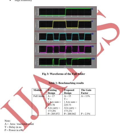
Fig 3: Waveforms of the Full Adder
Table 1: Benchmarking results
Module Existing
Design
Proposed Design
The Gain Factor Full Adder A = 17
T = { A to sum = 225.78 A to carry = 173.28} P= 205.072
A = 15 T = { A to sum = 225.73 A to carry = 173.23} P= 200.042
A = 11%
P = 2.5%
Note:
A = Area / transistor count T = Delay in ns
P = Power in nW
4. POWER REDUCTION USING GATING TRANSISTOR
The power reduction must be achieved without comprising performance which makes it hard to reduce leakage
current during normal operation of mobile. We perform analysis and simulation of various parameters such as
standby leakage power, active power, ground bounce noise and propagation delay using Cadence Spectre 90nm
5 |
P a g e
Implementation of adder cells to reduce power consumption and to increase the speed has proved as an efficientsolution for power reduction. Moreover, realization of adders with different approaches using CMOS technology
widens the area of power reduction [1], [2]. Performance of the adder cells can be evaluated by measuring the
factors such as leakage power, active power, ground bounce noise in context to voltage and transistor scaling.
The power gating technique uses high threshold voltage sleep transistor which cut-off a circuit block when the
block is not switching [9]. Here the sleep transistor is connected between actual ground rail and virtual ground
[6], [7]. This insertion of sleep transistor divides the power network into a permanent power network connected
to the power supply and a virtual power network that drives the cells and can be turned off during inactive
period. The sizing of sleep transistor is an important design factor. This technique is also known as MTCMOS or
Multi-Threshold CMOS and reduces standby or leakage power.
Power gating affects design architecture more than clock gating. It increases time delays as power gated modes
have to be safely entered and exited. Architectural trade-offs exist between designing for the amount of leakage
power saving in low power modes and the energy dissipation to enter and exit the low power modes. Shutting
down the blocks can be achieved either by software or hardware. Power gating uses low-leakage PMOS or
NMOS as sleep transistors.
As told earlier, the CMOS circuit is the base adder and all simulation results comparison has been done with it.
It consists of 28 transistors incorporating PMOS pull up and NMOS pull down networks to produce desired
outputs. Here the sizing of transistors plays a vital role. Here, the transistor ratio of PMOS to NMOS has been
kept 2 for an inverter and on considering the remaining blocks as equivalent inverters also follows the same
ratios. When it is simulated in 90nm process, it provided very poor results in context to leakage power. Thus the
adder circuit was modified with proper sizing using power gating technique.
The power gating technique is shown to reduce the leakage power by placing a sleep transistor between actual
ground rail and circuit ground (virtual ground). Here low leakage NMOS is used as a sleep transistor. Estimation
of the ground bounce noise is done when circuit is connected to the sleep transistor.
The width and length of smallest transistor has been kept 120nm and 100nm respectively for 90nm CMOS
technology. The W/L ratio for NMOS is kept as 1.2 whereas for PMOS its 3.8 which are 3.1 times that of
NMOS in Fig.1. The sizing of each block is based on the assumptions that each block is equivalent to inverter
and same inverter ratio is maintained for each block. Since sub threshold current is directly proportional to W/L
ratio of transistor, the sizing reduces the standby leakage current to a very great extent.
5. ACTIVE POWER AND STANDBY LEAKAGE POWER
The dissipation of power which occurs during the active mode of the circuit is active power. This active power
consists of dynamic power as well as the static power. It is measured by giving input vectors to the circuit, then
calculating the average power dissipation and comparing the result with the base adder i.e. conventional 1-bit CMOS
6 |
P a g e
Ground Bounce is the voltage oscillation between ground pin on a component package and the ground reference levelon the component die. Essentially it is caused by a current surge passing through the lead inductance of the package.
The effect is most visible when all outputs switch simultaneously. In saturation region an instantaneous charge current
passes through the sleep transistor, during power mode transition.
6. PERFORMANCE ANALYSIS AND SIMULATED RESULTS
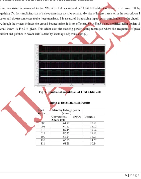
Sleep transistor is connected to the NMOS pull down network of 1 bit full adder circuit and it is turned off by
applying 0V. For simplicity, size of a sleep transistor must be equal to the size of largest transistor in the network (pull
up or pull-down) connected to the sleep transistor. It is measured by applying input vector combinations to the circuit.
Although the system reduces the ground bounce noise, it is not efficient. So in Fig.5 a new modified adder design of
what shown in Fig.2 is given. This adder uses the stacking power gating technique where the magnitude of peak
current and glitches in power rails is done by stacking sleep transistors [9].
Fig 4: Functional simulation of 1-bit adder cell
Table 2: Benchmarking results
Input Vector
Standby leakage power (n watt)
Conventional CMOS
Adder Cell
Design 1
000 64.72 13.21
001 69.62 14.92
010 87.45 17.24
011 86.32 19.41
100 63.24 18.71
110 66.55 14.67
7 |
P a g e
Fig 5: Functional simulation of 1-bit adder cell with sleep transistor
7. CONCLUSION
The proposed full adder cell has been simulated and results are compared with existing full adder cell in terms of area
and power. This proposed adder cell is having improvement in both of these aspects. The proposed low power concept
is proven in both ASIC Design Methodologies.
The 1-bit full adder cell with power gating technique is implemented where a sleep transistor is added between actual ground rail and circuit ground. The device is turned off during sleep mode to cut-off the leakage path. For optimal performance, stacking power gating technique has been implemented where SELECT input to stacked sleep transistor with delta T delay further reduces the leakage power and ground bounce noise.
The comparison of active power, standby leakage power is done and it is observed that power consumption is greatly reduced as we navigate from conventional CMOS full adder cell to Modified Design2. The ground bounce noise is compared for Modified Design2 without delay and with delay and it is reduced in the later case. The implemented 1-bit full adders are designed using 90nm technology and operated supply voltage of 1V.
REFERENCES
[1] Chandrakasan, A., Brodersen,“Low Power Digital Design”, Kluwer Academic Publishers, R., 1995. [2] N. Weste and K. Eshraghian, “CMOS VLSI Design- A Circuits & System Perspective”, Pearson Education,
2008.
[3] Y. Leblebici, S.M. Kang, CMOS Digital Integrated Circuits, Singapore: Mc Graw Hill, 2nd edition, 1999. [4] A. M. Shams and M. Bayoumi, “A novel high-performance CMOS1- bit full adder cell,” IEEE Transaction
on Circuits Systems II, Analog Digital Signal Process, vol. 47, no. 5, pp. 478–481, May 2000.
[5] R. Zimmermann, and W. Fichtner, “Low-power logic styles: CMOS versus pass-transistor logic,” IEEE J. Solid
State Circuits, vol. 32, no. 7, pp. 1079-1090, Jul. 1997.
[6] H. T. Bui, Y. Wang, and Y. Jiang, “Design and analysis of low-power 10-transistor full adders using XOR-XNOR gates,” IEEE Transactions Circuits Systems II, Analog Digital Signal Process, vol. 49, no. 1, pp. 25– 30, Jan. 2002.
[7] S. Goel. A. Kumar, M. A. Bayoumi, “Design of robust, energy – efficient full adders for deep sub micrometer design using hybrid- CMOS logic style” IEEE Transactions on Very Large Scale Integration (VLSI) Systems, vol.14, no.12, pp.1309-1321, Dec. 2006.
[8] D Markovic, B Nikolic, and V G Oklobdzija, "A general method in synthesis of pass-transistor circuits," Microelectr. J, vol. 31, pp. 991-8, 2000.
8 |
P a g e
[10] C Senthilpari, “A Low-power and High-performance Radix-4 Multiplier Design Using a Modified Pass-transistor Logic Technique” IETE Journal of Research, Vol: 57, Issue No.: 2, Page: 149-155, May 2011. [11] K. Kawasaki et al., “A sub-us wake-up time power gating technique with bypass power line for rush current
![Fig 1: Full Adder Circuit [9]](https://thumb-us.123doks.com/thumbv2/123dok_us/9165293.1455121/2.595.70.519.158.640/fig-full-adder-circuit.webp)