Ratansang S Vaghela¹ and Priyesh P. Ghandhi²
1,2
Electronics and Communication Dept, LCIT, Bhandu, North Gujarat, India Abstract ___ This paper contain a low voltage, low offset and high speed proposed cmos voltage comparator. It has application in mainly flash and pipeline ADC. It has been characterized with features like propagation delay, offset voltage, input common mode range, slew rate and speed etc. Simulation is done with the help of mentor graphics using TSMC 180nm and Generic 90nm technology. Comparative analysis of proposed comparator with previous dynamic Comparator using both technologies has been shown.
Keywords__ Dynamic latch comparator; proposed comparator; low offset; low power: high speed; ADC etc.
I. INTRODUCTION
Due to low-offset, fast speed, low power consumption, high input impedance, CMOS dynamic latched comparators are very attractive for many applications such as high speed analog-to-digital convertors(ADCs), memory sense amplifiers(SAs) and data receivers. They use positive feedback mechanism with one pair of back-to-back cross coupled inverters for converting a small input-voltage difference to a full-scale digital level in a short time.[01] However, an input-referred latch offset voltage, due to static mismatches such as threshold voltage Vth and ß variations in the regenerative latch, degrade the accuracy of such comparators. Moreover, dynamic mismatch from the unbalanced parasitic capacitances on the output nodes of the latch causes the additional offset term during evaluation phase. So, the input-referred latch offset voltage is one of the most important design parameters of the latched comparator. By using large device sizes for the latching stage, a low offset can be achieved at the cost of the reduced speed due to slowing the regeneration time and the increased power dissipation. In this paper we are going to implement the some pair of transistors of latch stage connected in parallel for offset voltage reduction in double tail comparator due to mismatch in transistor pairs. This technique called Differential spit level logic (DSLL) which uses the latch as load in the first stage is used to reduce offset voltage in the second stage. Fast speed and low power consumption are the two most important parameter of the comparator which is to be used in high speed ADCs. [3] This paper is organized as follow. Section II, describe as Convectional dynamic comparator. Section III introduced differential comparator. Section IV proposed comparator and Section V consist of simulation results of three comparators. In section V table comparison for characteristics like propagation delay, offset voltage, ICMR, slew rate and speed. Conclusion and references are illustrated in section VI.
II. CONVECTIONAL DYNAMIC COMPARATOR
This is basic circuit for understanding dynamic comparator. This comparator operates in two modes. When CLK=0. Called reset phase the transistor Mtail will be off. The transistors M5 and M6
which are called reset transistors becomes on and makes the output nodes “outp” and „outn‟ to turn into level VDD for beginning of a start condition. When CLK = VDD. Called evaluation mode then the M5 and M6 transistors are off, and Mtail becomes on then the output voltages (outp and outn), which where at VDD start to fall with different rates based on the corresponding discharging rates. Assume the case where the voltage VINP is greater than VINN then the voltage at output node discharges faster than the voltage at Outn node. As the voltage at Outp node which is discharged by M2 transistor drain current then voltage goes down to VDD-Vthp before the voltage at Outn node which is discharged by M1 transistor drain current, accordingly M7 transistor becomes on. Thus, the back to back inverters start the latch generation and the voltage at outn node becomes VDD and the voltage level at out node falls down to ground.[03]This structure has the advantages of high input impedance, rail-to-rail output swing, no static power consumption, and good robustness against noise and mismatch [1]. Due to the fact that parasitic capacitances of input transistors do not directly affect the switching speed of the output nodes, it is possible to design large input transistors to minimize the offset. The disadvantage, on the other hand, is the fact that due to several stacked transistors, a sufficiently high supply voltage is needed for a proper delay time. The reason is that, at the beginning of the decision, only transistors M3 and M4 of the latch contribute to the positive feedback until the voltage level of one output node has dropped below a level small enough to turn on transistors M5 or M6 to start complete regeneration. At a low supply voltage, this voltage drop only contributes a small gate-source voltage for transistors M3 and M4, where the gate source voltage of M5 and M6 is also small; thus, the delay time of the latch becomes large due to lower transconductances. Another important drawback of this structure is that there is only one current path, via tail transistor Mtail, which defines the current for both the differential amplifier and the latch (the cross-coupled inverters). While one would like a small tail current to keep the differential pair in weak inversion and obtain a long integration interval and a better Gm/I ratio, a large tail current would be desirable to enable fast regeneration in the latch. Besides, as far as Mtail operates mostly in triode region, the tail current depends on input common-mode voltage, which is not favorable for regeneration. [02]
III. DIFFERENTIAL PAIR COMPARATOR
Fig.2. Differential pair Comparator [04]
be pulled to Vss quickly at the regeneration moment. This ensures the input can be as low as one threshold voltage and so, a larger input swing can be achieved. The operation of comparator is as follows. When comparator is reset there is no current from VDD to VSS. The nodes of Vp and Vn are pulled to VDD-Vth. When Vlatch is VDD the sources of Differential pairs are pulled to VSS by switch M5 while drain current of differential pair are still in range of VDD-Vth voltage range because no transit current from VDD to VSS. So transistors M1-M4 are in saturation region at this moment. In mean time comparator begin to compare input voltage and reference voltage. The ratio of size between input transistor and reference transistor determine Trip point. It can be derived as
Where WA=W2=W3 WB=W1=W4
Vin =Vin+ - Vin- Vref =Vref+ -V
ref-The changes made from above circuit fig.2 for simulation is shown in below fig.3. is used. Vlatch shown between Vp and Vn is removed, secondly only Vlatch positive logic taken for clock. So, during reset pmos become on and during when Vlatch is VDD nmos comes into saturation region.
Fig.3. Differential Comparator [04]
IV. PROPOSED DYNAMIC COMPARATOR
This circuit has concept of differential Split-Level Logic (DSLL).It is a scheme where in the load is used to reduce output voltage swing and thus lower gate delays at the cost of smaller noise margins. The basic idea is shown in Fig.4.
The reference voltage is set to VDD/2 + Vth. This has the effect of limiting the output voltage
swing to a maximum of VDD and a minimum of VDD/2. The main drawback of this logic implementation is the increased power dissipation resulting from the continuous power draw through the output leg at a voltage of VDDI2. The output leg at VDD draws no DC power. In proposed comparator we made three changes from above dynamic comparators. First use of single clock. Secondly, reduction of two nmos in differential amplifier by using DSLL and two pmos reduction by using single clock. Thirdly use of single reference voltage =VDD/2+Vth. [01]
Fig.5.Proposed Dynamic Comparator
V. SIMULATION AND RESULT
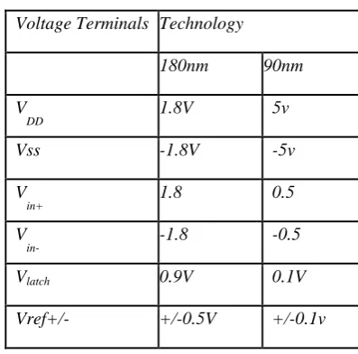
(1) The performance of the proposed dynamic comparator is compared with the other comparators for TSMC 180nm and 90nm Generic CMOS technologies shown in Table I. The supply voltage is 0.5V and a signal swing is 0.5Vpp for 90nm, differ with reference voltage of +/-0.1V shown in Table I.
(2) Simulation results for Convectional dynamic comparator, Differential pair comparator and Proposed comparator are shown in Fig.5 to Fig.12. For various characteristics like Propagation delay offset voltage, ICMR and Transit analysis using generic 90nm Technology.
(3) Comparative Analysis of Three comparators for 180nm and 90nm technologies are shown in Table no.2.A & 2.B
Table no.1 Voltage level used for simulation.
Voltage Terminals Technology
180nm 90nm
V
DD
1.8V 5v
Vss -1.8V -5v
V
in+ 1.8 0.5
V
in- -1.8 -0.5
Vlatch 0.9V 0.1V
Table no.2.A Comparative Analysis of above circuits for 90nm
Parameter
Convectional dynamic Comparator
Differential Comparator
Proposed Comparator
90 nm 90 nm 90 nm
Propagation
Delay (ns) 457ps 877ps 203ps
ICMR 499mV to -432mV 44.96mv to -499mv 499mv to -121
Offset
Voltage(mV) 144.36 mV -20.43mV -250mv
Slew rate 37V/ns 18V/ns 16V/ns
Speed 218MHz 120 MHz 492MHz
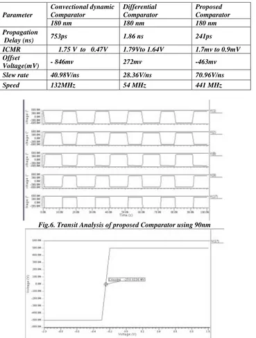
Table no.2.B Comparative Analysis of above circuits for 180nm
Parameter
Convectional dynamic Comparator
Differential Comparator
Proposed Comparator
180 nm 180 nm 180 nm
Propagation
Delay (ns) 753ps 1.86 ns 241ps
ICMR 1.75 V to 0.47V 1.79Vto 1.64V 1.7mv to 0.9mV
Offset
Voltage(mV) - 846mv 272mv -463mv
Slew rate 40.98V/ns 28.36V/ns 70.96V/ns
Speed 132MHz 54 MHz 441 MHz
Fig.6. Transit Analysis of proposed Comparator using 90nm
Fig.8.ICMR of proposed comparator using 90nm
Fig.9.Transit analysis of differential comparator using 90nm
Fig.10. Offset of differential comparator using 90nm.
Fig.11.Transist Analysis of Convectional dynamic comparator using 90nm
Fig.12.Offset and ICMR of Convectional dynamic comparators using 90nm
VI. CONCLUSION
We conclude that with reduction of technology and by using proper logic optimizing circuit can be obtained which have low power, low offset and high speed cmos voltage comparator. From comparative analysis we found that results of 90nm are better compare to 180nm technology. Also, my proposed comparators have better result compare to other two dynamic comparators.
REFERENCES
[1]R . Jacob Baker1, Harry W. Li2, David E. Boyce3, “CMOS Circuit Design, Layout and Simulation,” IEEE Press Series on Microelectronic Systems, 1997, pp.719-752.
[2]Samaneh Babayan-Mashhadi 1, Reza Lotfi 2 “Analysis and Design of a Low-Voltage Low-Power Double-Tail Comparator-2014” from Iran and Members of IEEE.
[3]Madhumathis 1, Ramesh Kumar 𝟐 “Design And Analysis Of Low Power And High Speed Double
TailComparator”M.E
[4]Student, Assistant Professor,Department Department of ECE,K.S.R College
Engineering,Tiruchengode,Tamilnadu,India
![Fig.2. Differential pair Comparator [04]](https://thumb-us.123doks.com/thumbv2/123dok_us/8362859.1672181/2.595.191.399.465.650/fig-differential-pair-comparator.webp)