Nanostructured CrAlN Films Prepared at Different Pulse Widths
by Pulsed DC Reactive Sputtering in Facing Target Type System
Sara Khamseh
1;*, Masateru Nose
2, Shohei Ueda
1, Tokimasa Kawabata
1,
Takekazu Nagae
2, Kenji Matsuda
1and Susumu Ikeno
11Department of Materials Science and Engineering, Faculty of Engineering, University of Toyama, Toyama 930-8555, Japan 2Faculty of Art and Design, University of Toyama, Takaoka 933-8588, Japan
CrAlN films have been prepared using a pulsed DC reactive sputtering in FTS system with Cr/Al alloy (¼50=50at%) targets in a mixed atmosphere of Ar and N2. The effects of pulse width on the film structure and properties have been investigated. XRD analyses were carried out to determine the phases and texture of the films. Transmission electron microscopy studies were carried out for selected films. In order to investigate the relationship between the mechanical properties and microstructure of the films, the hardness was measured by a nanoindentation system. Films prepared at lower pulse widths, exhibited fcc-CrN structure. In contrast, films that were prepared at higher pulse widths showed a mixed structure of hcp-AlN, hcp-Cr2N and a small amount of fcc-CrN phases. Plastic hardness,Hpl, of the films ranged between 32 to 41 GPa
while the Young’s modulus,EIT, of the films ranged from 320 to 340 GPa. Increasing the pulse width also resulted in an increase in the film’s
internal stress. In addition, the grain size of the samples decreased with increasing pulse width.
Consequently, the film deposited at higher pulse width exhibited high hardness of 41 GPa,H3=E2ratio of0:6and relatively lower internal stress of3:5Gpa. These results indicated that changing the pulse width can strongly affect structure and properties of CrAlN films, resulting in a good combination of mechanical and tribological properties, under proper conditions in a pulsed DC Balanced Magnetron Sputtering system. [doi:10.2320/matertrans.MER2008249]
(Received August 4, 2008; Accepted September 8, 2008; Published October 16, 2008)
Keywords: CrAlN, pulse width, nanoindentation, transmission electron microscopy (TEM), facing target type sputtering (FTS), pulsed
magnetron sputtering
1. Introduction
In materials science, creating a nanostructured film of a desired microstructure is often crucial. Considerable efforts have been devoted to design nanostructured films which can improve mechanical behavior of the film.
It has been shown that for the nitrides of A1xBxalloy, at
an appropriate stoichiometry x, there is a transition from A(B)N to B(A)N solid solutions, respectively. Nanocrystal-line and/or amorphous single phase or two phase films can be created in the respective x-values corresponding to these transitions.1,2) It has been also shown that for A1
xBxN
nitrides two kinds of nanocomposites can be formed. The first are the nanocomposite films containing two-phase films com-posed of grains of different chemical composition, whereas the second are single phase films composed of grains of the same material but different crystallographic orientation.2–7) At present, it is not fully understood, whether it is a mixture of grains with different phases or different orientations that is responsible for the enhanced hardness of binary nitrides.
Based on the hardness, the films can be classified into two groups. Hard films of hardness<40GPa, and superhard films having a hardness >40GPa. CrAlN films exhibit high hardness and their properties are greatly affected by sputter-ing conditions and pulssputter-ing parameters.8–14) The problem is
that in each deposition process there are many deposition parameters, which operates simultaneously and can form different structures. Previous reports demonstrated that ion energy and ion flux enhance in the plasma, with increasing pulse width in Unbalanced Magnetron Sputtering system.8,9) Ions energy and flux consequently change the CrAlN film structure and properties.8,9)
In spite of intensive research on the preparation of hard CrAlN films there are only a few reports on the relationship between pulsing parameters, microstructure and hardness of these hard films in a Balanced Magnetron Sputtering system. The aim of this study is to investigate the effect of pulse width on the microstructure of CrAlN films and their mechanical properties when prepared in a Balanced Magne-tron Sputtering system.
2. Experimental Procedure
CrAlN films were prepared in a pulsed DC sputtering apparatus which has a pair of targets facing each other (referred to as the facing target-type sputtering (FTS), (Osaka Vacuum Co., Ltd., FTS-2R). Two rectangular plates (100mm160mm10mm thickness) of alloy targets (Cr/Al = 50/50 at%) (99.9%) were sputtered in a mixture of argon and nitrogen, both of 99.9999% purity. The system was evacuated to a vacuum better than 5105Pa (¼3:8107Torr) prior to deposition. The flow rate of each gas (Ar/N2) was independently controlled using a mass-flow controller. In order to avoid target poisoning and control the nitride formation precisely, the argon gas flow rate was fixed at 10 sccm and employed a nitrogen gas flow rate brought back from a high nitrogen flow rate to a lower nitrogen flow rate along the hysteresis loop of reactive sputtering.15,16) A mirror-polished silicon wafer of 25 mm2 was used as the substrate. All the substrates were cleaned ultrasonically with acetone, ethanol, and 2-propanol, in this sequence, before sputtering deposition. The input power of pulsed DC, which was applied to both targets synchronously, was fixed at 1.5 kW. The target-to-substrate distance was fixed at 115 mm. The substrate temperature was increased to about 150C during deposition due to particle bombardment *Graduate Student, University of Toyama
of the substrate even without bias application and substrate heating. The film thickness was controlled between 1.8 and 2mmby controlling the sputtering time.
The hardness was measured by a nanoindentation system (Fischer scope, H100C) at room temperature. The indentation was performed using a triangular Berkovitch diamond pyramid. The load was selected to keep an impression depth not more than 10% of the film thickness, so that the influence from the substrate can be neglected.
The evaluation of the film internal stress was carried out with surface profile and roughness measuring machine (MITUTOYO, SV-624). The changing of sample’s curvature caused by the deposited film was investigated by this machine. Then the film stress, , was calculated by the following equation derived from Stoney equation:
¼ ET
2
3ð1ÞL2t
4
WhereE,,T andLare Young’s modulus, Poisson’s ratio, thickness and length of the substrate respectively. Whiletis the thickness of the film (tT) andis the deformation in the center of substrate after deposition.
The crystal structure of the films was identified by X-ray diffractometery using Cu Kradiation with either a thin film or-2goniometer (Philips X’pert system). When using the thin film goniometer, scans were made in the grazing angle mode (Seeman–Bohlin mode) with an incident beam angle of 1.
TEM samples were prepared and observed in both parallel (plane view) and perpendicular (cross sectional view) to the film surface. The plane-view sample was thinned by mechanical grinding, followed by ion milling with Arþ in a BAL-TEC, RES010 system operated at 5 kV with an incident angle ranging from 10 to 25. The cross sectional view sample was milled with a focused ion beam milling system (HITACHI, FB-2100). TEM studies were carried out with a (TOPCON, EM-002B type) TEM operated at 120 kV.
3. Results
Details of the deposition of films and magnetron pulsing parameters are summarized in Table 1. Films were prepared at different pulse widths with a fixed N2/Ar flow rate of 30/10 sccm, the pulsing power was 1.5 kW and the frequency 240 kHz. The pulse width, p, of DC pulses is defined as
duration of the pulse-off period in one pulse cycle.
XRD measurements were performed to determine the phase development of the coatings. Figure 1 shows XRD
patterns of CrAlN films deposited at different pulse widths in TF mode. Films prepared at lower pulse widths (D-1, 2, 3), exhibited fcc-CrN structure. In contrast, films that were prepared at higher pulse widths (D-4, 5) showed a mixed structure of hcp-Cr2N and hcp-AlN phases in addition to some weak peaks of fcc-CrN phase at high diffraction angles. In D-6 film the peaks observed were located at positions different from those of the fcc-CrN, hcp-AlN and hcp-Cr2N phases. The relative percentage of the hcp-Cr2N phase for D-4 and D-5 films with mixed structure was calculated according to the following equation:
hcp-Cr2N%¼
I(Cr2N)
I(AlN)þI(Cr2N)
100
WhereI(Cr2N) is the peak intensity of the hcp-Cr2N phase
andI(AlN)is the peak intensity of the hcp-AlN phase obtained
from the XRD patterns in-2mode. It should be noticed that since the peak intensity of fcc-CrN phase was very weak in the films that prepared at higher pulse widths fcc-CrN% is not shown here. The peak intensity of the (1101) plane of the hcp-Cr2N phase and (0002) plane of hcp-AlN phase were used for this calculation. When the sputtered film does not show a strong preferred orientation, the phase ratio in the mixed phase film can be estimated roughly from the peak intensity of the XRD pattern. As shown in Table 1 Cr2N relative% increased with increasing pulse width.
[image:2.595.47.548.84.185.2]An increase of the pulse width also affected the internal stress values of the films. Figure 2 illustrates the variation of Table 1 Details of deposition parameters of the films that prepared under different deposition conditions.
Sample No N2/Ar f (kHz) pulse width XRD Grain size (nm) TEM Grain size (nm) EPMA Cr2N% AlN%
p(ns) CrN Cr2N AlN CrN Cr2N AlN Cr at% Al at% N at%
D-1 30/10 240 496 30.4 — — — — — — — — — —
D-2
!
!
576 17.7 — — 20–56 — — 24.1 25.1 50.8 — —
D-3 736 53.4 — — — — — — — — — —
D-4 896 11.1 35.5 — — — — — — — 28.3 71.7
D-5 1056 — 8.5 17.4 2 20 20 24.1 24.5 51.4 42.6 57.4
D-6 1120 — — — — — — 24.9 24.1 51 — — —
20 30 40 50 60 70 80 90 2θ
Intensity ,I
/
arbitrary unit
D-1(496ns)
D-2(576ns) D-3(736ns) D-4(896ns) D-5(1056ns) D-6(1120ns)
(111) (311) (222) (0002) (1121) (200) (2131) (220)
hcp-AlN fcc-CrN hcp-Cr2N
[image:2.595.306.548.217.402.2]internal stress values with pulse width. All stress values in the films are compressive. It can be seen that internal stress of the samples increases with increasing pulse width to its highest value for pulse width of 1056 ns then decreases with more increase in pulse width. This variation can be probably attributed to the increase of the ion flux and ion energy with increasing pulse width.9)
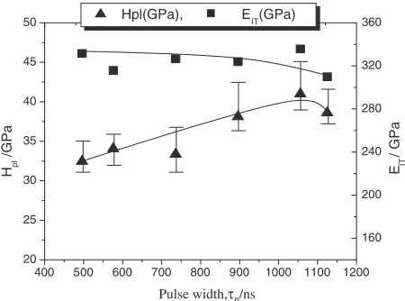
The dependence of the plastic hardness and Young’s modulus of the films on the pulse width is shown in Fig. 3. One can see that plastic hardness, Hpl, of the films ranges
between 32 to 41 GPa while the Young’s modulus, EIT, of
the films ranges from 320 to 340 GPa. The plastic hardness of the films increases on increasing the pulse width reaching to 41 GPa for 1056 ns of pulse width and decrease for higher pulse width, while the Young’s modulus of the films does not show any mentionable difference with changing pulse width.
The tribological properties of the films have been estimated from the variation ofH3=E2 ratio andWe(elastic
recovery) value of the films with pulse width which is shown in Fig. 4. TheH3=E2ratio reflects the resistance of a film to plastic deformation. It can be seen that bothH3=E2ratio and Wevalue of the films increased with increasing pulse width
and reach to its maximum at pulse width of 1056 ns and decrease for higher pulse width.
TEM observations were performed to determine the microstructure and phase formation of the films at low and high pulse widths. Figure 5(a) shows the plane view bright field TEM image of the film prepared under the low pulse width of 576 ns (D-2) corresponding to the polycrystalline structure. Analysis of related SAED pattern (Fig. 5(b)) reveals the existence of an fcc-CrN phase in the film.
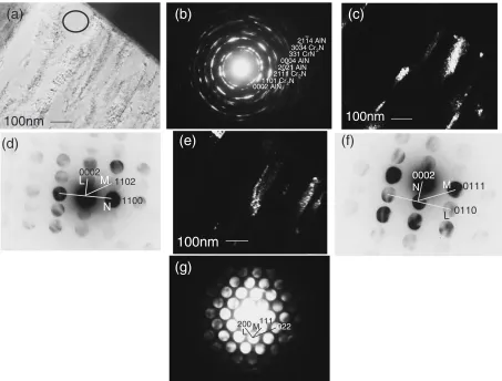
Figure 6(a) shows the cross sectional bright field TEM image of the film prepared under the high pulse width of 1056 ns (D-5) corresponding to the columnar structure. Analysis of related diffraction pattern of the film reveals the existence of a mixed structure of hcp-AlN, hcp-Cr2N and a small amount of fcc-CrN phases (Fig. 6(b)). Figure 6(c) is a dark field image for first ring of SAED pattern in Fig. 6(b) with hcp-AlN structure. The column width, obtained from the dark field image of the film, was in the range of 30–35 nm. In order to confirm the existence of hcp-AlN phase, micro-beam diffraction pattern was recorded from the hcp-AlN phase grains. The micro-beam diffraction pattern of the grain shown in Fig. 6(c) is seen in Fig. 6(d). Analysis of this diffraction pattern indicates the angles of 32 and 58 with N=L ratio of 1.55 and M=L ratio of 1.85, which is almost consistent with the hcp-AlN structure of a ½01110 oriented grain having the N=L and M=L ratios of 1.58 and 1.87 respectively. Figure 6(e) is a dark field image for second ring of SAED pattern in Fig. 6(b) with hcp-Cr2N structure. The column width, obtained from the dark field image of the film, was in the range of 25–33 nm. The micro-beam diffraction pattern of the grain shown in Fig. 6(e) is seen in Fig. 6(f). Analysis of this diffraction pattern indicates the angles of 29 and 61withN=Lratio of 1.08 andM=Lratio of 1.14, which is almost consistent with the hcp-Cr2N structure of a [1100] oriented grain having the N=L andM=L ratios of 1.09 and 1.13 respectively. Figure 6(g) shows microbeam diffraction pattern of the grain which is signed in Fig. 6(a). Analysis of this diffraction pattern indicates the angles of 35 and 54 with L=M ratio of 1.1 which is almost consistent with the fcc-CrN structure of a [011] oriented grain having theL=M ratios of 1.16.
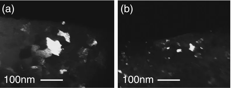
In order to compare the grain size of the films prepared at low (D-2) and high pulse widths (D-5), plane view dark field
400 600 800 1000 1200 0.0
0.5 1.0 1.5 2.0 2.5 3.0 3.5 4.0
Internal stress/GPa
Pulse width,τp/ns
Fig. 2 Influence of pulse width on internal stress values of CrAlN films.
400 500 600 700 800 900 1000 1100 1200
20 25 30 35 40 45 50
160 200 240 280 320 360
Hpl
/GPa
Hpl(GPa), EIT(GPa)
E
IT
/ GPa
Pulse width,τp/ns
Fig. 3 Influence of pulse width on hardness,Hpl, and Young’s modulus,
EIT, of CrAlN films.
500 600 700 800 900 1000 1100 1200 36
38 40 42 44 46 48 50 52
0.2 0.4 0.6 0.8 1.0
we
(%)
w e, H
3 /E2
H
3 /E
2
Pulse width,τp/ns
Fig. 4 Influence of pulse width onH3=E2ratio andW
[image:3.595.56.285.72.248.2] [image:3.595.313.538.74.239.2] [image:3.595.56.281.295.462.2]TEM images of each film are shown in Fig. 7(a) and (b) respectively. The grain size of the films at low pulse width of 576 ns (D-2) estimated from the dark field image of plane view TEM sample was in the range of 20–56 nm. On the contrary, the grain size of the film at the higher pulse width of 1056 ns (D-5), ranged from 2–20 nm. Clearly the grain sizes of films generated at higher pulse widths are comparatively smaller than that of films at lower pulse width. In this case,
it can be speculated that formation of two phases mutually inhibit each other’s grain growth and stimulates the renu-cleation of grains resulting in smaller grain size and enhanced hardness.17)
On the other hand, the grain sizes obtained from XRD peak width (Scherer’s formula), which indicate mean grain size measured perpendicular to the film surface, exhibited close values in the range of 9–18 nm for D-2 and D-5 films
(111) (200)
(220) (311)
(222)
(b)
100nm
(a)
Fig. 5 Plane-view TEM micrograph and corresponding electron diffraction patterns of the film with pulse width of 576 ns (D-2) (a) bright field image (b) SAED pattern with fcc-CrN structure.
100nm
100nm
100nm
(a)
(c)
(e)
0002 AlN1101 Cr2N 2111 Cr2N
2021 AlN0004 AlN 331 CrN3034 Cr2N
2114 AlN
(b)
N M L
1100 1102 0002
(d)
L
M N
0110 0111
0002
(f)
M
L 022
111 200
(g)
[image:4.595.84.513.73.222.2] [image:4.595.71.524.276.620.2](Table 1). These results indicate that D-5 film has grains which are 2–20 nm obtained from XRD analysis and 9–18 nm from TEM observation, and D-2 film consists of grains which are 18nm obtained from XRD analysis and 20–56 nm which obtained from TEM observation of the films.
4. Discussion
It is obvious from above results that pulse width influenced the microstructure and phase formation, which resulted in the different mechanical properties of the film. According to former research for CrNx deposition by reactive magnetron
sputtering, different phases such as Cr, CrþN, CrþNþ Cr2N, Cr2NþCrN, CrN can be obtained depending on nitrogen content.18–21) In this study, an fcc-CrN phase has
formed at lower pulse widths while a mixed structure of hcp-AlN, hcp-Cr2N and a small amount of fcc-CrN phases exists in the films at higher pulse widths. Lin et al.demonstrated that the maximum Nþ ion energy increased with a decrease of pulse width (increasing the duty cycle) at lower frequen-cies below 300 kHz in the Pulsed Closed Field Unbalanced Magnetron Sputtering system.8) Supposing that these
ten-dencies are kept even in the FTS system, lower pulse width resulted in the formation of fcc-CrN phase in the films. Although the sputtering process is a highly non-equilibrium process, the tendency of compound formation can be pre-dicted qualitatively using formation free energy (Ellingham diagram). Due to the smaller free energy of fcc-CrN phase in comparison with hcp-AlN and Cr2N phase as shown in Ellingham diagram, fcc-CrN phases is harder to form compared to AlN and Cr2N phases. Nþ ions having higher energy could facilitate the formation of CrN phase. On the other hand, as higher pulse widths decrease the maximum Nþ ion’s energy, CrN phase formation is probably suppressed, and consequently, the hcp-AlN and hcp-Cr2N phases preferentially form in the film. However, for the film with the highest pulse width (D-6), some metastable CrxNyphases
with broad range of composition have possibly formed in the film.22–24)
The intrinsic stress occurs as a consequence of an accumulation of crystallographic defects that are built in to the film during its deposition and is connected with the energy delivered to the growing film by bombarding ions
and condensing particles.25)Moiseevet al.showed that the
number of ions collected during the pulse-off time had a strong increase with the pulse-off time (= pulse width) in a Penning type magnetron sputtering system.26)Linet al.also
demonstrated that integrated Nþ ion flux in the plasma increased with increasing pulse width resulting in an incre-ment of internal stress of CrAlN film in the Unbalanced Magnetron Sputtering system.8,9) As can be seen from
Table 1, it might be supposed that there is a small difference in composition between D-2 and D-5 films. However, the D-5 film contains higher nitrogen than that of D-2. It should be noted that D-5 film consisting of Cr2N and AlN contains higher amount of nitrogen compared to D-2 film consisting of CrN phase. We conclude that excess nitrogen atoms were introduced to interatomic positions at higher pulse width, resulting in a higher internal stress of the film. Accordingly, an increase of Nþion flux at higher pulse widths leads to the increment of the internal stress with increasing pulse width as shown in Fig. 2.
Musil17) classifies the nanocomposite films with respect
to their microstructure as follows:
(Type-1) Nanocomposites with columnar microstructure composed of grains assembled in nanocolumns. There is an insufficient amount of the second (tissue) phase to cover the whole surface of all grains.
(Type-2) Nanocomposites with a dense microstructure composed of grains fully embedded in a tissue phase.
(Type-3) Nanocomposites with a dense globular micro-structure composed of a mixture of grains of different materials or of the same material with different crystallographic orientations and/or lat-tice structures.
It is important to note that D-5 film exhibiting the highest hardness contains a mixed structure of hcp-AlN, hcp-Cr2N and fcc-CrN phases, and consists of grains of 9–17 nm obtained from XRD analysis and 2–20 nm from TEM observations, which is finer compared to grains of17nm from XRD analysis and 20–56 nm from TEM observations for D-2 film. These facts characterize D-5 films as a nanocomposite film composed of a mixture of grains with different chemical composition (Type-3).
100nm
100nm
(a)
(b)
[image:5.595.101.499.73.225.2]Consequently, it is most likely that high internal stress, small grain size and formation of nanocomposite structure or a combination of all these is responsible for the higher hardness at higher pulse widths.
As can be seen in Fig. 3, the plastic hardness of the films increased with increasing the pulse width whereas the Young’s moduliis values of the films remain almost constant. Moreover, as described in Fig. 4, theH3=E2 ratio and the We value of the films increased with increasing
pulse width. These facts characterize the typical mechanical properties of nanocomposite films.27–29)From the view point of application in surface engineering, the feature of D-5 film with high resistance to plastic deformation and good tribological properties suggests usefulness of the film. Lin et al. reported that Cr-Al-N films exhibit good mechanical and tribological properties (Hpl41GPa, H3=E2 value 0:41) were obtained by P-CFUBMS of Cr and Al targets at a proper condition. They described that a higher hardness together with lower elastic modulus of thin films is ex-pected to allow the redistribution of the applied load over a large area, delaying failure of the film. Since the D-5 film exhibited the same hardness of 41 GPa, higher H3=E2 ratio of 0:6 and lower internal stress of3:5GPa in compar-ison with the Cr-Al-N films deposited by P-CFUBMS, this film may become a promising candidate for tribological applications. Thus, we conclude that a good combination of mechanical (hardness) and tribological properties of CrAlN films can be obtained by varying the pulse width even in a Balanced Magnetron Sputtering system.
5. Conclusion
From the results of the present study, the following conclusions can be drawn:
(1) Although there was an optimum pulse width at which the hardness of the CrAlN films reached their maximum values, the Young’s modulus value of the films remained almost constant.
(2) At lower pulse widths, films consisted of fcc-CrN structure while the structure changed to a mixed structure of hcp-AlN, hcp–Cr2N and a small amount of fcc-CrN phase at higher pulse widths.
(3) Increasing the pulse width resulted in an increase in the film’s internal stress. In addition, the grain size of the samples exhibited a tendency to decrease with increas-ing pulse width.
(4) Film with the highest hardness adopts typical properties of nanocomposite film composed of a mixture of grains of different materials.
(5) A good combination of mechanical (hardness) and tribological properties of CrAlN films can be obtained by varying the pulse width even in a Balanced Magne-tron Sputtering system.
Acknowledgement
The authors wish to express their thanks for the financial support by a grant for scientific research from Japan Society for the Promotion of Science. Grateful thanks are specially dedicated to Dr. Y. Sakamoto for help in executing the TEM sample preparation.
REFERENCES
1) G. Weigang, H. Hecht and G. von Minnigerode: Z. Phys. B96(1995) 349–355.
2) U. Wahlstrom, L. Hultman, J. E. Sundgren, F. Abidi, I. Petrov and J. E. Greene: Thin Solid Films235(1993) 62–70.
3) Y. Tanaka, T. M. Gur, M. Kelly, S. B. Hagstorm and T. Ikeda: Thin Solid Films228(1993) 238–241.
4) F. Vaz, L. Rebouta, M. Andritschky, F. M. da silva and J. C. Soares: Surf. Coat. Technol.98(1998) 912–917.
5) Y. Min, Y. Makino, N. Nose and K. Nogi: Thin Solid Films339(1999) 203–208.
6) J. Musil and H. Hruby: Thin Solid Films365(2000) 104–109. 7) H. Hasegawa, A. Kimura and T. Suzuki: Surf. Coat. Technol. 132
(2000) 76–79.
8) J. Lin, J. J. Moore, B. Mishra, W. D. Sproul and J. A. Rees: Surf. Coat. Technol.201(2007) 4640–4652.
9) J. Lin, J. J. Moore, B. Mishra, M. Pinkas, W. D. Sproul and J. A. Rees: Surf. Coat. Technol.202(2008) 1418–1436.
10) J. Lin, B. Mishra, J. J. Moore, W. D. Sproul and J. A. Rees: Surf. Coat. Technol.201(2007) 6960–6969.
11) H. Willmann: Scr. Mater.54(2006) 1847–1851. 12) R. Wuhrer: Scr. Mater.50(2004) 1461–1466.
13) H. Hasegawa: Surf. Coat. Technol.188–189(2004) 234–240. 14) M. Fenker, M. Balzer and H. Kappl: Thin Solid Films 515(2006)
27–32.
15) A. Mumtaz and W. H. Class: J. Vac. Sci. Technol.20(1982) 345. 16) M. Nose, W. A. Chiou, M. Zhou, T. Mae and M. Meshii: J. Vac. Sci.
Technol. A20(2002) 823–828.
17) A. Cavaleiro, Jeff, Th. M. De Hosson: ‘‘Nanostructured Coatings’’ Springer, (2006) p. 412.
18) C. Rebholtz, H. Ziegele, A. Leyland and A. Matthews: Surf. Coat. Technol.115(1999) 222–229.
19) G. Wei, A. Rar and J. A. Barnard: Thin Solid Films398–399(2001) 460–464.
20) P. Hones, N. Martin, M. Regula and F. L’evy: J. Phys. D: Appl. Phys.
36(2003) 1023.
21) G. A. Zhang, P. X. Yan, P. Wang, Y. M. Chen and J. Y. Zhang: Mater. Sci. Eng. A460–461(2007) 301–305.
22) J. P. Terrat, A. Gaucher, H. H. Rabah and R. Y. Fillit: Surf. Coat. Tech.
45(1991) 59–65.
23) M. Charbonier, M. Romand, A. Roche and J. P. Terrat: Adv. X-ray Anal.35(1992) 819.
24) Y. G. Chang, R. K. Warsop, N. E. Farb and R. Parsons: Surf. Coat. Technol.68–69(1994) 157–165.
25) J. Musil, V. Poulek, V. Valvoda, R. Kuzel, Jr., H. A. Jehn and M. E. Baumgatner: Surf. Coat. Techol.60(1993) 484–488.
26) T. Moiseev and D. C. Cameron: Surf. Coat. Technol.200(2006) 5306– 5317.
27) J. Musil and H. Polacova: Surf. Coat. Technol.127(2000) 99–106. 28) J. Musil, P. Zeman, H. Hruby and P. H. Mayrhofer: Surf. Coat.
Technol.120–121(1999) 179–183.