Developing Power Semiconductor Device Model for
Virtual Prototyping of Power Electronics Systems
Ke Li, Paul Evans, Mark Johnson
Power Electronics, Machine and Control groupUniversity of Nottingham, UK
Email: [email protected], [email protected], [email protected]
Abstract—Virtual prototyping (VP) is very important for power electronics systems design. A virtual prototyping design tool based on different modelling technology and model order reduction is proposed in the paper. In order to combine circuit electromagnetic model with power semiconductor device models, a SiC-JFET behavioural model is presented and implemented in the design tool. A half bridge circuit using SiC-JFET devices is thus represented in the VP software. The presented SiC-JFET behavioural model is then validated by comparing with experimental measurements on switching waveforms.
Keywords—Virtual prototyping; Model order reduction; Power semiconductor device modelling; Behavioural model; Switching waveforms
I. INTRODUCTION
Power electronics systems are essential in the drivetrain of hybrid and electrical vehicles. Optimising the design of these systems is important in increasing performance, such as reducing overall drivetrain weight and size, improving efficiency so as to increase range, and ensuring a robust and reliable drivetrain [1].
Optimising system design through the construction and testing of physical prototypes can be time-consuming and expensive. Thus, virtual prototyping (VP) techniques offer one solution to eliminate the requirement for construction and testing of physical prototypes, which could reduce design time and costs so as to realize highly optimised system designs. A key requirement for VP is the ability to predict the performance of a design by using only simulation, which could help designers to obtain reliable results in a quick way. Thermal design and electromagnetic compatibility design are very important for power electronics systems used in electrical vehicles, in which automotive drivetrain could reach more than 100kW power rating. At one side, even at system efficiencies greater than 95%, the large quantities of waste heat produced require an efficient thermal design. Thus, it is necessary that power devices (passive and active) losses and heat path from each heat source to the cooling equipment could be accurately and fast simulated in order to evaluate system thermal performance. At another side, the switching nature of the power semiconductor devices introduce high dI/dt and dV/dt which necessitates careful consideration in terms of electromagnetic performance. Thus, it is necessary that both electromagnetic interference (EMI) source and its propagation loop could be well represented, so power semi-conductor devicedI/dt,dV/dt transition and parasitic elements
shall be accurately and efficiently simulated. Moreover, the fast time-constants (nanoseconds) associated with the power semiconductor devices, slow time-constants (minutes) associ-ated with thermal effects, and requirement for 3D modelling of the system design, mean that novel, efficient simulation techniques and design tools are required to avoid excessively long simulation times.
Developing a VP design tool which can predict the above performance could help designers to previously validate their prototype prior to experimental measurements. A VP design tool has been proposed by authors in [2], [3], where power electronics system thermal performance has been validated. However, accurate modelling of the power semiconductor device was found to be a limitation in the above papers. Thus, in this work, it will be presented that how efficient behavioural semiconductor models can be when they are combined with model order reduction techniques for 3D system simulation to allow rapid virtual prototyping of power electronic systems.
The paper is structured with following parts. At first, modelling techniques of the proposed VP design tool for power electronics systems will be reviewed. Then, power semiconductor device behavioural model will be presented. Afterwards, a half bridge circuit using SiC-JFET is represented by the VP design tool. Simulation results and experimental measurements of device switching current and voltage are compared, which is followed by the conclusion.
II. MODELLING TECHNIQUES OFVIRTUAL PROTOTYPING DESIGN TOOL
A. Efficient Device Modelling
Components whose physical location will influence system performance such as bus-bars, PCBs and heatsinks, can-not use simplistic behavioural models. The 3D geometry of these components influences system performance and will be changed during the system optimisation process by designers, so a simulation model capable of capturing the effect of these changes must be used. Accelerating these physical, 3D simulations is essential to allow fast simulation times, which will be presented in the next part.
B. Efficient Modelling of the 3D Design Geometry
To fully evaluate the performance of a design, numeri-cal methods must be used to translate design details such as geometry and construction materials into an equivalent mathematical model. One most used technique is spatial discretisation (meshing) which generates a large system of Ordinary Differential Equations (ODE) by dividing the design geometry into many small sections or elements over which a solution describing the effects of interest can be written. Thus, thousands of elements, resulting in a system of thousands of ODEs, can be necessary to obtain accurate results. In the software developed, the approach based on Finite-Difference Method (FDM) is used for thermal simulation and that based on Partial Element Equivalent Circuit method (PEEC) is used for electromagnetic simulation.
In order to increase simulation speed, Model Order Reduc-tion (MOR) techniques to reduce the number of equaReduc-tions generated by the discretisation is applied in the VP design tool. The principle of MOR techniques is that if a discretisation produces n ODEs, which give rise to n eigenvalues spread over the model frequency response range, the solution can in fact be accurately represented using a much smaller number of m eigenvalues. Krylov subspace project algorithms are used to find a much smaller system of mODEs which accurately capture the original dominant eigenvalues, where m n. As expressed in eq. (1), the algorithm produces an m×nmatrix H and its transposeHT with orthonormal rows which can be
used to link original state vectorsxto its reduced order vector xr.
xr= [H]x
x= [H]Tx r
(1)
Thus, a reduced order system with following new equations linking the input u of size a and output y of size b of the original system could be obtained by applying eq. (1).
[H]M[H]Tx˙
r= [H]A[H]Txr+ [H]Bu
y=C[H]Txr
(2)
[Mr] ˙xr= [Ar]xr+ [Br]u
y= [Cr]xr
(3)
The reduced ordered matricesMr,Ar,BrandCrarem×m,
m×m,m×aandb×mmatrices, of which the size is much
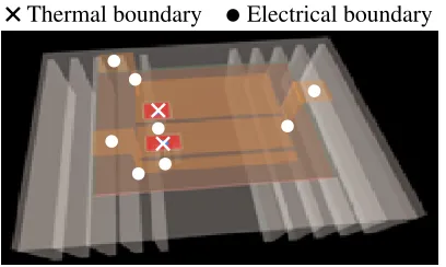
Electrical boundary
Thermal boundary
Fig. 1: Defined boundaries in geometrical model
G
D
S
D
S G
Cgd
Cgs Cds
Gch
[image:2.612.335.539.48.170.2]Rbd Rbds
Fig. 2: Equivalent circuit of a transistor
smaller than their original onesM (n×n),A(n×n),B(n×a) and C (b×n). Thus, only m equations need to be solved at each time-step. No spatial information is lost, as variables such as the voltage, current, temperature and heat-flux values at any node in the original model can be calculated from the reduced order states using theHT matrix (eq. (1)). Therefore
full 3D graphical analysis, at any time-step, is still possible. The volume of data required to be stored and processed for long simulations is also significantly reduced.
The software applies an Arnoldi MOR algorithm [5] for thermal order reduction, and the related PRIMA [6] algorithm for electromagnetic order reduction. The accuracy of these techniques when applied to a typical power electronic sim-ulation is shown in [3].
C. Coupled Physical and Behavioural Model Description
The 3D design geometry is defined in terms of building blocks such as 3D solids, along with a set of electrical and thermal boundaries. These basic building blocks can be grouped to form components such as power modules, substrate tiles, heat-sinks or bus-bars. The boundaries serve as points to which the behavioural models of the remainder of the system can be connected for design evaluation, which is shown in Fig. 1. Electrical boundary can be used to connect with other electrical part for electrical simulation while thermal boundary can be used to connect with other thermal part for thermal simulation.
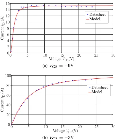
[image:2.612.334.539.203.301.2]semiconduc-VoltageVDS(V)
0 5 10 15 20 25 30
Current
ID
(A)
0 2 4 6 8 10 12 14 16
Datasheet Model
(a)VGS=−9V
0 5 10 15 20 25 30
0 20 40 60 80 100
VoltageVDS(V)
Current
ID
(A) DatasheetModel
[image:3.612.73.274.47.290.2](b)VGS=−3V
Fig. 3: SiC-JFET static characteristics comparison of different VGS voltages
tor device behavioural model will be presented in the next section.
III. POWER SEMICONDUCTOR DEVICES MODELLING A unipolar power transistor can be generally modelled with the equivalent circuit shown in Fig. 2, which is presented by authors in [7]–[9] to model SiC-JFET, SiC-MOSFET and GaN-HEMT. Current source Gch represent power transistor
forward static characteristics, which is controlled by both VDS and VGS voltages. Body diode static characteristic is
represented by a non-linear resistor Rbd and a constant
resistor Rbds. The dynamic behaviour is modelled by three
non-linear capacitors Cgd, Cds and Cgs and each capacitor
is only dependent on the voltage across it. Depending on device structure and packaging type, internal gate resistor and parasitic inductances could be added in this model.
A. Static characteristics modelling
A “Normally-on” SiC-JFET (IJW120R070T1, 1200V/35A, Vth≈ −13.5V) is modelled in this subsection.
When VGS > Vth, at one VGS voltage, the following
equation can be used to represent the VDS-ID curve. All the
parameters a, b and c in the above equation could be obtained based on datasheet or the measured values through fitting method by usingf minconfunction in MATLAB.
ID=a−
a
1 + VDS b
c (4)
The comparison between the model and the datasheet is shown in Fig. 3 at differentVGSvoltages. It is shown that the
chosen simple function can represent well the device static
-12 -10 -8 -6 -4 -2 0 2 4
V
alue
10−2
VoltageVGS(V) 10−1
100 101 102 103
[image:3.612.336.537.50.161.2]a bc a(Func.) b(Func.) c(Func.)
Fig. 4: Comparison between the function and the obtained parameters in eq.(4)
characteristics. The value of the parameters in eq.(4) can then be obtained on different VGS voltage values. Following
equation eq.(5) could represent the evolution of each parameter (when VGS> Vth), wheres indicates parameter a, b, c. The
values of s1-s4 are given in TABLE. I.
s= s1 1 +VGS−Vth
s2
s3 +s4 (5)
TABLE I: s1-s4 values in eq.(5) for each parameter (various
units without physical meaning)
s s1 s2 s3 s4
a -1.05×10⁴ 71.46 2.4 1.05×10⁴
b -1.3×10⁴ 321.3 2.27 1.3×10⁴
c 6.13 1.98 0.8 0
The comparison between eq.(5) and the obtained parameters in eq.(4) is shown in Fig. 4. The value of each parameter out of the datasheet range is obtained by extrapolation of the eq.(5). When device is reverse conducted, conduction current ISD could be represented by the sum of the device channel
current Ich and body diode current Ibd, where non-linear
resistorRbdcould be represented by the following equation, in
whichVbdis the voltage acrossRbd. Parametersabd= 2.66Ω,
bbd = 1.38V, cbd = 1.244 andRbds = 0.001Ω are used to
model body diode static characteristic. Thus, the comparison between the datasheet and the model is shown in Fig. 5, where it is shown that the model represents well the device static characteristics. However, the difference between the model and the datasheet relies mainly on the difference between the chosen function and the parameters in Fig. 4.
Rbd=
abd
1 +Vbd bbd
cbd (6)
B. Dynamic characteristics modelling
The nonlinearity of both Cgd and Cds are expressed by
following mathematical function whenVx is inferior to 500V:
Cx=
a
1 + Vx b
0 5 10 15 20 25 30 35 40 45 50 0
50 100 150 200 250
VoltageVDS(V)
Current
ID
(A) VGS= 2V
VGS= 0V
VGS=−3V
VGS=−6V
VGS=−9V Model
Datasheet
(a) Forward conduction
0 1 2 3 4 5 6 7
0 5 10 15 20
VoltageVSD(V)
Current
ISD
(A)
Model Datasheet
VGS= 0V
VGS=−20V
VGS=−5V
[image:4.612.74.275.46.315.2](b) Reverse conduction
Fig. 5: Comparison between the model and the datasheet on SiC-JFET static characteristics
whereCxis the capacitance value andVxis the voltage across
the capacitor. In the range where Vx is superior to 500V, Cx
is expressed by a constant capacitance value.
VoltageVDS(V)
0 100 200 300 400 500 600 700 800
Capacitance
C
(pF)
103
102
101
Cgd Cds
Datasheet
ModelCds Datasheet
ModelCgd
[image:4.612.309.565.58.311.2](a)Cds values
Fig. 6: Comparison on inter-electrode capacitance values and their models
The comparison between inter-electrode capacitances datasheet values and their values are shown in Fig. 6, which shows that both Cgd and Cds are expressed well by the
chosen functions. For Cgd capacitance, the used parameters
are a= 2.5×10⁴(pF), b= 3.58
×10−4(V), c= 0.464, d=
2 ×10⁴(pF), e = 0.22(V−1) and for C
ds capacitance, the
used parameters are a= 647(pF), b= 3(V), c = 0.398, d= 210.4(pF), e= 0.038(V−1).
Lpara
V
Rg
Rg
S1 S2
Lpara
Cbus
Load Switching mesh
(a) JFET half bridge electrical circuit
Load connector
Current measurement loop Cbus
S2
S1
Driver circuit
Driver circuit
(b) JFET half bridge switch-ing circuit
Cbus S2
S1 load connector driver
connectors driverconnectors
V+ V−
(c) JFET half bridge switching circuit representation Fig. 7: JFET half bridge circuit and its representation
Cgs is assumed to be a constant capacitor and its value is
the same as given in datasheet: 1.6nF.
The presented SiC-JFET model will then be implemented in the presented VP design tool. Device switching waveforms of the simulation will be compared with experimental mea-surements.
IV. EXPERIMENTAL VALIDATION
A. SiC-JFET half bridge circuit representation
The SiC-JFET half bridge electrical circuit is shown in Fig. 7a, which is mainly constructed by a bus capacitorCbus,
two SiC-JFETs S1 and S2, driver circuit of each device and an air-core inductor as the load.
The switching mesh of the circuit is shown in Fig. 7b, where parasitic inductances could be found not only in the switching current loop, but also in the driver circuit.
The switching circuit is then represented in the VP design tool, in which the PCB track of the switching mesh is rep-resented with their geometric information. The power supply, Cbus, SiC-JFETs S1 and S2, device driver circuits and load
are represented by their corresponding behavioural models in the simulation circuit through electrical boundaries, which are shown as blue points in Fig. 7c, where switching loop parasitic inductance Lpara values are determined by the 3D meshed
model.
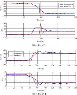
SiC-JFET S1 switching current ID and switching voltage
VDSare compared between the measurement and simulation,
[image:4.612.50.299.423.575.2]B. Comparison results
Current ID and voltage VDS are compared in the three
conditions below. In condition 1, simple SiC-JFET device model (ideal switch with a parallel RC branch) as that presented in [3] is used and parasitic inductance values are extracted by the software. In condition 2, the presented SiC-JFET model is used, however there is no parasitic inductance values extracted. In condition 3, the presented SiC-JFET model is used while parasitic inductance values are extracted and used in the simulation.
1) Condition 1: The comparison between the measurement and the simulation in this condition is shown in Fig. 8. The simple device model could not represent good ID and VDS
switching transitions, because the capacitance value in the model is constant and there is no capacitive coupling (Miller effect) between drain and gate of the device. The obtained switching energies of the simulation are: Eon = 0.5µJ and
Eoff = 11µJ, which is far from those of the measurement:
Eon= 165µJandEoff = 25µJ. Thus, the ideal model yields
an inaccurate switching loss as the measurement.
Time(ns)
Vds(V)
-1000 100 200 300 400 500
Time(ns)
Id(A)
-10 0 10 20 30 40
0 50 100 150 200
0 50 100 150 200
Simulation Measurement
(a) JFET ON
Time(ns)
Vds(V)
-200 0 200 400 600
Time(ns)
Id(A)
-5 0 5 10 15
Simulation Measurement
0 20 40 60 80 100 120 140 160 180
0 20 40 60 80 100 120 140 160 180
[image:5.612.311.565.106.412.2](b) JFET OFF
Fig. 8: JFET switching waveforms comparison of condition 1
2) Condition 2: The comparison between the measurement and the simulation in this condition is shown in Fig. 9. As parasitic inductances in the circuit are not extracted, LC resonance at the end of the turn-ON and turn-OFF switching are not represented in the simulation. Meanwhile, device turn-ON dI/dt transition is much faster than measurement,
which yields a bigger turn-ONID peak current. The obtained
switching energies of the simulation are: Eon = 218µJ and
Eoff = 34µJ, which is close than ideal model but still different
from the measurement.
Time(ns) -200
0 200 400 600
0 20 40 60
0 50 100 150 200
Vds(V)
Time(ns)
Id(A)
0 50 100 150 200
Simulation Measurement
(a) JFET ON
Time(ns)
Vds(V)
0 200 400 600
Time(ns)
Id(A)
-5 0 5 10 15
0 20 40 60 80 100 120 140 160 180
0 20 40 60 80 100 120 140 160 180
Simulation Measurement
[image:5.612.49.299.304.614.2](b) JFET OFF
Fig. 9: JFET switching waveforms comparison of condition 2
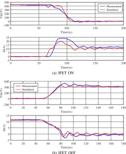
3) Condition 3: The comparison between the measurement and the simulation in this condition is shown in Fig. 10, where it shows that device switching waveforms are closer to the measurement by adding parasitic inductances and the presented device behavioural model. The simulation represents generally well the measurement on both current, voltage transition andLC resonance at the end of the switching. LC resonance frequency is accurately represented, which demon-strates that device output capacitance valueCossand switching
loop parasitic inductances are well simulated. Device turn-OFF dI/dt and dV/dt are represented well by the simulation. The main difference between the measurement and the simulation is the turn-ON switching transition, which is mainly due to the inaccurate representation of the stored charge in the simulation when upper device S2 is reverse conducted. Future work will be focused on how to correctly represent this parameter in the model. The obtained switching energies of the simulation are: Eon= 148µJand Eoff = 28µJ, which are closer to the
measurement than above two conditions.
equation model to 23 equation model in order to accelerate simulation speed. The presented device model could be also used in circuit simulation software such as PSPICE. However, as parasitic inductances could influence on device switching waveforms, their values including mutual inductances of the switching mesh are necessary to be extracted and added in simulation circuit, which might consume lots of time.
Time(ns)
0 50 100 150 200
Vds(V)
-1000 100 200 300 400 500
Time(ns)
Id(A)
-50 5 10 15 20 25
0 50 100 150 200
Simulation Measurement
(a) JFET ON
Time(ns)
0 20 40 60 80 100 120 140 160 180
Vds(V)
-200 0 200 400 600
Time(ns)
Id(A)
-5 0 5 10 15
Simulation Measurement
0 20 40 60 80 100 120 140 160 180
[image:6.612.49.300.147.455.2](b) JFET OFF
Fig. 10: JFET switching waveforms comparison of condition 3
V. CONCLUSION
A virtual prototyping (VP) design tool using power semi-conductor device behavioural models is presented in the paper. Different modelling techniques are used to model different components in the design tool and by using model order reduction algorithms, simulation speed could be increased.
A behavioural model of a SiC-JFET is then presented, in which device static and dynamic characteristics are represented by mathematical functions. The model is then implemented in the VP design tool, where a SiC-JFET based half bridge circuit is represented. By comparing with the simulation of a simple device model and the simulation without parasitic inductances extraction, it is shown that circuit electromagnetic model together with power semiconductor device behavioural model could represent well device switching waveforms, so device switching losses can be accurately calculated. Future work will include thermal model based on the presented results, so as to evaluate device electrical thermal performance.
ACKNOWLEDGMENT
The authors would like to thank UK Engineering and Phys-ical Sciences Research Council (EPSRC) power electronics center for the financial support and all the partners of the project Multidomain Optimization and Virtual Prototyping for High-Density Power Electronics Systems for technical discussions.
REFERENCES
[1] A. Emadi, S. S. Williamson, and A. Khaligh, “Power electronics intensive solutions for advanced electric, hybrid electric, and fuel cell vehicular power systems,” IEEE Transactions on Power Electronics, vol. 21, pp. 567–577, May 2006.
[2] P. Evans, A. Castellazzi, and C. Johnson, “A multi-disciplinary virtual prototyping design tool for power electronics,” in Integrated Power Systems (CIPS), 2014 8th International Conference on, pp. 1–7, Feb 2014. [3] P. Evans, A. Castellazzi, and C. Johnson, “Design tools for rapid multido-main virtual prototyping of power electronic systems,”Power Electronics, IEEE Transactions on, vol. 31, pp. 2443–2455, March 2016.
[4] H. Wu, R. Dougal, and C. Jin, “Modeling power diode by combining the behavioral and the physical model,” in31st Annual Conference of IEEE Industrial Electronics Society, 2005. IECON 2005., pp. 6 pp.–, Nov 2005. [5] T. Bechtold, E. B. Rudnyi, and J. G. Korvink,Fast Simulation of
Electro-Thermal MEMs. Freiburg: Springer, 2006.
[6] A. Odabasioglu, M. Celik, and L. T. Pileggi, “Prima: passive reduced-order interconnect macromodeling algorithm,” in Computer-Aided De-sign, 1997. Digest of Technical Papers., 1997 IEEE/ACM International Conference on, pp. 58–65, Nov 1997.
[7] T. Funaki, A. Kashyap, H. Mantooth, J. Balda, F. Barlow, T. Kimoto, and T. Hikihara, “Characterization of SiC JFET for Temperature Dependent Device Modeling,” in Power Electronics Specialists Conference, 2006. PESC ’06. 37th IEEE, pp. 1 –6, june 2006.