1
Optimization for approximate softcore
unsigned multipliers on Altera FPGA’s
2
Abstract
In applications where a certain degree of error is allowed in applied operations or where a certain degree of error is already present in the input data, so-called ‘approximate computing’ can be replace traditional computations and can provide synthesis area or power consumption savings by using alternative operations which may contain an error in the output. This work proposes new approximate unsigned multiplication schemes in Altera FPGA architectures and compares these to existing designs using the metrics accuracy, synthesis area and power consumption.
The existing 2-bit by 2-bit approximate multiplier proposed by Kulkarni et al. [1] is implemented in the Altera Cyclone IV and Cyclone V FPGA architectures and used to create an 8-bit by 8-bit multiplier, making use of the scheme to combine multipliers introduced in the same paper. This existing 2-bit by 2-bit design is modified for a new 4-bit by 2-bit approximate multiplier design, optimised for Cyclone V (and Stratix V and newer) architecture, which in theory should provide synthesis size and power consumption savings. For optimising the addition of partial products, simple shifting and adding is compared to Wallace tree compression and a new rearrangement scheme for more efficient addition of the partial products. The multiplication schemes were compared for uniform distributions and normal distributions with varying densities.
The implementation of 2-bit by 2-bit approximate multiplication was not able to outperform the default multiply operator in Cyclone IV in power consumption or synthesis area, even
disregarding the error it introduces. Although the 4-bit by 2-bit multiplier performed better than the default multiply operator in Cyclone IV, this only shows that the default multiply operator is poorly optimized and allows room for more efficient multiplication, since the 4-bit by 2-bit design was not designed to be efficient in Cyclone IV architecture. Measuring power consumption in Cyclone V is not possible, but synthesis size results show that the 4-bit by 2-bit design was not implemented in the intended optimised manner.
3
Contents
Abstract... 2
Introduction ... 4
Background ... 5
Binary multiplication ... 5
Adder structures... 6
Approximation ... 6
Approximate multiplication ... 6
Field Programmable Gate Array architecture ... 7
Research methodology ... 8
Research questions ... 8
Proposed design factors to be researched ... 8
2-bit by 2-bit approximate and accurate multiplication on FPGA ... 8
Architecture optimized 4-bit by 2-bit partial multiplication ... 8
Approximate 4-bit by 2-bit multiplication ... 9
Adder optimization: rearranging ...10
Adder optimization: compression ...10
Mathematical analysis ...11
Behavioural model ...14
Testing setup ...17
Results ...19
Approximate multiplier designs ...19
Adder designs ...21
Discussion and recommendations...24
Recommendations...24
Conclusion ...25
Appendix: Approximate multiplier designs ...26
References ...30
4
1. Introduction
Multiplications and multiply-accumulate operations are often used in computations and
especially with any physics-based calculations. When processing real-world data, there is often a certain measure of acceptable error during processing, due to noise causing measurement errors in the input data or because any imperfections in the output will go unnoticed, for example in video decoding.
Approximate computing makes use of this leeway, by trading accuracy for using fewer computational resources or less power consumption. This means that the output of a certain multiplication or addition might have a chance of containing a certain error, but that the operation can be completed with a simpler logic circuit or while consuming less energy. In this work the following question is examined:
- What is the best scheme for approximate multiplication in FPGA in the trade-off between accuracy and power?
This was then subdivided in the following questions
- What partial multiplication scheme in FPGA gives the best results in the trade-off between accuracy and power?
- What addition scheme in FPGA for the addition of the partial results gives the best results in the trade-off between accuracy and power?
In 2011, Parag Kulkarni et al. introduced an approximate multiplier where the logic for the multiplier was reduced resulting in an erroneous output for one of the 16 input combinations and additionally introduced a method to combine multiple small multipliers in arbitrarily large
multipliers [1]. This work takes these concepts as its basis but implements them in FPGA architecture to see if approximate multiplication with this method is viable on FPGA architecture and to see what multiplication scheme would be best for it.
Based on Kulkarni’s approximate multiplier design, a new design is introduced in this work which is optimized for the new Altera Cyclone V FPGA architecture. Additionally, as Kulkarni’s method of making arbitrarily large multipliers makes use of several smaller multipliers which produce partial products that must be added together, two addition schemes are examined: Wallace tree compression and a proposed new method based on rearranging the partial products based on their bit shifting.
5
2. Background
Binary multiplication
In real world computing many operations require multiplication. In general, multiplication in binary takes on a two-step approach: generating partial products and adding these partial results together to form the final product of the multiplication. A basic method for executing this operation in binary is ‘shifting and adding’, where every partial result is calculated by the multiplication of 1 bit of the multiplier by x bits of the multiplicand, where x is the length of the multiplicand. In a 4-bit by 4-bit multiplication, this would produce 4 partial products of 4-bits. The result is obtained after adding together all generated partial products. This process can be seen in Figure 1: Shift and add multiplication
Figure 1: Shift and add multiplication
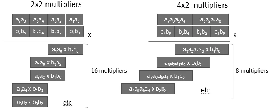
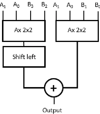
Another approach for binary multiplication is using smaller partial multipliers. Utilising the combinational logic displayed in Fig. 2,a 2-bit by 2-bit partial multiplier can be generated which computes the result of a 2-bit by 2-bit multiplication. This multiplier can then be used as a building block to build larger multipliers as displayed in Fig. 3. In this multiplier design four [2] 4-bit partial results are generated, which will have to be added to produce the result of the
multiplication.
[image:5.612.77.489.488.656.2]6
Adder structures
In the discussed multiplication schemes, the generated partial products must be added to produce the result of the multiplication. Furthermore, the accumulation step in a multiply-and-accumulate unit is also an additional add operation. The adding of partial products is
traditionally done in a shift-add structure, where all partial products are left-shifted the relevant amount of positions and then added together.
A more efficient method for adding together more than two numbers, on which modern adding structures are still based, was presented in the 1960’s, called the Wallace Tree [2]. This structure uses full adders and half adders to process the addition of all partial products in a more resource- and time efficient manner than shift-adding. Full adders can be seen as 3:2-bit compressors: they process 3 input bits to 2 output bits, reducing the total amount of bits that will have to be added. These can all work in parallel, without having to wait for a carry line. The Wallace Tree compresses all partial products until there are only 2-bits left for each bit position, requiring 1 final addition operation, which can then be carried out with a carry-adder.
Approximation
In many applications it is not necessary for the results of computations to be perfectly accurate. In image and video processing this might for example be because any imperfections in the result are not noticeable for the human observer. It is also possible for the operation inputs to already contain a certain degree of error. Errors introduced by an inaccurate operation may be less critical as the reliability of the output is already lowered due to the chance of errors in the input. If perfect accuracy is not required, alternative operations can be executed to approximate the result of the original operation, while possibly utilising fewer resources.
Approximate multiplication
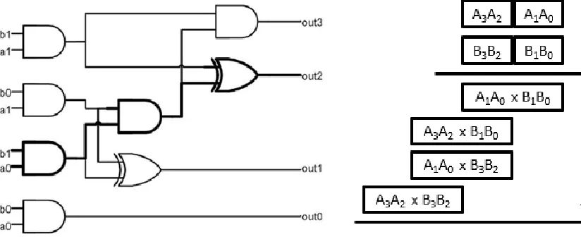
[image:6.612.87.528.515.677.2]In the paper ‘Trading Accuracy for Power with an Underdesigned Multiplier Architecture’ [1], an alternative design is introduced for the 2-bit by 2-bit partial multiplier. A reduction in logic leads to a reduction in the amount of output bits, lowering it from 4 to 3, forgoing the most significant bit. Because of this, one of the 16 possible outcomes cannot be computed correctly. This result is approximated by producing the output “111” in binary, resulting in an error of magnitude 2 or 22.2%. The logic circuit for this design can be seen in Figure 4: The accurate multiplier on the left and the approximate version on the right [1].
7
Field Programmable Gate Array architecture
A Field Programmable Gate Array (FPGA) is a system which can provide combinational logic functionality through programmable logic blocks and programmable interconnects. This contrasts with combinational logic functionality on ASIC where the components of the combinational logic are created with silicon structures. The programmable logic blocks of FPGA’s often contain a Lookup Table (LUT) to emulate combinational logic, as well as memory elements like registers and arithmetic specific components like adders. The programmable LUT can match a certain output with any combination of inputs, emulating the behaviour of a
[image:7.612.130.492.260.432.2]combinational logic circuit. In Figure 5 the architecture of a logic block or Adaptive Logic Module (ALM) in the Altera Cyclone V architecture can be seen. Cyclone IV architecture uses Logic Elements (LE) as their logic blocks (not depicted). For clarity, the Cyclone V architecture from now on will be referred to as the ALM architecture, while the Cyclone IV architecture will be referred to as the LE architecture.
8
3. Research methodology
Research questions
The initial goal of the assignment was to study the trade-off between cost (power and synthesis area) vs quality (accuracy of computed results) of approximate computation in FPGA designs. This was to be done for a multiply-accumulate (MAC) module implemented in FPGA that could handle 8-bit fixed point, unsigned input streams with various distributions.
Initially, multiplication combined with efficient adder integration for a Multiply-and-Accumulate unit were researched, as done by Kumm et al [3], with the additional step of using approximate multiplication. The synthesis control needed for the optimization in the addition was not within reach for this assignment, after which focus shifted to the implementation of the approximate multiplication. The schemes that were used for this, still required the addition of partial results, but the accumulation part of the module was removed so that power consumption results of the multipliers were able to be compared more effectively.
The research question on which this research then focused are the following:
- What is the best scheme for unsigned approximate multiplication in FPGA in the trade-off between accuracy, area and power consumption?
This was then subdivided in the following questions
- What partial multiplication scheme in FPGA gives the best results in the trade-off between accuracy and power?
- What addition scheme in FPGA for the addition of the partial results gives the best results in the trade-off between accuracy and power?
Proposed design factors to be researched
2-bit by 2-bit approximate and accurate multiplication in FPGA
The 2-bit by 2-bit approximate multiplier design by Kulkarni [1] (referred to as Ax2x2) was the first design chosen to test the viability of approximate multiplication in FPGA. When the design is implemented in FPGA, the reduction in logic does not translate directly to the reduction in resources in FPGA architecture, where combinational functions are emulated with Look-Up-Tables (LUT).
When Kulkarni’s multiplier design is implemented in FPGA, each LUT processes all 4 input bits and produces a single output bit. This means that an accurate 2-bit by 2-bit multiplier (Acc2x2) using this method would require 4 LUT’s to produce 4 output bits. By reducing the required output bits from 4 to 3 in the approximate version, the amount of required LUTs is also reduced from 4 to 3, a 25% saving.
Both the approximate and accurate 2-bit by 2-bit multipliers are examined in this work.
Architecture optimized 4-bit by 2-bit partial multiplication
Over time, FPGA architecture changes to accommodate more complex designs. By studying the underlying concepts of modern architectures, it is possible to optimise designs for these new architectures.
9 functions and produce a 1-bit output. The ALM architecture makes use of 8-input LUT’s, which can provide the same functionality as two 4-input LUTS, but additionally can be used to process a single larger function with up to 7 inputs [4]. With certain restrictions (“If two 6-input functions
[image:9.612.82.531.152.337.2]have the same logic operation and 4 shared inputs”) an ALM is even able to process up to two 6-input functions. [4]
Figure 6: Comparison between theoretical resource usages of different sized partial multipliers
Keeping these restrictions in mind, a new design for a partial multiplier is introduced that could provide better performance in the new architecture. This partial multiplier takes one 4-bit input and one 2-bit input and produces the 6-bit output. Figure 6 gives an overview of the theoretical resource usage for an 8-bit by 8-bit (8x8) multiplier built out of 4-input LUT’s and 2x2 partial multipliers versus the resources used by a multiplier designed with the 6-input LUT’s and 4x2 partial multipliers.
A single ALM can process two 4-input or two 6-input functions. An Acc2x2 multiplier requires four 4-input function and an Acc4x2 multiplier requires 6 input functions. As shown in Fig. 6, a 6-input partial multiplier can process an 8-bit by 8-bit multiplication more efficiently in the ALM architecture than a 4-input partial multiplier.
Furthermore, when the following addition of the partial products is taken into account, one can see that more gains are begotten as the 4x2 multipliers result in a smaller total size of partial products that must be added.
Approximate 4-bit by 2-bit multiplication
Building further on this concept, an approximate version of the 4x2 multiplier was made based on the same principles as the 2x2 approximate multiplier designed by Kulkarni et al. This
10
The resource usage reduction with this approximate multiplier is also 1 combinational function (equal to 1 LE or ½ ALM), which relatively is a smaller saving in resources compared to the accurate design than the Ax2x2 multiplier achieved. When this is combined with the inherent area savings which the accurate 4x2 design introduces, as shown in the previous paragraph, the design is found to be competitive with the Ax2x2 design and could provide an improved alternative for approximate multiplication in the ALM FPGA architecture.
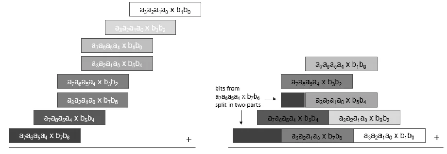
Adder optimization: rearranging
[image:10.612.76.484.88.234.2]The default strategy of shifting and then adding partial products is rather wasteful as the partial products get shifted many bits and many of the least significant bits do not produce any new results anymore in the additions. To circumvent this problem, a reshaped adder’ is introduced, which rearranges the bits of the partial products that are to be added. This rearrangement is done in such a way to minimize the sizes of the used adders. Furthermore, this rearrangement also leads to fewer additions and could therefore be faster and more efficient to implement. This is illustrated in Fig. 7.
Figure 7: Left the normal shift and add structure, right the rearranged structure
Adder optimization: compression
As discussed in section 1, parallel compression of bits can be a time and resource efficient means of adding more than two numbers. A Wallace tree might be an efficient way for the addition of all the partial products, if it can be implemented efficiently. Other works have shown that compression can be implemented effectively on FPGA [5].
Input 1
0 1 2 3 4 5 6 7 8 9 10 11 12 13 14 15
Input 2 0 0 0 0 0 0 0 0 0 0 0 0 0 0 0 0 0
1 0 1 2 3 4 5 6 7 8 9 10 11 12 13 14 15
2 0 2 4 6 8 10 12 14 16 18 20 22 24 26 28 30
[image:10.612.68.528.469.628.2]3 0 3 6 9 12 15 18 21 24 27 30 31 31 31 31 31
11
Mathematical analysis
For comparison of the multipliers, mathematical insight in the errors is required to compare the accuracy of the designs. This section will try to generalize the error cases and make predictions for the error magnitudes and the corresponding relative errors. Kulkarni’s approximate 2x2 multiplier is used for this analysis. The Ax4x2 design works on the same principle but has more error cases to describe.
Input b
00 01 10 11 Input a 00 0 0 0 0
[image:11.612.75.239.168.250.2]01 0 0 0 0 10 0 0 0 0 11 0 0 0 2
Table 2: Error cases of the 2-bit by 2-bit multiplier
When looking at a single multiplier, there are 16 outputs and there is a single error case at ‘11’x’11’, producing 7 instead of 9, resulting in an error magnitude of 2 and a relative error of 2/9=0.22. When uniformly distributed inputs would be supplied to this multiplier, the average relative error would be the sum of all relative errors divided by the amount of input
[image:11.612.88.262.373.570.2]combinations, in this case resulting in 0.22/16=1.38%. Let us call this average relative error S for the rest of the mathematical analysis. The error case is depicted in table 2, where the magnitudes of all errors are displayed.
Figure 8: Combination of two Ax2x2 multipliers combined
0000 0001 0010 0011 0100 0101 0110 0111 1000 1001 1010 1011 1100 1101 1110 1111
00 0 0 0 0 0 0 0 0 0 0 0 0 0 0 0 0
01 0 0 0 0 0 0 0 0 0 0 0 0 0 0 0 0
10 0 0 0 0 0 0 0 0 0 0 0 0 0 0 0 0
11 0 0 0 2 0 0 0 2 0 0 0 2 8 8 8 10
[image:11.612.71.486.602.697.2]12 The multipliers can be combined to process larger inputs. The case when two approximate 2-bit by 2-bit multipliers are combined is illustrated in Fig 8 and the outputs are shown in table 3. The different error cases are each given a separate color. The error cases of the lower multiplier are displayed in red, the error cases of the higher multiplier in yellow and the case when both multipliers produce errors in brown. In order to calculate the average relative error, it is useful to first find generalizations of the error cases, so that the relative errors can be calculated.
The red cases occur at the values 9, 21 and 33 and have a magnitude of 2, the yellow cases at 36, 39 and 42 and have a magnitude that is 4 times larger, reflecting the multiplier having input bits that are higher in order. The brown case occurs at 45 and is a superposition of the red and yellow cases.
As there is no easy way to display this superposition mathematically, a somewhat generalized summation of the relative errors would have to make separate summations for each case and would look as follows:
𝑆 = ∑ 2
9 + 12𝑖
2
𝑖=0
+ ∑ 8
36 + 3𝑗
2
𝑗=0
+10 45
In search of a better generalization that is independent of bit width, the input was increased to a 4-bit by 4-bit multiplier (table 4). As the number of multipliers grows, however, so do the amount of combinations of multiplier and resulting superpositioned error cases. A bigger multiplier would need even more separate summations that are not easily generalizable.
𝑆 = ∑ ∑ 2
9 + (4 ∙ (3𝑖 + 3𝑗 + 4𝑖𝑗)
2
𝑗=0 2
𝑖=0
+ 2 ∙ ∑ ∑ 8
4 ∙ (9 + 12𝑘) + 3𝑙
2
𝑙=0 2
𝑘=0
+ 2 ∙ ∑ 10
45 + 60𝑚
2
𝑚=0
+ ∑ ∑ 32
(12 + 𝑛)(12 + 𝑝)
2
𝑝=0 2
𝑛=0
+ 2 ∙ ∑ 42
180 + 15𝑞
2
𝑞=0
+ 44
13 To arrive at a simpler generalization, it might be better to stop parametrizing all the error cases and look over the whole range of inputs, represented by i and j.
𝑆 = ∑ ∑ ∑ 𝑐2𝑐2
𝑖 ∙ 𝑗
𝑗𝑚𝑎𝑥
𝑗=0 𝑖𝑚𝑎𝑥
𝑖=0
Here ∑ 𝑐 represents the summation of the applying error magnitudes, with generalizations when errors occur. For a 4-bit by 4-bit multiplier, these would be:
𝑐2= {2 if i mod 4=3 AND j mod 4=30 otherwise
𝑐8= {8 when (i/4≥3 and j mod 4=3) or (j/4≥3 and i mod 4=3)
0 𝑜𝑡ℎ𝑒𝑟𝑤𝑖𝑠𝑒
𝑐32= {32 when i/4≥3 AND j/4≥30 𝑜𝑡ℎ𝑒𝑟𝑤𝑖𝑠𝑒
These generalizations can then be generalized further for an arbitrary size multiplier, as these combinations of divisions and modulos can describe all error cases.
This calculation of the average relative error only works for uniform distributions though and still this representation does not give any simple insight in the error pattern. The complexity of finding such an expression might be the reason why Kulkarni’s paper settled for simulation results to present the error behavior of their design. For this reason, this work will also make use of a behavioural model to characterize the errors of the different multipliers.
0000 0001 0010 0011 0100 0101 0110 0111 1000 1001 1010 1011 1100 1101 1110 1111
0000 0001 0010
0011 2 2 2 8 8 8 10
0100 0101 0110
0111 2 2 2 8 8 8 10
1000 1001 1010
1011 2 2 2 8 8 8 10
1100 8 8 8 32 32 32 42
1101 8 8 8 32 32 32 42
1110 8 8 8 32 32 32 42
1111 10 10 10 42 42 42 44
14
Behavioural model
Using the definition introduced in the previous chapter, the average relative error of the Ax2x2 multiplier using a uniform distribution was 1.38%. Using the same definition for the Ax4x2 design gives an average relative error of 1.52%. These numbers cannot be compared directly though, as the multipliers are not of the same size and Kulkarni’s paper already noted that the error rate for these multipliers grows with bit width before saturating at a certain point. For an equal comparison, the multipliers should be tested in larger blocks so that equal bit widths can be used for the inputs.
Furthermore, these numbers are only correct in assumption of a uniform distribution. Due to the asymmetrical error distribution in the multiplier, the error rate and total magnitude are heavily dependent on the distribution of the data.
[image:14.612.97.506.294.511.2]A behavioural model was made in Matlab. The code for the simulations follows the processing flow of the actual multiplier. This gives the flexibility of using the simulator for verification of the synthesized designs.
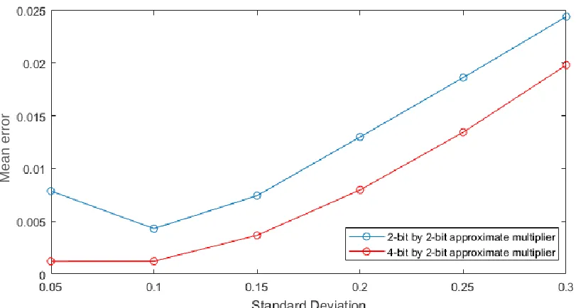
Figure 9: Simulated mean error for varying normal distributions in a 8x8 multiplier built from ax2x2 or ax4x2 multipliers
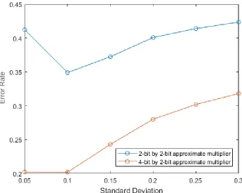
In Figure 9, the average relative error can be seen for both approximate multiplier designs in 8x8 multipliers for normal distributions with varying standard deviations. The distributions all have their centre in the middle of the input range and have any values outside the range clipped back to the edges of the range.
The higher error for the SD=0.05 distribution for the Ax2x2 design is caused by the fact that the strong concentration of inputs around ‘00111111’ cause a lot of errors in the Ax2x2 design while the 4bit by 2-bit design is less susceptible to this. This can also be seen in Figure 10 10, which shows the error rate (ER), defined by 𝑒𝑟𝑟𝑜𝑟 𝑐𝑎𝑠𝑒𝑠
𝑡𝑜𝑡𝑎𝑙 𝑜𝑝𝑒𝑟𝑎𝑡𝑖𝑜𝑛𝑠, for the different normal distributions.
Me
an
err
15 Figure 10: Error rate for varying normal distributions
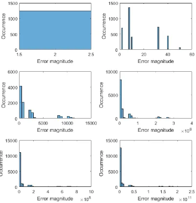
Figure 11: Relative average error and occurrence of errors for varying bit-widths (2x2, 4x4, 8x8, 12x12, 16x16 and 20x20) and a uniform input distribution
E
rr
or
R
ate
E
rr
or
R
ate
M
ea
n
E
rr
[image:15.612.127.470.407.684.2]16 Figure 11 shows the average relative error and the occurrence of errors for varying bit widths under a uniform input distribution. These confirm the trend noticed in Kulkarni’s paper, where the average relative error increases when the bit width of the multiplier is increased, but levels out at higher bit widths. This is due to the relative decrease of large errors, as shown in the histograms or errors in Figure 12. This relative decrease was expected from the error maps discussed in the previous subsection on the mathematical analysis, where the occurrence of smaller errors also increased relatively to the larger errors. The 4x2 multiplier behaves similarly to the 2x2 design for increasing bit-widths and is therefore not shown.
17
Testing setup
Originally the assignment had an 8-bit by 8-bit multiplier with an accumulator as its design specification. In later stages of the research, focus shifted to the multiplication and the accumulator was left out so that the multiplier could be examined better.
The multiplication is done through partial product generation with smaller multipliers. 4
variations of these multipliers were tested, in addition to the default multiply operation in VHDL: (a) the 2-bit by 2-bit accurate multiplier, (b) the 2-bit by 2-bit approximate multiplier, (c) the 4-bit by 2-bit accurate multiplier and (d) the 4-bit by 2-bit approximate multiplier.
The generated partial products must be shifted and added to arrive at the final product. The variations that were tested for this were (a) simple shift and add, (b) rearranged shift and add and (c) Wallace tree adding. With Wallace tree adding, the accumulation was integrated in the addition of the partial products.
The combinations of these designs will then be compared in their size (LE/ALM count), power consumption and accuracy.
Multipliers
The reference design simply used the multiply operation (‘*’). The logic for the partial multipliers was designed using Karnaugh maps for every output bit, which were then parsed through a converter to receive the bit-level logic that could be used in VHDL. [6] The truth tables and the bit-level logic can be found in the Appendix. Gate diagrams were omitted as the gate-level architecture is not relevant with the LUT-based functioning of FPGA’s.
Tuneable error
The accurate and approximate partial multipliers can be combined in a multiplier block to trade off accuracy for synthesis area and power consumption. The multiplier built out of 2x2 partial multipliers uses 16 partial multipliers, while the multiplier built out of 4x2multipliers uses 8. When replacing accurate multipliers for their approximate counterparts, it is most efficient to start with the multipliers tasked with the lowest order, as any errors that will be generated will also be of a lower order, while still achieving the same power and size savings as replacing another partial multiplier would give.
Several mixed multipliers were made with each design to be able to effectively compare the two designs.
Adder structures
In the simple shift and add structure, each partial product is concatenated with the correct amount of zero bits, resulting in a width of 16 bits for each product, and all products are then added simultaneously with the + operator.
18
Test bench and input data
In order to test the performance of the MAC designs, a test bench was written, which supplied input data, collected output data and sent control signals to the accumulator. Input data,
consisting of a multiplier and a multiplicand, were randomly generated with a Matlab script, in a uniform and several normal distributions. All input data was distributed in the range 0-255, with the tails of the distribution clipped to the end values of this range. The mean was set at 127,5 and standard deviations, shown as 0,1-0,3 are relative to the whole range. This input data was supplemented in Matlab with several control signals for the VHDL testbench: a “write” signal for the output and a “reset” signal for the accumulator, which were used to signal the end of an accumulator set. Every clock cycle one line of these inputs was then read by the test bench.
Timing and critical path length
When the functional code has been written in VHDL and functionally verified in Modelsim, the code is synthesized in Quartus to acquire a hardware architecture. Quartus maps out which logic elements need to perform what function and routes the logic elements together in an appropriate way. With this architecture, timing information becomes available, which can then be used to perform post-synthesis simulation in Modelsim. It is in this stage that any timing issues come to the surface.
To make the post-synthesis model compatible with the timing independent test bench, inputs and outputs are communicated through registers.
Performing both the partial product generation and the addition operations in a single clock cycle proved to be difficult, especially because of the large critical path of the adder tree.
Therefore, the two operations are carried out in two separate clock cycles. This does not have a large influence on performance however, as the two operations are pipelined, i.e. the partial multipliers can already start on the next inputs, while the adder finishes up the previous inputs. This does however still create a small extra delay in the first calculation.
Power analysis and size metrics
19
4. Results
The reference 2-bit by 2-bit design and the new 4-bit by 2-bit design were tested by synthesizing them, performing a post synthesis simulation with 10,000 pairs of input data and running the value change dump generated by this simulation in a power analysis. This simulated power consumption consisted out of 3 parts: the static consumption, dynamic consumption and a part that was used for IO pins. As only the dynamic power consumption was relevant for comparison between the multiplier designs, this was the metric used for results.
Approximate multiplier designs
The error displayed is the earlier mentioned average relative error, obtained by taking the average of all relative errors for the given input distribution.
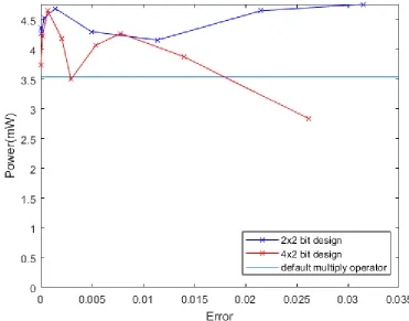
[image:19.612.114.485.346.637.2]Figure 13 shows the power consumption compared to the accuracy for the mixed multiplier designs in Cyclone IV LE architecture. The additions of the partial products are done with shifting and adding for all these designs. The 4x2 design mostly outperforms the 2x2 design but is only more power efficient than the default multiply operation when all 8 partial multipliers are of the approximate design. Furthermore, the power consumption does not follow a predictable trend. This is probably due to differences in routing efficiency.
Figure 13: Power consumption for uniform input distribution versus error in an 8x8 multiplier
20 In Figure 14 the size of the multiplier designs can be seen versus their accuracy. As said before, the 4-bit by 2-bit design performs better for narrower input distributions. The sizes of the designs are constant, but due to this difference in accuracy for these distributions, the 4-bit by 2-bit design outperforms the 2-bit by 2-bit design at all accuracies for a normal distribution with a standard deviation of 0.1.
Figure 14: Size in Logic Elements in Quartus IV architecture versus accuracy of designs in 8x8 multipliers
Since the 4-bit by 2-bit design was made for the Cyclone V ALM architecture, it is surprising that it can outperform the 2-bit by 2-bit design in power consumption and is competitive in size. It is unlikely that this is attributable to its design and more likely that the freedom that Quartus got with realizing the design, caused it to optimize it.
21 Figure 15: Size in Advanced Logic Modules in Quartus V architecture versus accuracy of designs
To see whether the size results for the Cyclone V designs might give an indication for the power usage, the size and power results of the Cyclone IV designs were compared in
Figure 16. There seems to be no clear trend between size and power, so it can be assumed that the power consumption is more dependent on the actual switching activities than on the size of the design. Therefore, power performance in Cyclone V of the designs is not possible to measure, except for an actual power measurement on a running FPGA board.
Adder designs
Early in the design cycle, the Wallace tree design was already found out to be inefficient on FPGA. This is because the Wallace tree is built up out of full- and half-adders, which do not translate well in FPGA architecture. If some additional control over the carry lines is possible, this might still be a viable adding technique though, as demonstrated in [7].
22 Figure 16: Power versus size for Cyclone IV designs
Figure 17Power consumption for different adder designs in an 8x8 multiplier Area (LE)
P
ower
(mW
23 Figure 18: Size in Cyclone IV for the two adder designs in an 8x8 multiplier
[image:23.612.114.477.409.702.2]24
5. Discussion and recommendations
Unfortunately, the results of the measurements do not reflect the expected improvements from the theory. In this chapter, several factors will be discussed which might have played a part in this.
Lack of synthesis control
The 4-bit by 2-bit design is designed to make maximum use of the ALM architecture. When looking at net-lists, it did not seem that the ALM’s were being utilised in the designed method. It might be possible that programming in VHDL primitives might give more control in these low-level functions, but this was beyond the scope of this work. The unexpected mapping might also be caused by routing difficulties, as the designs did not take routing or timing in consideration.
Synthesis optimization
The designs for the multipliers and the adders contain a lot of low-level functions which assign operations on the bit level. This may have interfered with the optimization that Quartus performs during synthesis, reducing the predicted gains that the new designs should have delivered.
Synthesis unpredictability
At certain times, synthesis of the VHDL designs proved to be unpredictable, resulting in different synthesis results for the same files. These different results have had timing issues, where the previous synthesis result had none. They also caused more basic problems, like unsigned ports which were suddenly differently synthesized as std_logic_vectors.
Routing complexity
During post-synthesis simulation, many designs were found to have timing issues. Many of these were resolved, but for several designs this was not possible. Due to the high complexity of the designs after synthesis, it was not possible to find the cause of these issues. They did not seem to be singularly dependent on specific design choices as some combinations had timing issues, while each of the chosen design options were present in other designs which did not present timing issues.
Post synthesis simulation complexity
The post synthesis simulations were very time-consuming operations, with the 10,000 input test sets costing up to 20 minutes of real time to run. This made it unfeasible to run the power analyses for all the input distributions. The metric that has now been used for comparison, LE size or ALM size, is a poor predictor for power consumption.
Recommendations
Since the 4-bit by 2-bit design unexpectedly outperformed the default multiplying operation in the Cyclone IV test with uniformly distributed inputs, there seems to be room for optimization in multiplying operations since this design was not even designed to be efficient on this
25
6. Conclusion
The proposed addition scheme featuring rearrangement of partial products before addition performed well, compared to simple shifting and adding, giving better results in both size and power consumption and performing better when there was a large amount of terms to be added that have been bit shifted a significant number of bits relative to each other.
It was not possible to realise the expected size or power consumption gains with approximate multiplication schemes on FPGA. Both the 2-bit by 2-bit design and the 4-bit by 2-bit design had synthesis sizes larger than the default multiplier operation in Cyclone IV. In Cyclone V, the 4-bit by 2-bit design was not able to decisively outperform the 2-bit by 2-bit design in size and although this does not mean power consumption has to be worse as well, the larger than expected size means it’s likely the optimised design was not synthesised as expected.
Although similar compression algorithms have been used on FPGA by others, showing that it is possible to use compression trees in FPGA, the Wallace tree was not able to be realised efficiently in this research.
The disappointing results might be caused by complications in routing and mapping, which were not considered in the designs, or an insufficient amount of knowledge on the synthesis
26
Appendix: Approximate multiplier designs
c1c0
b1b0 00 01 11 10
00 0000 0000 0000 0000
01 0000 0001 0011 0010
11 0000 0011 1001 0110
10 0000 0010 0110 0100
Appendix 1: Accurate 2-bit by 2-bit multiplier K-map and bit logic
a(0)<=b(0)AND c(0);
a(1)<=(NOT(b(1)) AND b(0) AND c(1)) OR
(b(0) AND c(1) AND NOT(c(0))) OR
(b(1) AND NOT(b(0)) AND c(0)) OR
(b(1) AND NOT(c(1)) AND c(0));
a(2)<=(b(1) AND not(b(0)) and c(1)) OR
(b(1) AND c(1) AND NOT(c(0)));
a(3)<=b(1) AND b(0) AND c(1) AND c(0);
B1B0
A1A0 00 01 11 10
00 000 000 000 000
01 000 001 011 010
11 000 011 111 110
10 000 010 110 100
a(0)<=b(0)AND c(0);
a(1)<=(b(0)AND c(1))OR
(b(1) AND c(0));
a(2)<=b(1) AND c(1);
27 c1c0
b3b2b1b0 00 01 11 10
0000 000000 000000 000000 000000
0001 000000 000001 000011 000010
0011 000000 000011 001001 000110
0010 000000 000010 000110 000100
0110 000000 000110 010010 001100
0111 000000 000111 010101 001110
0101 000000 000101 001111 001010
0100 000000 000100 001100 001000
1100 000000 001100 100100 011000
1101 000000 001101 100111 011010
1111 000000 001111 101101 011110
1110 000000 001110 101010 011100
1010 000000 001010 011110 010100
1011 000000 001011 100001 010110
1001 000000 001001 011011 010010
1000 000000 001000 011000 010000
a(0)<=b(0)AND c(0);
a(1)<= (not(b(1)) AND b(0) AND c(1) ) OR
( b(0) AND c(1) AND not(c(0)) ) OR
( b(1) AND not(b(0)) AND c(0) ) OR
( b(1) AND not(c(1)) AND c(0));
a(2)<= (not(b(1)) AND b(0) AND c(2) ) OR
( b(0) AND c(2) AND not(c(1)) ) OR
( b(0) AND c(2) AND c(0) ) OR
( b(1) AND not(b(0)) AND c(1) ) OR
( b(1) AND not(c(2)) AND c(1) AND not(c(0)));
28
( b(1) AND not(b(0)) AND c(2) ) OR
( b(0) AND c(3) AND not(c(2)) AND not(c(1)) ) OR
( b(0) AND c(3) AND not(c(2)) AND not(c(0)) ) OR
( b(0) AND c(3) AND c(2) AND c(1) ) OR
( b(1) AND not(c(3)) AND c(2) AND not(c(1)) ) OR
( b(1) AND b(0) AND not(c(3)) AND not(c(2)) AND c(1) AND c(0));
a(4)<= (b(1) AND not(b(0)) AND c(3)) OR
( b(1) AND not(c(1)) AND c(3) AND not(c(2)) ) OR
( b(1) AND c(3) AND not(c(2)) AND not(c(0)) ) OR
( b(1) AND b(0) AND not(c(3)) AND c(2) AND c(1) );
a(5)<= (b(1) AND b(0) AND c(3) AND c(2)) OR
( b(1) AND b(0) AND c(3) AND c(1) AND c(0));
Appendix 3: Accurate 4-bit by 2-bit multiplier K-map and bit logic.
c1c0
b3b2b1b0 00 01 11 10
0000 00000 00000 00000 00000
0001 00000 00001 00011 00010
0011 00000 00011 01001 00110
0010 00000 00010 00110 00100
0110 00000 00110 10010 01100
0111 00000 00111 10101 01110
0101 00000 00101 01111 01010
0100 00000 00100 11111 01000
1100 00000 01100 11111 11000
1101 00000 01101 11111 11010
1111 00000 01111 11111 11110
1110 00000 01110 11111 11100
1010 00000 01010 11110 10100
1011 00000 01011 11111 10110
29
1000 00000 01000 11000 10000
a(0)<= (b(0) AND c(0)) OR (b(1) AND b(0) AND c(3) AND c(2));
a(1)<= (NOT(b(1)) AND b(0) AND c(1))
OR (b(0) AND c(1) AND NOT(c(0)))
OR (b(0) AND c(3) AND c(1))
OR (b(1) AND NOT(b(0)) AND c(0))
OR (b(1) AND NOT(c(1)) AND c(0))
OR (b(1) AND b(0) AND c(3) AND c(2));
a(2)<= (NOT(b(1)) AND b(0) AND c(2))
OR (b(0) AND c(2) AND NOT(c(1)))
OR (b(0) AND c(2) AND c(0))
OR (b(1) AND NOT(b(0)) AND c(1))
OR (b(1) AND c(3) AND c(1))
OR (b(1) AND NOT(c(2)) AND c(1) AND NOT(c(0)));
a(3)<= (b(0) AND c(3))
OR (b(1) AND NOT(b(0)) AND c(2))
OR (b(1) AND c(2) AND NOT(c(1)))
OR (b(1) AND b(0) AND NOT(c(2)) AND c(1) AND c(0));
a(4)<= (b(1) AND c(3))
OR (b(1) AND b(0) AND c(2) AND c(1));
30
References
[1] P. G. M. E. Parag Kulkarni, “Trading Accuracy for Power with an Underdesigned,” 2011. [2] C. Wallace, “A Suggestion for a Fast Multiplier,” IEEE Transactions on Electronic
Computers, 1964.
[3] S. A. a. P. Z. Martin Kumm, “An Efficient Softcore Multiplier Architecture for Xilinx FPGAs,”
2015 IEEE 22nd Symposium on Computer Arithmetic, 2015. [4] “Altera White Paper on ALM architecture,” 2006. [Online]. Available:
https://www.intel.com/content/dam/www/programmable/us/en/pdfs/literature/wp/wp-01003.pdf.
[5] HADI PARANDEH-AFSHAR, “Compressor Tree Synthesis on Commercial
High-Performance FPGAs,” ACM Transactions on Reconfigurable Technology and Systems, vol. 4, no. 4, 2011.
[6] “http://www.32x8.com/,” [Online].
[7] H. N. A. B. P. a. I. P. Parandeh-Afshar, “An Efficient Softcore Multiplier Architecture for Xilinx FPGAs”.
List of figures
Figure 1: Shift and add multiplication ... 5
Figure 2: 2-bit by 2-bit multiplier [1] Figure 3: Combining 2-bit by 2-bit multipliers ... 5
Figure 4: The accurate multiplier on the left and the approximate version on the right [1] ... 6
Figure 5: Adaptive Logic Element architecture [3] ... 7
Figure 6: Comparison theoretical resource usage partial multipliers ... 9
Figure 7: Left the normal shift and add structure, right the rearranged structure...10
Figure 8: Simulated average relative error for varying normal distributions ...14
Figure 9: Occurrence of errors for varying normal distributions ...15
Figure 10: Relative average error and occurrence of errors for varying bit-widths ...15
Figure 11: Distribution of occurrences of different error magnitudes for a 2-bit by 2-bit approximate multiplier, combined for increasing bit widths (namely for 2, 4, 8, 12, 16 and 20 bit inputs respectively from left to right, top to bottom) ...16
Figure 12: Power consumption for uniform input distribution versus error ...19
Figure 13: Size in Logic Elements in Quartus IV architecture versus accuracy of designs ...20
Figure 14: Size in Advanced Logic Modules in Quartus V architecture versus accuracy of designs ...21
Figure 15: Power versus size for Cyclone IV designs ...22
Figure 16Power consumption for different adder designs ...22
![Figure 4: The accurate multiplier on the left and the approximate version on the right [1]](https://thumb-us.123doks.com/thumbv2/123dok_us/9695529.470839/6.612.87.528.515.677/figure-accurate-multiplier-left-approximate-version-right.webp)
![Figure 5: Adaptive Logic Element architecture [3]](https://thumb-us.123doks.com/thumbv2/123dok_us/9695529.470839/7.612.130.492.260.432/figure-adaptive-logic-element-architecture.webp)