Abstract— An anomalous current observed in reverse-biased pn junctions, highly-integrated with an extremely small cells, is analyzed with the help of device simulation. At the tail of the appearance probability, junction currents showed a steep increase and saturation as a function of applied bias.
A model of localized deep-traps is proposed to explain the anomaly. The deep traps are formulated as a g/r center based on the Shockley–Read–Hall model. Simulation results clarify the mechanism of the current anomaly: when deep traps are included in the depletion layer, they act as a carrier generation center and the junction current steeply increases. The magnitude of the current after saturation is discussed, focusing on capture rate and trap density. Further, experimental features for the anomaly, e.g., the fluctuation in the critical voltage at which the current begins to increase and the structure dependence of the anomalous current, are also discussed using the present deep-trap model.
I. INTRODUCTION
C
ARRIER lifetimes in semiconductors are important in-dicators [1] of material quality and process cleanliness. The carrier generation-recombination assisted by single level traps is a fundamental process in determining the lifetime. This process was originally studied by Shockley–Read [2] and Hall [3], and the basic theory is well known as the SRH model. Based on the SRH model, the multilevel, field-strength, and temperature dependence have been studied [4]–[6] and the device operation mechanism has been analyzed [7], [8].The current component associated with traps frequently leads to deterioration in device performance. For example, the current gain in bipolar transistors is degraded by surface recombinations [9]. And the data retention time of DRAM’s is shortened by the leakage current in pn junctions [10]. Further, an anomalous behavior has been observed in current–voltage ( ) characteristics of a CCD gated-diode structure [11].
Recently, semiconductor device dimensions have been dras-tically minimized to achieve high-speed and low-power oper-ations. When active currents or charges are scaled-down for achieving low-power operation, damage due to the current component associated with traps is relatively increased against the normal device action.
Manuscript received July 6, 1998. The review of this paper was arranged by Editor A. H. Marshak.
K. Yamaguchi and T. Teshima are with the Central Research Laboratory, Hitachi Ltd., Tokyo 185, Japan.
H. Mizuta was with the Central Research Laboratory, Hitachi Ltd., Tokyo 185, Japan. He is now with Hitachi Cambridge Laboratory, Cambridge CB3 0HE, U.K.
Publisher Item Identifier S 0018-9383(99)04592-X.
[image:1.612.307.555.197.355.2](a) (b)
Fig. 1. Retention time of DRAM memory cells with small dimensions and leakage current flowing through pn junctions under reverse-biased conditions (after Ogasawara et al. [12]): (a) cumulative failure versus logarithmic retention time and (b)I0V characteristics observed in the tail distribution shown in (a).
The recent memory cell-size of DRAM’s is in the order of a submicron squared area. The leakage current flowing through pn junctions in these memory cells is a key factor which determines the data retention time. The aim of this paper is to study the anomalous current observed in small-dimension pn junctions [12], i.e., an unexpectedly high leakage current which makes the retention time extremely short. A locally generated deep-trap model is proposed to explain the anomaly in characteristics. Based on this model, the mechanism that induces the anomaly is analyzed with the help of a one-dimensional (1-D) simulation. A structure dependence of the anomalous current is also analyzed using a two-dimensional (2-D) numerical simulation. Quantitative evaluations will be given from the viewpoint of the material constants, particula, focused on the capture rate and trap density which determine carrier lifetimes.
II. ANOMALOUSBEHAVIOR IN PN-JUNCTION
CURRENT AND CARRIERTRANSPORTMODELING
Measured retention times for DRAM’s are scattered in a finite range, and the frequency of appearance is usually plotted as cumulative probability versus logarithmic retention time. As schematically shown in Fig. 1(a), the cumulative distribution consists of two parts: the main distribution (given by the straight line) and the tail. The retention time in systems is
1160 IEEE TRANSACTIONS ON ELECTRON DEVICES, VOL. 46, NO. 6, JUNE 1999
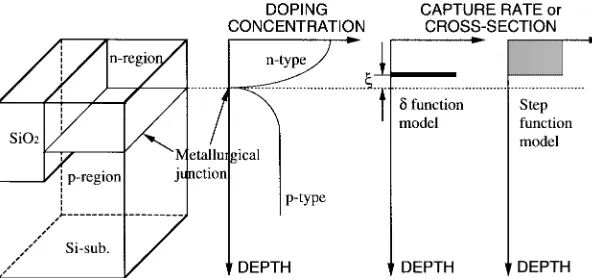
Fig. 2. Proposed deep-trap model: (a) analyzed device structure, (b) doping profile, (c) delta-function-type deep-trap model, and (d) step-function-type deep-trap model.
determined by the shortest time in the distribution. Thus, the existence of the short retention time in the tail distribution is a serious problem for developing high-density LSI’s.
In the tail bit, an anomalous behavior has been reported [12]; that is, – characteristics showed a steep increase and saturation as illustrated in Fig. 1(b). The steep increase in – curves is hereafter called the jump in current or the current-jump. In this jump, the current increases stepwise and, consequently, the data retention time is shortened. The saturation level after the jump exceeds that of nonanomalous levels by a factor of 10 to 10 .
Jumping phenomena have already been observed in semi-insulating GaAs substrates [13], [14]. A theoretical study [14] has reported a current component assisted by deep traps in an n-i-n structure, where electrons are injected from an n to an i-layer. In pn junctions under the reverse bias condition, however, electrons cannot be injected anywhere. A new model explaining the step mechanism in – curves is discussed in the last part of this section.
The carrier transport including trap-assisted components can be phenomenologically modeled using the current continuity equation
(1)
and
(2)
Here, is the generation/recombination rate given by
(3)
is the g/r rate given by the SRH model. And and are the g/r rates from deep donor- and acceptor-type traps, and they can be modeled as follows:
(4)
and
(5)
Here, and are the deep donor and acceptor densities, and and are the electron and hole capture rates.
Parameters and in (4) and (5) are given by
(6)
and
(7)
Here, is the energy level of the deep trap center. The functional formulas of and are commonly used for deep donors and acceptors. However, the energy level and the capture rates are individually defined for deep donors and acceptors.
Poisson’s equation which determines the potential distribu-tion can be written as
(8)
The space charges that originate in ionized donors and ac-ceptors, i.e., and , consist of the shallow and deep ones. The space charge densities generated from deep traps are calculated as
(9)
and
(10)
The above deep-trap modeling had been traditionally used in analyses of compound semiconductor devices [8], [14], [15].
Fig. 3. Current–voltage characteristics and depletion layer width analyzed by 1-D device simulation to the depth direction. In the numerical scheme, the deep trap is set at one mesh point for representing the delta-function and the trap density at this point is assumed to be 1018 cm03. The energy level of deep traps is also assumed to be at the mid-gap, the capture rates,Cn and
Cp, to be 1008 cm3/s, and the lifetime of bulk Si to be 1006s.
changed one; namely, a step-function model as illustrated in Fig. 2(d).
III. ANOMALOUS BEHAVIOR ANALYSIS
For simplicity, donor-type traps distributed like a delta-function are assumed and the energy level is set at the
middle of the energy gap ( eV). The
delta-function is modeled by setting the deep trap at one mesh point in a numerical scheme. Current–voltage characteristics are calculated by 1-D simulation to the depth direction and results are given in Fig. 3. The depletion layer width obtained from simulation is also given in the figure.
As seen in the figure, the depletion layer is widened with an increase in the applied bias. When the edge of the depletion layer reaches the position where the deep traps are located, the current flowing through the pn junction steeply increases. That is, when deep traps are included in the depletion layer, the deep traps make the electrical state active. Consequently, carriers assisted by deep traps are emitted into the depletion layer and the junction current steeply increases. If the deep trap model is ignored, the current-jump is not found.
When a high bias is applied and the depletion layer expands over the trap-generated location, the deep traps are completely activated. Thus, the junction current is saturated in the high-bias region. This is the physical mechanism of the current-jump and saturation.
[image:3.612.320.540.60.261.2]A steep increase and saturation in characteristics in semi-insulating GaAs with an n-i-n structure originates in the quasi-Fermi potential pinning at the deep-trap level and in the depinning caused by the carrier injection from the n region [14]. However, in reverse-biased pn junctions, carriers cannot be supplied from an n or p region. Deep traps in the depletion layer behave as a carrier-supplier and generated carriers steeply increase the junction current.
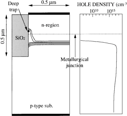
Fig. 4. Hole distribution analyzed by 2-D simulation: (a) contour map of the hole density distribution where deep traps behave like a carrier source and (b) hole density distribution along the righthand side-wall in (a).
Electrical behavior of deep traps as a carrier-generation center can be understood using carrier distribution maps. By carrying out 2-D simulation, the hole distribution is analyzed and results are illustrated using a contour map as shown in Fig. 4. In the present analysis, deep traps are set by the delta-function model at the Si/SiO interface (see the closed circle in the figure) and the Si/SiO interface except for the tarp-generated region is assumed to be clean. It is found that holes are emitted from the trap center situated in the n region and flow toward the p region.
The expansion of the depletion-layer width, especially in the n-region, is not smooth but rather pinned, while the depletion-layer edge in the p-region smoothly expands according to the square root of the applied bias. When the depletion region edge reaches the trap-generated location, deep traps are ionized as described in (9). Thus, the space charge density varies even if the depletion layer edge is spatially fixed. This is the reason for the depletion layer pinning shown in Fig. 3.
As described above, the current-jump occurs when the deep traps are included in the depletion layer. Thus, it is inferred that the critical voltage, , above which the current steeply increases depends on the location of the deep traps. Current–density versus voltage characteristics are calculated and the results are shown in Fig. 5. Calculations are carried out assuming several sets of the distance, , between the metallurgical junction and the trap-localized portion. The critical voltage is varied by changing . Experimentally, it is scattered in a range of a few volts. From the present analysis, it is found that the fluctuation of the trap generation in a range of 0.05 m induces the experimentally observed fluctuation
in .
middle-1162 IEEE TRANSACTIONS ON ELECTRON DEVICES, VOL. 46, NO. 6, JUNE 1999
[image:4.612.355.511.58.188.2]Fig. 5. Calculated current–voltage characteristics for various distances between the trap-generated position and the metallurgical junction given in Fig. 2. Material constants used in this analysis are identical with those used in Fig. 3.
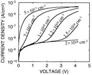
Fig. 6. Calculated current–voltage characteristics for various doping levels as a parameter. Material constants used in this analysis are identical with those used in Fig. 3.
level in the doping concentration is varied and the doping level of 1 10 cm is selected as a reference point. When the doping level is fluctuating 50% around the reference point, the fluctuation in is in a range of a few volts. Thus, the sensitively changes with a change in the doping level.
IV. INTERFACE TRAP ANALYSIS
[image:4.612.89.249.298.428.2]In this section, the device operation assisted by interface traps is analyzed using 2-D simulation. Assuming deep traps at the Si/SiO interface as illustrated in Fig. 4(a), anomalies of the junction current, especially on the structural dependence of the anomalous current, are analyzed. The Si/SiO interface except for the trap-generated portion is assumed to be clean. As shown in Fig. 7, a steep increase and saturation in currents are demonstrated in 2-D simulation. The low-level current before the current-jump linearly depends on the junction area, namely, the current is caused by the bulk g/r center. Contrary, the high-level current in the saturation region induced by interface traps is independent of the junction area. In the 2-D analysis, the potential and carrier distributions are assumed to be uniform in the third axis perpendicular to the analyzed plane. Consequently, the magnitude of currents induced by
Fig. 7. Device-structural dependence analysis of anomalous current with the help of 2-D simulation. The cross section analyzed here is analogous to the structure shown in Fig. 4(a). The width of the pn junction in this cross section is assumed to be 0.2, 0.4, and 0.8m for devices #1–3, respectively. The parameter,S, inserted in the figure denotes the relative area of pn junctions whenS for device #1 is assumed to be unity (a.u.) as a reference.
the interface trap is linearly dependent on the perimeter. The validity of the model is discussed by comparing simulation results to experimental data in a later section.
In the previous analysis, the spatial distribution of deep traps is assumed to be a delta-function both in 1-D and 2-D simulation, and the current-jump and saturation mechanisms were analyzed. When the step-function model shown in Fig. 2(d) is assumed, the current-jump and saturation can also be obtained from simulation. The current-jump is caused by electrically activated deep traps and the saturation current level is determined linearly depending on the interface trap density. The anomaly mechanism in small-size pn junctions can be successfully analyzed using the proposed deep-trap model.
V. HIGH FIELD EFFECT
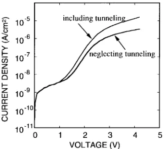
As can be seen in Fig. 1(b), the measured differential-conductance in the high-current-saturation region is over a few volts per decade on a semilogarithmic scale, although the calculated conductance is low as shown in Figs. 5–7. The measured high-conductance is guessed to be caused by tunneling-enhanced emission of electrons from traps [7] under the high-field condition.
Trap-assisted tunneling can be modeled using the field dependent capture rate [7], [11] and functional formulas are given by
(11)
and
(12)
Here, is the electric field, is the zero-field capture rate, and is a field-independent parameter calculated from material constants.
Fig. 8. Calculated current–voltage characteristics including trap-assisted tunneling or neglecting it.
VI. MAGNITUDE OF CURRENT ANDMATERIALCONSTANTS
Focused on the low- and high-level currents, and , given in Fig. 1(b), simulation results are compared with experimental data and the validity of the present model is quantitatively evaluated. First, the low level current, , is analyzed using the following two models; namely, the bulk-type g/r model and the interface trap model.
Assuming the bulk-type g/r model, the recombination
life-time, , is obtained from ( , where is the
trap density. The generation lifetime, , under reverse-biased
conditions is defined by due to
and is given by a function of , and [16]. In
simulation, the carrier densities, and , are obtained by solving the current continuity equations and the operation of , namely, acts as the recombination or generation process, is determined depending on the carrier densities. For simplifying the evaluation, simulation results are plotted as a function of .
Results are shown in Fig. 9(a), where the current density obtained from 1-D simulation is translated to the current as-suming the junction aria of (0.5 m) . Lifetimes for electrons and holes are assumed to be equal for simplicity. As shown in the figure, the calculated current is inversely proportional to the lifetime. The measured current is less than 10 A at room temperature. From this analysis, the lifetime is estimated to be around 10 s. This is smaller than conventionally known lifetimes [1].
Next, the trap model is evaluated, where interface-traps are assumed to be uniformly distributed at the hatched area in the insertion in Fig. 9(b) and 2-D simulation is carried out. Results are given as a function of the interface trap density, where the capture rates for electrons and holes are equal for simplicity. Assuming cm /s, simulation results indicate that the interface trap density is in the order of 10 cm . This value is in an experimentally reasonable range. Further, it is experimentally known that the magnitude of currents flowing through small pn junctions depends on the perimeter rather than the area size. As described previously, the magnitude of currents obtained from 2-D simulation is linearly dependent on the perimeter. Thus the interface trap is a candidate which determines the low level current.
[image:5.612.88.252.58.205.2](a) (b)
[image:5.612.352.511.305.435.2]Fig. 9. Low-level current (IL) analysis. Simulation results are denoted by the solid line: (a) assuming bulk g/r model,IL is calculated as a function of lifetime by 1-D simulation. Current levels obtained from experiments are shown by the arrow and (b) assuming interface trap model, ILis also calculated as a function of the interface trap density by 2-D simulation. The pn junction area is assumed to be (0.5m)2both in (a) and (b).
Fig. 10. High-level current (IH) analysis as a function of capture rate. Two-dimensional simulation results are denoted by the solid line and measured current levels are indicated by the shadowed area. As schematically illustrated in the insertion, deep traps are generated at the Si/SiO2interface using the delta-function model and the trap density is set at1 2 1012cm02along the bold line. The total number of deep traps corresponds to 50 in the analyzed volume when the pn junction area is assumed to be (0.5m)2. Capture rates for electrons and holes are assumed to be equal for simplicity.
Finally, the high-level current, given in Fig. 1(b), is analyzed assuming the device structure inserted in Fig. 10. Deep traps are spatially localized like a delta-function and the interface between Si/SiO except for the localized trap center
is assumed to be clean. When is assumed
in (4) and (5), the g/r rate assisted by deep traps linearly depends on the product. As described previously, locally generated deep traps are modeled by the changing capture rate. In this section, the current, , is evaluated as a function of the capture rate, , with fixed .
High-level currents are calculated and results are shown in Fig. 10, where 50 traps are generated in the analyzed volume by setting the interface trap density to cm along the dark area in the insertion. When the calculated is compared to experimental values, the capture rate is estimated to be 10 cm /s or less. The capture rate calculated from the capture cross section, , is estimated to be and
1164 IEEE TRANSACTIONS ON ELECTRON DEVICES, VOL. 46, NO. 6, JUNE 1999
and cm [1]). For Au in Si [17], and
are in a range of to cm (i.e.,
to cm /s). The capture rate estimated from under the assumption of 50 traps in a cell exceeds that obtained from by a factor of 10–10 .
On the contrary, if cm /s is assumed, the
total number of deep traps is estimated to be around 10 . It was experimentally estimated that Fe ions in initial as-grown crystals are contained in the range of 10 –10 cm . An Si substrate with a 100 m thickness contains 10 –10 Fe atoms/cm . The anomalous behavior has been experimentally observed at the appearance probability of 10 , when an extremely small pn junctions are integrated with an ultrahigh density. When a (0.5 m) pn junction is integrated with isolated regions, cells can be fabricated on a unit area (1 cm ) and therefore anomalous currents would be found in 50 cells. In this case, the trap density is from 10 to 10 cm . This is not unrealistic considering the number of Fe-ions in the substrate. Actually, heavy implantations, for example, around 10 cm or 50 keV, were used during highly integrated LSI fabrication. Thus, implantation defects or heavy metal contamination might be induced near the metallurgical junction.
Deep traps are a candidate for origins that induce the anomalous behavior observed in the tail distribution shown in Fig. 1(a). In fact, temperature-dependent transport measure-ments have shown that activation energies situated near the middle of the energy gap [12]. However, it is very difficult to detect such low-density traps because the detection limit of current equipment, e.g., total reflection X-ray fluorescence, is in the order of 10 cm . Further research is required for determining the origin of the anomaly.
VII. CONCLUSIONS
When the size of pn junctions is shrunk and junction cells are largely integrated with an ultra-high density, an anomalous current is observed in the tail of the cumulative distribution. Junction currents frequently show a steep increase and satu-ration under reverse-biased conditions. Such an anomaly has been analyzed by device simulation.
A locally generated deep-trap model is proposed as an origin of the anomaly. Based on the proposed model, the mechanism of the anomaly and the structure dependence of the anomalous current are studied. The magnitude of currents after the saturation is analyzed as a function of the capture rate and trap density. Results from device simulation are compared to experimental data, and the trap density is estimated considering the frequency of appearance for the anomalous currents.
ACKNOWLEDGMENT
The authors wish to thank Dr. Y. Tadaki, Dr. M. Ogasawara, Dr. S. Kimura, Dr. A. Hiraiwa, Dr. S. Ooyu, Dr. M. Horiuchi, Dr. S. Isomae, and Dr. T. Itoga for their valuable discussions during this work.
REFERENCES
[1] D. K. Schroder, ”Carrier lifetimes in silicon,” IEEE Trans. Electron
Devices, vol. 44, pp. 160–170, Jan. 1997.
[2] W. Shockley and W. T. Read, “Statistics of recombinations of holes and electrons,” Phys. Rev., vol. 87, pp. 835–842, Sept. 1952.
[3] R. N. Hall, “Electron-hole recombination in germanium,” Phys. Rev., vol. 87, p. 387, July 1952.
[4] A. Schenk and U. Krumbein, “Coupled defect-level recombination: Theory and application to anomalous diode characteristics,” J. Appl.
Phys., vol. 78, no. 5, pp. 3185–3192, Sept. 1995.
[5] A. Schenk, “A model for the field and temperature dependence of Shockley–Read–Hall lifetimes in silicon,” Solid-State Electron., vol. 35, no. 11, pp. 1585–1596, 1992.
[6] A. Schenk, “An improved approach to the Shockley–Read–Hall recom-bination in inhomogeneous fields of space-charge regions,” J. Appl.
Phys., vol. 71, no. 7, pp. 3339–3349, Apr. 1992.
[7] G. A. M. Hurkx, D. B. M. Klaassen, and M. P. G. Knuners, “A new recombination model for device simulation including tunneling,” IEEE
Trans. Electron Devices, vol. 39, pp. 331–338, Feb. 1992.
[8] S. Ho, M. Oohira, O. Kagaya, A. Moriyoshi, H. Mizuta, and K. Yamaguchi, “Dynamic simulation of multiple trapping processes and anomalous frequency dependence in GaAs MESFET’s,” IEICE Trans.
Electron., vol. E77-C, no. 2, pp. 187–193, Feb. 1994.
[9] R. N. Nowlin, R. D. Schrimpf, E. W. Enlow, W. E. Combs, and R. L. Pease, “Mechanisms of ionizing-radiation-induced degradation in modern bipolar devices,” in Proc. IEEE 1991 Bipolar Circuits and
Technology Meeting, Minneapolis, MN, Sept. 9–10, 1991, pp. 174–
177.
[10] T. Hamamoto, S. Sugiura, and S. Sawada, “Well concentration: A novel scaling factor derived from DRAM retention time and its modeling,” in
IEDM Tech. Dig., 1995, pp. 915–918.
[11] F. Hurkx, H. L. Peek, J. W. Slotboom, and R. A Windgassen, “Anoma-lous behavior of surface leakage currents in heavily doped gated-diodes,” IEEE Trans. Electron Devices, vol. 40, pp. 2273–2281, Dec. 1993.
[12] M. Ogasawara, Y. Ito, M. Muranak, Y. Yanagisawa, Y. Tadaki, N. Natsuaki, T. Nagata, and Y. Miyai, “Physical model of bit-to-bit variation in data retention time of DRAM’s,” in Dig. 53rd Annu. Dev.
Res. Conf., Virginia, June 19–21, 1995, pp. 164–165.
[13] C. P. Lee, S. J. Lee, and B. M. Welch, “Carrier injection and backgating effect in GaAs MESFET’s,” IEEE Electron Device Lett., vol. EDL-3, pp. 97–98, Apr. 1982.
[14] K. Horio, T. Ikoma, and H. Yanai, “Computer-aided analysis of GaAs n-i-n structures with a heavily compensated i-layer,” IEEE Trans. Electron
Devices, vol. ED-33, pp. 1242–1250, Sept. 1986.
[15] H. Mizuta, K. Yamaguchi, M. Yamane, T. Tanoue, and S. Takahashi, “Two-dimensional numerical simulation of Fermi-level pinning phenom-ena due to DX centers in AlGaAs/GaAs HEMT’s,” IEEE Trans. Electron
Devices, vol. 36, pp. 2307–2314, Oct. 1989.
[16] D. K. Schroder, ”The concept of generation and recombination lifetimes in semiconductors,” IEEE Trans. Electron Devices, vol. ED-29, pp. 1336–1338, Aug. 1982.
[17] A. G. Milnes, Deep Impurities in Semiconductors. New York: Wiley, 1973.
Ken Yamaguchi (M’76) was born in Tokyo, Japan.
He received the B.Sc. and M.Sc. degrees from Yokohama National University, Yokohama, Japan, in 1970 and 1972, respectively, and the Ph.D. degree from the University of Tokyo, Tokyo, Japan, in 1980, all in electrical engineering.