. AIC-7890A/7891 ,
Rev. C
PCI Bus Master Ultra2 SCSI Host Adapter Chip
Stock Number: 511683-00, Rev B.
8/98
Adaptec, Inc.
691 South Milpitas Boulevard Milpitas, CA 95035
© 1998, Adaptec, Inc.
All rights reserved. Adaptec and the Adaptec logo are registered trademarks of Adaptec, Inc.
Printed in Singapore
Data Book
Stock Number: 511683-00, Rev. B
8/98
ii
Copyright
© 1998 Adaptec, Inc. All rights reserved. No part of this publication may be reproduced, stored in a retrieval system, or transmitted in any form or by any means, electronic, mechanical, photocopying, recording or otherwise, without the prior written consent of Adaptec, Inc., 691 South Milpitas Blvd., Milpitas, CA 95035.
Trademarks
Adaptec, the Adaptec logo, AIC, ARO, FLEXPort, RAID Option, and SCSISelect are trademarks of Adaptec, Inc. which may be registered in some jurisdictions.
Windows and Windows 95 are registered trademarks a11d Windovv's NT is a trademark of Microsoft Corporation in the U.S. and other countries used under license.
All other trademarks are owned by their respective owners.
Changes
The material in this document is for information only and is subject to change without notice. While reasonable efforts have been made in the preparation of this document to assure its accuracy, Adaptec, Inc. assumes no liability resulting from errors or omissions in this document, or from the use of the information contained herein.
Adaptec reserves the right to make changes in the product design without reservation and without notification to its users
1 Introduction
Feature Summary 1-2
PCI Interface 1-2
SCSI Interface 1-3
Sequencer 1-4
Command Channel 1-4
Data FIFO 1-4
Sequencer Control Block / FlexPort 1-4
AIC-7890A/7891 Block Diagram 1-5
2 Pin Description
Pin Signal Summary 2-1
PCI Host Interface Pins 2-2
SCSI Interface Pins 2-3
FlexPort (Memory) Interface Pins 2-4
Clock and Miscellaneous Pins 2-4
Test Pins 2-5
Power and Ground Pins 2-5
Spare Pins 2-6
Pin Signal Description 2-7
PCI Host Interface Pins 2-7
SCSI Interface Pins 2-20
FI~xPort
(Memory) Interface Pins 2-23
Clock and Miscellaneous Pins 2-30
Test Pins 2-32
Power and Ground Pins 2-33
Spare Pins 2-33
3 Functional Description
PCI Interface 3-2
PCI Signals 3-2
PCI Protocol 3-3
Configuration 3-3
Data Transfer 3-3
PCI Bus Commands 3-3
Scatter / Gather Operation with / without Preload 3-8
AIC-7890AI7891 Data Book
iv
Queue Offset Registers for SCB Delivery and Done SCB Queue
Management 3-9
PCI Big Endian Support 3-9
PCI Power Management 3-11
Error Reporting and Interrupt Handling 3-12
SCSI Interrupts 3-12
Command Complete Interrupts 3-12
Breakpoint Interrupts 3-12
Software Interrupt 3-12
Interrupt Summary 3-13
SCSI Interface 3-13
Manual Mode Data Transfer 3-13
Automatic Mode Data Transfer 3-13
Normal (DMA) Mode Data Transfer 3-14
Differential/Single Ended Support 3-14
SCSI Interrupts 3-15
SCSI Reset 3-18
SCAM Support 3-18
SCSI Performance Monitor Register Set 3-18
Writing to the Scatter/Gather SRAM via Command Channel DMA
Operation 3-18
Writing to the SCB Array via Command Channel DMA Operation 3-19
Reading from the SCB Array via Command Channel DMA
Operation 3-20
FLEXPort Interface 3-20
FLEXPort Not Used 3-21
FLEXPort Stand-alone Operation 3-21
FLEXPort Shared Operation 3-21
SEEPROM/Board Control Logic Operation 3-22
FLEXPort External Arbitration 3-23
SCB Array 3-23
Arbitration Protocol 3-24
Sequencer 3-24
Loading 3-24
Pause 3-25
Breakpoint 3-25
Single Step 3-25
Reset 3-25
Restart 3-25
Indirect Jump 3-25
Hardware Failure Detect 3-26
4
Register Description
Register Summary 4-1
PCI Configuration Registers 4-1
Device Registers in the Functional Mode (ALT_MODE
=
0) 4-6
Device Registers in the Alternate Mode (ALT_MODE
=
1) 4-15
Register Definitions 4-19
PCI Configuration Registers 4-20
Vendor Identification (VENDOR_ID) 4-20
Device Identification (DEVICE_ID) 4-21
Command (COMMAND) 4-22
Status (STATUS) 4-24
Device Revision ID (DEVREV _ID) 4-27
Programming Interface (PROGINFC) 4-27
Sub Class (SUBCLASS) 4-28
Base Class (BASECLASS) 4-28
Cache Line Size (CACHESIZE) 4-29
Latency Timer (LAT_TIME) 4-30
Header Type (HDRTYPE) 4-31
Built -In-Self-Test (BIST) 4-32
Base Address 0 (BASEADRO) 4-33
Base Address 1 (BASEADRl) 4-34
Subsystem Vendor ID, Subsystem ID (SUBVENDOR_ID,
SUBSYSTEM_ID) 4-36
Expansion ROM Base Address (EXROMBADR) 4-38
Capability Pointer (CAP _PfR) 4-40
Interrupt Line Select (INTLINSEL) 4-41
Interrupt Pin Select (INTPINSEL) 4-42
Min_Gnt Status (MINGNT) 4-43
Max_Lat Status (MAXLAT) 4-44
Device Configuration (DEVCONFIG) 4-45
Device Status 0 (DEVSTATUSO) 4-47
Device Status 1 (DEVSTATUS1) 4-49
PCI Error Generation (PCIERRGEN) 4-50
Capability Identifier (CAPABILITY _ID) 4-51
Next Item Pointer (NEXT _ITEM_PfR) 4-52
Power Management Capabilities (PM_CAPABILITy) 4-53
Power Management Control Status Register (PM_ CSR) 4-54
PMCSR Bridge Support Extension (PMCSR_BSE) 4-55
PM Data Register (PM_DATA) 4-56
ID Enable Register (IDENREG) 4-57
Device Registers in the Functional Mode (ALT _MODE
=
0) 4-58
AIC-7890A/7891 Data Book
vi
SCSI Sequence Control (SCSISEQ) 4-58
SCSI Transfer Control 0 (SXFRCTLO) 4-60
SCSI Transfer Control 1 (SXFRCTL1) 4-62
SCSI Control Signal In (SCSISIGI) 4-64
SCSI Control Signal Out (SCSISIGO) 4-65
SCSI Rate (SCSIRATE) 4-66
SCSI Maximum Offset (SCSIOFFSET) 4-68
SCSI Latched Data (SCSIDATH, SCSIDATL) 4-69
SCSI Transfer Count (STCNT[2:0]) 4-70
Clear SCSI Interrupt 0 (CLRSINTO) 4-71
SCSI Status 0 (SSTATO) 4-72
Clear SCSI Interrupt 1 (CLRSINT1) 4-74
SCSI Status 1 (SSTAT1) 4-75
SCSI Status 2 (SSTAT2) 4-77
SCSI Status 3 (SSTAT3) 4-78
SCSI ID (SCSIID) 4-79
SCSI Interrupt Mode 0 (SIMODEO) 4-80
SCSI Interrupt Mode 1 (SIMODE1) 4-81
SCSI Data Bus (SCSIBUSH, SCSIBUSL) 4-82
Shadow Host Address (SHADDR[7:0]) 4-83
Target ID In (TARGIDIN) 4-84
Selection/Reselection ID (SELID) 4-85
SCAM Control (SCAMCTL) 4-86
SCAM Status (SCAMSTAT) 4-88
Target ID High/Low (TARGIDH, TARGIDL) 4-89
Board Control (BRDCTL) 4-90
Serial EEPROM Control (SEECTL) 4-91
SCSI Block Control (SBLKCTL) 4-94
Sequencer Control (SEQCTL) 4-97
Sequencer RAM Data (SEQ RAM) 4-99
Sequencer RAM Address (SEQADDR[1:0]) 4-100
Accumulator (ACCUM) 4-1.01
Source Index Register (SIND EX) 4-102
Destination Index Register (DINDEX) 4-103
Break Address 0 (BRKADDRO) 4-104
Break Address 1 (BRKADDRl) 4-105
All Ones (ALLONES) 4-105
All Zeros (ALLZEROS) 4-106
No Destination (NONE) 4-106
Flags (FLAGS) 4-106
Source Index Indirect (SINDIR) 4-107
Destination Index Indirect (DINDIR) 4-107
Function One (FUNCTIONONE) 4-108
Stack (STACK) 4-109
Device Space Command 0 (DSCOMMANDO) 4-110
Device Space Command 1 (DSCOMMAND1) 4-112
Host/Sequencer Mailbox (HS_MAILBOX) 4-113
Host Control (HCNTRL) 4-114
Data Channel Low Host Address (HADDR[3:0]) 4-116
Data Channel High Host Address (HADDR[7:4]) 4-117
Data Channel Host Count (HCNT[2:0]) 4-118
SCB Pointer (SCBPTR) 4-119
Interrupt Status (INTSTAT) 4-120
Clear Interrupt (CLRINT) 4-123
Error (ERROR) 4-124
n<;lt<;l H'TH'n rnntrnl (nH'rl\J'TRT' LL 1?~
L-'~"''''''' .L .&..L ' - ' ...,"' ... 1"...&."' ... \..., ... '-".l.".L .A.",I,....,I) ... . L w V
Data FIFO Status (DFSTATUS) 4-128
Data FIFO Write Address (DFWADDR) 4-130
Data FIFO Read Address (DFRADDR) 4-131
Data FIFO Data (DFDAT) 4-132
SCB Counter (SCBCNT) 4-133
Special Function (SFUNCT) 4-134
Command Channel Low Host Address (CCHADDR[3:0]) 4-135
Command Channel High Host Address (CCHADDR[7:4]) 4-136
Command Channel Host Count (CCHCNT) 4-137
Command Channel S/C RAM Data Port (CCSCRAM) 4-138
Command Channel S/C RAM Address Pointer (CCSCADR) 4-139
Command Channel S/C Control (CCSCCTL) 4-140
Command Channel SCB RAM Data Port (CCSCBRAM) 4-142
Command Channel SCB RAM Address Pointer
(CCSCBADR) 4-143
Command Channel SCB Control (CCSCBCTL) 4-144
Command Channel SCB Count (CCSCBCNT) 4-146
Command Channel SCB Base Address (SCBBADDR) 4-147
Command Channel SCB Pointer (CCSCBPTR) 4-147
Host New SCB Queue Offset (HNSCB_QOFF) 4-148
Sequencer New SCB Queue Offset (SNSCB_QOFF) 4-148
Sequencer Done SCB Queue Offset (SDSCB_QOFF) 4-149
Queue Offset Control
&
Status (QOFF_CTLSTA) 4-150
Data FIFO Threshold (DFF _THRSH) 4-151
SC Cache Pointer (SC_CACHEPTR) 4-154
Device Registers in the Alternate Mode (ALT_MODE
=
1) 4-155
Bus Free Counter (BUSFREE[3:0]) 4-155
AIC-7890An891 Data Book
viii
Bus BSY Counter (BUSBSY[3:0]) 4-155
Frequency Synthesizer Control 0 (FRQSYNCTLO) 4-156
Frequency Synthesizer Control 1 (FRQSYNCTLl) 4-157
SCSI Test Control (SCSITEST) 4-158
SCSI Transfer Control 2 (SXFRCTL2) 4-160
SCSI IOCell Powerdown Control (IOPDNCTL) 4-161
Sequencer Debug Control Register (SEQDBCTL) 4-162
Special Function (SFUNCT) 4-163
PCI DMA Read/Write REQ# GNT# Cycle Count
(PF _REQGNTCYCCNT[3:0D 4-164
PCI DMA-Read Burst Count (PFRD_BURSTCNT[3:0]) 4-165
PCI DMA-Read Double Word Transfer Count
(PFRD_DWXFRCNT[3:0]) 4-166
PCI DMA Read REQ# Count (PFRD_PREQCNT[3:0]) 4-167
PCI DMA-Read Maximum Burst Length
(PFRD_MAXBURSTLEN[1:0]) 4-168
PPCI DMA-Write Burst Count (PFWR_BURSTCNT[3:0]) 4-169
PCI DMA-Write Double Word Transfer Count
(PFWR_DWXFRCNT[3:0]) 4-170
PCI DMA Write REQ# Count (PFWR_PREQCNT[3:0]) 4-171
PCI DMA-Write Maximum Burst Length
(PFWR_MAXBURSTLEN[1:0]) 4-172
Performance Register Monitoring Control (PF _ CNTRL) 4-173
Data FIFO Pointer (DFPTRS) 4-174
Data FIFO Backup Pointer (DFBKPTRO) 4-175
Data FIFO Backup Read Pointer (DFBKPTR) 4-175
Data FIFO Debug Control (DFDBCTL) 4-176
Data FIFO Space Count (DFSCNTO) 4-177
Data FIFO Space Count (DFSCNT1) 4-177
Data FIFO Byte Count (DFBCNTO) 4-178
Data FIFO Byte Count (DFBCNT1) 4-178
Command Channel SCB RAM Back-Up Address Pointer
(CCSCBADR_BK) 4-179
5 Pin Assignment
AIC-7890A Pinouts 5-2
AIC-7891 Pinouts 5-13
6
Electrical Information
Absolute Maximum Ratings 6-1
Operating/Test Conditions 6-1
DC Parameters 6-2
PCI 6-2
SCSI (Single Ended) 6-3
SCSI Support Pins 6-4
Memory Port 6-4
Other Pins 6-5
Signal Test Loads 6-5
AC Parameters 6-6
PCI Pin V
II
Curves 6-6
Clock Timing 6-13
PCI Bus Timing 6-14
Memory Port Timing 6-18
7 System Cycles
PCI Master Bus Cycles 7-1
PCI Slave Bus Cycles 7-6
Figure
1·1
AIC-7890A/7891
Chip Package 1-1
1·2
AIC-7890A/7891
Block Diagram 1-5
3·1
AIC-7890A/91
Block Diagram 3-1
3·2
PCI Interface 3-3
3·3
Arbitration Protocol 3-24
5·1
Top View· of 272-PIN BGA (Ball Grid Array) 5-1
6·2
A.C. Output Condiiions 6-1
6=3
PCI Signal 5 Volt Pull-up Output V
II
Curves 6-6
6-4
PCI Signal 3 Volt Pull-up Output V
II
Curves 6-7
6·5
PCI Signal 3 Volt/5 Volt Pull-down Output V
II
Curves 6-8
6·6
PCI Signal 5 Volt Input V
II
Curves 6-9
6·7
PCI Signal 3 Volt Input V
II
Curves 6-10
6·8
PCI Signal 3 Volt/5 Volt Input V
II
Curves 6-11
6-9
PCI Signal PCI Clock 5 Volt Input V
II
Curves 6-12
6·10
Clock Timing 6-13
6·11
Reset Timing 6-14
6·12
PCI Signal Input Output Timing 6-15
6·13
PCI Device Identification Value Replacement Timing 6-17
6·14
PCI
ROMIEEPROM Read Memory Port Timing 6-18
6·15
PCI EEPROM Write Memory Port Timing 6-19
6·16
PCI SRAM Read Memory Port Timing 6-20
6·17
PCI SRAM Write Memory Port Timing 6-21
6·18
Sequencer Read Memory Port Timing 6-22
6·19
Sequencer Write Memory Port Timing 6-23
6·20
Sequencer Read-Modify-Write Memory Port Timing 6-24
7·1
Master Parking on Bus 7-1
7·2
Master Single Transfer Write 7-2
7·3
Master Single Transfer Read 7-3
7·4
Master Burst Transfer Write 7-4
AIC-7890An891 Data Book
xii
Figure
7·5
7·6
7·7
7·8
7·9
7·10
7·11
7·12
7·13
Master Burst Transfer Read 7-5
Slave Single Transfer Write 7-6
Slave Single Transfer Read 7-7
Slave Retry 7-8
Slave Target Abort (\.vidth error) 7-9
Slave Burst Disconnect 7-10
64-Bit Read Request with 64-Bit Transfer (AIC-7891 only) 7-11
64-Bit Write Request with 32-Bit Transfer (AIC-7891 only) 7-12
64-Bit Dual Address Read Cycle (AIC-7891 only) 7-13
Table
2·1
Pin Type Definitions 2-1
2·2
PCI Host Interface Pins 2-2
2·3
SCSI Interface Pins 2-3
2·4
FlexPort (Memory) Interface Pins 2-4
2·5
Clock and Miscellaneous Pins 2-4
2·6
Test Pins 2-5
2·7
Power and Ground Pins 2-5
2·8
Spare Pins 2-6
2·9
PCI Host interface Pins 2-7
2·10
SCSI Interface Pins 2-20
2·11
FlexPort (Memory) Interface Pins 2-23
2·12
Clock and Miscellaneous Pins 2-30
2·13
Test Pins 2-32
2·14
Po\ver and Ground Pins 2-33
2 .. 15
Spare Pins 2-33
3·1
Effects of DO to D3hot Transition 3-11
3·2
Effects of D3hot to DO Transition 3-11
3·3
Interrupt Summary 3-13
3·4
SCSI Interrupts 3-16
3·5
FLEXPort Interface 3-21
3-6
BRDCTL Signal Correlation 3-22
3·7
SEECTL Signal Correlation 3-22
3·8
SEECTL Support Functions 3-23
4-1
CACHETHEN
=
0, Transfer from Data FIFO to System Memory 4-152
4-2
CACHETHEN
=
0, Transfer from System Memory to Data FIFO 4-152
4-3
CACHETHEN
=
1, Transfer from Data FIFO to System Memory 4-153
4-4
CACHETHEN
=
1,Transfer from System Memory to Data FIFO 4-153
5·1
AIC-7890A Left Side 5-2
5·2
AIC-7890A Bottom Side 5-4
5·3
AIC-7890A Right Side 5-6
AIC-7890/91 Data Book
Table
5·4
AIC-7890A Top Side 5-8
5·5
I/O Ball Location Grids AI-7 through YI-7 for AIC-7890A 5-10
5·6
I/O Ball Location Grids A8-14 through Y8-14 for AIC-7890A 5-11
5·7
I/O Ball Location Grids A15-20 through Y15-20 for AIC-7890A 5-12
5 .. 8
AIC-7891 Left Side 5-13
5·9
AIC-7891 Bottom Side 5-15
5·10
AIC-7891 Right Side 5-17
5·11
AIC-7891 Top Side 5-19
5·12
I/O Ball Location Grids Al-7 through Yl-7 for AIC-7891 5-21
5·13
I/O Ball Location Grids A8-14 through Y8-14 for AIC-7891 5-22
5·14
I/O Ball Location Grids A15-20 through Y15-20 for AIC-7891 5-23
1
Introduction
This
Data Book
documents the "C" version of the AIC-7890A and AIC-7891 single-chip host
adapters. The
AIC-7890A/7891"C" version introduces several features and functions that
were not available in earlier "A" version of the chip. The version level of the chip is
indicated by the first character
inthe third line of the text on the chip package as shown in
Figure 1-1.
IICII
=
version C IIAII=
version Aadaptec AiC-7890AB
-+-~ CQEA723
748411 BC17151 Korea
I I
adaptecA!Ce78918 CQEA723 748511 BC17151 Korea
Figure 1-1. AIC-7890Al7891
Chip Package
The new features of version "C" of the
AIC-7890A/7891chip are:
• Enhanced Microsoft PC98 compliance
• Support for changeable PCI IDs through software and hardware
The AIC-7890A and AIC-7891 provide advanced host adapter features in a single 272-pin
Ball Grid Array (BGA) chip. The AIC-7890A provides an Ultra2 SCSI bus controller
combined with a full-featured PCI 2.1-compliant 32-bit bus master capable of supporting
zero wait state 32-bit memory data transfers at 133 MBytes/sec data burst rate. The
AIC-7891 provides an Ultra2 SCSI bus controller combined with a full-featured PCI
2.1-compliant 64-bit bus master capable of supporting zero wait state 64-bit at 267
MBytes/sec
data burst rate. The PCI interface of the AIC-7891 can also function as a PCI
2. I-compliant 32-bit bus master with zero wait state 32-bit memory transfers at
133 MBytes/sec
data burst rate. The AIC-7890A and AIC-7891 are identical devices with
the exception of the 64-bit capability of the AIC-7891. Hereinafter they are referenced as
the
AIC-7890A/7891.The
AIC-7890A/7891Ultra2 SCSI controllers comply with SCSI-3
standard and are compatible with single ended (SE) or dual mode Low Voltage
AIC-7890An891 Data Book
1-2
Differential (LVD) SCSI
1/0.Support for external High Voltage Differential (HVD)
transceivers is provided.
~
Note:
This document describes the functionality and features of the "C" revision of
&.
the AIC-7890A and AIC-7891 chips.
The data channel DMA engine in the
AIC-7890A/7891supports data transfer rates up to
80
MBytes/sec on a wide (16-bit) SCSI bus using LVD SCSI I/0s. The AIC-7891's 64-bit
PCI interface supports up to 267 MBytes/sec transfer rates. A 512-byte data FIFO is
embedded in the
AIC-7890A/7891to buffer data between the PCI bus and Ultra2 SCSI
bus. The 512 byte data FIFO allows more efficient utilization of both the PCI and SCSI bus
by reducing the number of unnecessary wait states on the PCI bus or disconnects on the
SCSI bus. The data FIFO can serve as a temporary storage for the sequencer.
Beside the data channel DMA engine, a dedicated command channel DMA engine in the
AIC-7890A/7891
can be used to bring in SCSI commands described by Sequencer Control
Blocks (SCBs) and the scatter
I
gather lists associated with each SCB. The SCB data
structure and scatter
I
gather lists contain all the information needed for the execution of
the command. This command channel can allow new commands to be brought into the
chips while the data channel is executing the existing commands. The command channel
provide a 128-byte buffer for the scatter/gather lists and a 64-byte buffer as a temporary
SCB storage which allows more efficient utilization of the PCI bus.
The
AIC-7890A/7891provide an improved version of the internal RISC-based sequencer,
which is capable of executing instructions at 20 MIPS. The sequencer executes SCBs to
initiate data transfers between the PCI and SCSI interfaces. The
AIC-7890A/7891sequencer supports variable execution speeds of
10/20MIPS and provides 768x32 bits of
SRAM microcode storage.
In addition to the 64/32-bit PCI interface, Ultra 2 SCSI interface, 512-byte Data FIFO,
command channel, and RISC based sequencer, the
AIC-7890A/7891provide 80 bytes of
scratch SRAM, embedded storage for 16 SCBs, and a FLEX Port. The FLEX Port can be
used to access external
SRAM/ROM/FLASH EPROM/SEEPROMIexternal logic. The
SCB array containing the 16 SCBs can be expanded to 256 SCBs with external SRAM
accessed through the FLEX Port.
The components of the
AIC-7890A/7891combines to provide a full feature Ultra 2 SCSI
host adapter wit.h a 64-bit PCl interface on the AIC-7891 and a 32-bit on the AIC-7890A in
a single 272-pin BGA chip which is compatible to current generation 32-bit PCI
architecture and existing SCSI -2 and Ultra SCSI peripherals.
Feature Summary
PCllnterface
• Supports programmable PCI configuration registers, Subsystem ID and Subvendor
ID, through external pinor software (BIOS or BDK)
• Direct pin out connection to PCI 64/32-bit bus interfaces
• PCI 64-bit bus master with zero wait state 64-bit memory data transfers up to
267
MByteslsec for AIC-7891
• PCI 32-bit bus master with zero wait state 32-bit memory data transfers up to
133 MBytes/ sec for AIC-7890A
• PCI down-shift 64 to 32-bit bus master with zero wait state 32-bit memory data
transfers up to 133 MBytes/sec for AIC-7891
• Supports both single and dual address cycle
• Supports PCLK frequencies from 0 to 33.3 MHz
• Supports programmable Latency Timer, Cache Size, and Interrupt Line Select
registers
• Supports PCI Power Management
• PCI bus access of AIC-7891 or AIC-7890A device registers from both PCI I/O
address space and PCI Memory address space
• Medium PCI target device-select response time, DAC cycles support for target
• Capable of streaming PCI enhanced memory data Read and Write commands as PCI
bus master
• PCI bus address and data parity generation and checking
• Supports PCI
PERR#and
SERR#requirements
• Master data transfers are initiated by selected cacheline size and Data FIFO
threshold
• PCI bus address phase and data phase error generation for checking system and
device error support
• PCI configuration space register accessible through PCI I/O or Memory address
space
• PCI target latency of 16 clocks maximum for first target access cycle (revision 2.1
support)
• Hardware PCI bus utilization monitor
• Supports external ROM system byte/word/ dword read access and byte write access
SCSI Interface
• SCSI data transfers up to 40 Mega-transfers/sec.
• 8- or 16-bit SCSI data path
• SCAM level 2 support
• SCSI Offsets to 127 transfers
• Compatible with single ended or dual mode Low Voltage DIfferential (LVD) SCSI
I/O
• Supports for external High Voltage Differential (HVD) transceivers
• Extensive hardware support for disconnect/reconnect and scatter/gather
• Full support for both initiator and target operations
• Multi target LD.lets chip respond to multiple LDs as a SCSI target
• Hardware SCSI bus utilization monitor
AIC-7890Al7891 Data Book
1-4
Sequencer
• Variable execution speed of 10/20 MIPS RISC design
• Internal 3 KByte SRAM for microcode storage with parity protection and RAM
Built-In-Self-Test (BIST) function
• Fifteen instruction group types
• Operation can be paused
bythe software driver
• Diagnostic instruction single-step and hardware address breakpoint
Command Channel
• Dedicate DMA engine to fetch SCBs from system memory and to post command
done status to the system memory
• 128 bytes of internal RAM with parity protection for holding scatter/gather list
elements for current command execution
• 64 bytes of internal RAM with parity protection for holding SCBs temporarily before
moving to on or off chip SCB array SRAM
Data FIFO
• 512-byte data FIFO with BIST function
• Parity protection for each byte transferred
Sequencer Control Block
I
FlexPort
• 80 bytes of dual-ported scratch RAM with parity protection and BIST function
• Internal 1-KByte SCB array with parity protection and BIST function for storage of
sixteen SCBs
• SCB array expandable to 256 SCBs with extemall6-KByte SRAM
• Single ported 8- or 9-bit SRAM (20 ns access) with direct connection for 16 KBytes
• Single ported 8-bit ROM/EEPROM (150 ns access) with direct connection for
128 KBytes
• Serial SEEPROM with register based access with hardware timer support
• Multi-device arbitration (two wire) for sharing FLEXPort connected devices
• SRAM, ROM, EEPROM three line interface for read/write control
• SEEPROM four line interface
• External eight line interface for general read/write purpose
AIC-7890Al7891 Block Diagram
I
o
Ultra 2 (LVD) or Single-Ended Ultra/SCSI-2 SCSI Bus
(HVD SCSI Bus with External Transceivers)
~~
"
SCSI Interface
~
Sequencer
~~
I
,
I
I
I
i i
r - - - ---, I
I
--I
I
ROM
I
EEPROM
I
I
...:!I
I
Sea.
I I' "II
~ SRAMI
II
I
Data FIFO
I
~
Cont~ol
I
~
I
II
L
SEEPROM
II
_ _ _ _ ...1
-I
Block
I: I
~
-
Board Control~l ~~
,
;;
I
-Command
PCllnterface
....
~Channel
~~
"
[image:21.612.120.512.127.564.2]64- or 32-Bit PCI Bus
Figure 1-2. AIC-7890A/7891 Block Diagram
2
Pin Description
Pin Signal Summary
The pins are summarized here, listing the name, pin number, if the pin is an input, and the
type and drive of the outputs. The type definitions are listed in Table 2-1.
Type
analog-in analog-out Dual Mode I/O
gnd in
ts/#
sts/#
od/#
pu
pwr
Table 2-1. Pin Type Definitions
Definition
Analog Input. Analog output.
Dual Mode LVD SCSI 110 Pins. They are organized in pairs, two pins per SCSI signal. This pins act as either Low-Voltage-Differential (LVD) SCSI or Single Ended (SE) SCSI depending on the voltage on the DIFFSENSE input. Ground.
Input indicates that this pin has a standard input receiver.
Three-state is an output signal with control enabled output driver. # is the min drive current in rnA.
Sustained Three-state is a bidirectional signal, active low three-state signal and driven by one, and only one agent at a time. The agent that drives an in-sts signal low must drive it high for at least one PCLK before letting it float. A new agent cannot start driving an in-sl tl s signal any sooner than one clock after the
previous owner floats it. A pull-up sustains the inactive state until another agent drives it and is provided by the PCI bus central resource. # is the min drive current in rnA.
Open Drain is an open drain output. The system board provides a light pull-up for old signals. Multiple devices share the signal as a wire-OR. The signal is
asserted synchronous with PCLK for one PCLK period. The signal deassertion period is determined by the RC time period prOvided by the pull-up. # is the min drive current in rnA.
Pull-up indicates that this pin has an internal pull-up resistor. The resistor is approximately 50 Kohms.
Power.
AIC-7890A/7891 DIiIa Book
[image:24.612.105.490.125.559.2]pel
Host
Interface Pins
Table 2-2. PCI Host Interface Pins
PCI Master PCI Target
Signal Name Pin Number 110 Driver Type 110 Driver Type Notes
ACK641 MI in in 2
AD{31:001 TI, V2, UI, W2, VI, W3, WI, W4, Y2, in-ts/6 in-ts/6 W6, Y3, W7, Y4, W8, Y6, W9, WI4,
YIS, WIS, YI6, WI6, YI8, WI7, YI9, W20, WI9, V20, VI9, U20, UI9, T20, TI9
AD{63:32] N3, V6, P4, V7, P3, V8, R3, V9, T4, in-ts/6 in-ts/6 2 VIO, T3, Vll, US, VI2, U7, VI3, U9,
VI4, Ull, VIS, UI2, VI6, UI4, VI7, UI6, VI8, TI7, UI8, RI8, TI8, PI7, RI9
CBE{3:0):ft YI, Y8, YI4, WI8 in-ts/6 in-ts/6
CBE[7:4):ft V3, M4, V4, M3 in-ts/6 in-ts/6 2
DEVSEL:ft YIO in sts/6
FRAME# WIO sts/6 in
GNTI U2 in NA
IDSEL WS NA in
IRDY:ft Y9 in-sts/6 in
PAR WI3 in-ts/6 in-ts/6
PAR64 VS in-ts/6 in-ts/6 2
PCLK L3 in in
PERR:ft YI2 in-sts/6 in-sts/6
PREQ:ft RI ts/6 NA
REQ64:ft U3 ts/6 NA 2
PCIRST:ft T2 in in
SERR:ft YI3 in od/6
STOP:ft WI2 in sts/6
TRDY# Wll in sts/6
IRQA# R2 od/6 ts/6
1 Signal requires external pull-up resistors.
2 Those signals are for AIC-7891 only. and are not required to be connected for 32-bit PCI systems,
do not exist for AIC-7890A, and are defined as N/C. Those pins
SCSI Interface Pins
Table 2-3. SCSI Interface Pins
Signal Name Pin Number 110 Driver Type Notes
SCDP 15-SCDP8 ]4, ]2, K3, LI, C12, Bll, All, BlD Dual Mode I/O SCDMI5-SCDM8 ]3, ]1, KI, L2, B12, Cll, AlD, ClD Dual Mode I/O SCDP7 -SCDPO B2, BI, D3, Cl, E3, F3, F2, G2 Dual Mode I/O SCDM7 -SCDMO A2, C2, E4, DI, E2, G4, FI, GI Dual Mode I/O
SCDPHP, SCDPHM H2,HI Dual Mode I/O
SCDPLP, SCDPLM C4,B3 Dual Mode I/O
CDP, CDM A8,B8 Dual Mode I/O
lOP, 10M A9,B9 Dual Mode I/O
MSGP,MSGM A6,C7 Dual Mode I/O
REQP,REQM C9,D9 Dual Mode I/O
ACKP,ACKM C6.B5 Dual Mode I/O
RESETP, RESETM B6,A5 Dual Mode 110
SELp, SELM A7,B7 Dual Mode I/O
BSYP,BSYM A4,C5 Dual Mode I/O
ATNP,ATNM B4,A3 Dual Mode I/O
DIFFSENSE Al5 analog-in
EXTXCVR# Cl6 in-pu
LED# Al9 ts/24
LVREXT Cl3 analog-out
SEREXT Al4 analog-out 2
STPWCTL Cl5 ts/4
WIDEPS# Bl6 in-pu
EXPACT Al6 in 3
1 A 10K +/ -1% ohms resistor should be connected between pins C13 and D12.
2 A 11.8K +/ -1% ohms resistor should be connected between pin A14 and the analog ground.
3 This signal must be pulled low by an external resistor or by tying to ground when this Signal is not connected to AIC-3860.
AIC-7890AI7891 ~ata Book
FlexPort (Memory) Interface Pins
Table 2-4. FlexPort (Memory) Interface Pins
Signal Name Pin Number VO Driver Notes
BRDOE# BI7 ts/4-pu
BRDWE BI8 out/4
EXIARBACK# E18 in-pu
EXTARBREQ# E17 ts/4-pu
EXTPAUSE# AI7 in-pu
MA[I5:0] B20, CI9, C20, D19, D20, EI9, ts/8-pu
E20, FI9, F20, GI9, HI9, H20, 119, KI9, K20, L20
MD[7:0] G 17, G 18, HI8, JI7, 118, K17, K18, in-ts/8-pu
MDP CI8 in-ts/8-pu
MRW M20 ts/8-pu
RAMCS# M19 ts/24-pu
RAMPS# N20 in-ts/4-pu
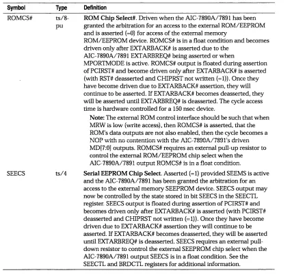
ROMCS# MI8 ts/8-pu
SEECS M17 ts/4
1 This signal requires an external pull-down resistor.
[image:26.617.107.491.123.368.2]Clock and Miscellaneous Pins
Table 2-5. Clock and Miscellaneous Pins
Signal Name Pin Number
va
Driver NoteseLKIN DI6 in
SCLKIN DI4 in
IDDAT N19 in-pu
EXTPAUSE# AI7 in-pu
PULLUPI MI in 2
PULLUP2 U3 in 2
1 This signal must be tied high or low if not used.
2 AIC-7890A only. This signal must be pulled up to PVCC with a 10 Kohm resistor.
Test Pins
Table 2-6. Test Pins
Signal Name Pin Number
TCK N1
TDI P2
TDO PI
TMS N2
TRST# M2
PDPUDIS# R20
TESTMODE# P19
1 This signal must be tied high or low if not used. 2 This signal must be tied low if not used.
110 Driver
in
in
ts/6 in
in
in
in
3 This signal must be tied to a known state. See Pin SiJ!I1a1 Description for more details. 4 This signal must be tied high during normal operati~n.
-Power and Ground Pins
Signal Name
AVCC1-AVCCO CVCC7 -CVCCO
~v1VCC6-~1VCCO
PVCC
SVCC8-SVCCO
AGND2-AGNDO GND
Table 2-7. Power and Ground Pins
Pin Number
B14, C14
B19, C3, B15, A18, P20, Y7, L4, G3 C17, D18, F18, G20, J20, L19, N18 D6, Dll, D15, F4, F17, K4, L17, R4, R17, U6, UIO, U15
D5, D7, C8, DIO, A12, K2, H3, E1, D2
D12, A13, B13
AI, D4, D8, D13, D17, H4, H17, 19, 110,111,112, K9, KIO, K11, K12, L9, L10,Ll1,L12,M9,M10,M11,M12, N4, N17, U4, U8, U13, U17
110 Driver
Notes
2
3
4
Notes
2
3
1 These BGA ball pads are connected to the power potential ring in the package.
2 A 10K + / -1% ohms resistor should be connected between pins C 13 and D 12. D 12 should not be connected to pins A13 and B13 on the board.
3 These BGA ball pads are connected to the die pad and the ground potential ring in the package.
AIC-7890AI1891 Data Book
2-6
Spare Pins
Signal Name
N/C
N/C
Table 2-8. Spare Pins
Pin Number
Y5, Yll, YI7, Y20, A20, PI8 M3, M4, N3, P3, P4, R3, T3, T4, V3, V4, U5, V5, V6, U7, V7, V8, U9, V9, VlO, Vll, U11, VI2, VI2, VI3, VI4, UI4, VI5, VI6, VI6, VI7, VI8, VI8, TI7, TI8, RI8, PI7, RI9
511683-00, Rev. B 8/17/98
Notes
Pin Signal Description
The logical state of a signal name that does not end in a
#symbol is asserted or active
when high and is deasserted or inactive when low. The logical state of a signal name that
ends in a
#symbol is asserted or active when low and is deasserted or inactive when high.
pel
Host Interface Pins
Symbol Type
ACK64# in
(AIC-7891 only)
AD[31:0] in-ts/6 (AIC-7890A)
Table 2-9. PCI Host interface Pins
Definition
PCI Acknowledge 64-bit Transfer Input is an active low signal that indicates the target is willing to transfer data using 64-bit. As a target, AIC-7891 doesn't transfer data in 64-bit; therefore, ACK64# is never driven by the AIC-7891.
PCI Address and data are multiplexed on the same PCI bus pin. During the flrst clock of a traIlsaction, AD[31:00] contain a physical byte address of
(32 bits) called low address 31:00 for Single Address Cycles (SAC). During subsequent clocks; AD[31:00] contaLn data of (32-bits) called low data 31:00; except for Dual Address Cycles (DAC) where both the first (low address 31 :00) and second (high address 63:32) clocks of a transaction contain address and the remaining clocks contain data (low data 31:00). The turn-around PCLK period for AD[31:00] is the idle cycle between transactions. A PCI read or write bus transaction consist of one Address phase (SAC) or two Address phases (DAC) followed by one or more Data phases. Each PCI Data phase may consist of one or more PCLK periods. Little-endian byte ordering is used. AD[07:00] define the least significant byte and AD[31:24] the most significant byte. All 32 AD[31:00] bits must be driven to stable values (excluding turn around PCLK periods) during every Address and Data phase, to enable even-parity checking. All AD[31:00] bits must be decoded for memory and I/O phases to allow for future address expansion. The use of AD[01:00] varies in the Address phase of the three different PCI address spaces:
• In the PCI Configuration address space, AD[01:00] identify the type of configuration space the access is intended for. A value of Oh identifies the configuration space as type 0; a value of 1h identifies it as type 1. Values of 2h and 3h are reserved. Type 0 configuration accesses are not propa-gated beyond the local PCI bus and must be claimed by a local device or terminated with master-abort. Type 1 configuration accesses are for tar-gets that do not reside on the local PCI bus. For type 0, AD[07:02] defme a 32-bit register address within the configuration address space. Thus, con-figuration address space defaults to Double Word (DWD) addressing aligned to the DWD boundary. Targets with multiple functions must con-tain a configuration space for each function. The value supplied on AD[lO:08] is used to point to each space. The AIC-7890A, as a single func-tion target supporting type 0 address space, accesses with a single config-uration space. As a target, the AIC-7890A uses positive address decoding over AD[1O:02], along with CBE[3:0]# (command is CRDC or CWRC), IDSEL, AD[01:00] = Oh and FRAME# to validate the configuration regis-ter address decode, then asserts DEVSEL# to claim the transaction. AD[1O:08] must be "000" to enable configuration access of the AIC-7890A. IDSEL is normally connected to an ADn signal in the range of AD[31:11] of the PCI bus.
AIC-7890AI7891 Data Book
Symbol
2-8
Table 2-9. PCI Host interface Pins (Continued)
Type Definition
• In the 10 address space, all 32 AD lines are used to provide for direct byte address decoding. The AIC-7890A as a target uses positive address decoding over BASEADRO register (stored value), AD[31:08] (for map-ping), CBE[3:0]# (for command), AD[07:00] (for register address) and FRAME# to validate the Device Space register 256 decodes. When the AIC-7890A as a target is enabled to allow access to its Device Space regis-ters from the PCI I/O address space, the use of AD[01:00] during the Address phase allows the AIC-7890A to validate the register address decode and claim the transaction (assert DEVSEL# = medium speed). TRDY# is deasserted for the first Data phase to allow the Data phase CBE value to become valid for byte steering to the internal8-bit register path for a three PCLK data transfer cycle for register write. For register read, TRDY# is deasserted for the required AD[31:00] turn-around cycle, plus an additional PCLK for H/W registers, plus one or more to enable inter-nal or exterinter-nal RAM data to become valid. Note, additiointer-nal PCLKs are required for some addresses, due to mode conditions. Many AIC-7890A registers are also accessed by the internal RISC PhaseEngine (sequencer) . • In the PCI memory address space, AD[01:00] are excluded from the
address decode and as such, the address defaults to Double Word (DWD) addressing aligned to the DWD boundary. The value AD[01:00] are used in the memory address space to indicate different Memory Address Transfer modes. A value of Oh indicates linear address increment mode, 1h is reserved (disconnect after fIrst data phase), 2h indicates Cache Line Wrap mode, and 3h is reserved. The AIC-7890A as a master or target only supports the linear address increment mode.
When the AIC-7890A as a target is enabled to allow access to its Device Space registers from the PCI memory address space, it will use positive address decoding over BASEADR1 register (stored value), AD[31:02], CBE[3:0]# (command) and FRAME# to obtain the DWD access decode and claim the transaction by asserting (DEVSEL# = medium speed). Then use the CBE[3:0]# (data) value to complete the Device Space register decode. TRDY# is deasserted for the fIrst Data phase to allow the Data phase CBE value to become valid for byte steering to the internal8-bit register path for a three PCLK data transfer cycle for register write. For register read TRDY # is de asserted for the required AD [31 :00] turn-around cycle, plus an additional PCLK for H/W registers, plus one or more to enable internal or external RAIvI data to become valid. Note, additional PCLKs are required for some addresses due to mode conditions. Many AIC-7890A registers are also accessed by the internal RISC PhaseEngine (sequencer)
When the AIC-7890A as a target is enabled to allow access to the expansion ROM address space through the AIC-7890A memory port to a local 8-bit ROM/EEPROM, the AIC-7890A will use positive address decoding over EXROMCTL register (stored value), AD[31:02], CBE[3:0]# (comma.'1d) and FRA}v1E# to obtain t..i.e DVVD access decode and claim the transaction by asserting (DEVSEL# = medium speed).
Symbol
Table 2-9. PCI Host interface Pins (Continued)
Type Definition
For Memory Read commands, the AIC-7890A will perform a burst of four read accesses of the external ROM/EEPROM to assemble a 32-bit value for the PCI Read command, regardless of the CBE[3:0]# value for the requested data. TRDY# is deasserted for additional PCLKs for the required AD[31:00] turn-around cycle and to enable the external ROM (150 nsec per cycle) data to become valid, and will be asserted when the 32-bits are valid.
For Memory Write commands, the AIC-7890A will write only the byte associated with the single asserted CBE[3:0]# to the external EEPROM. When no CBE[3:0]# are asserted, the write will be treated as an NOP. TRDY# will be deasserted for the external EEPROM write cycle access time (150 nsec) then will be asserted to terminate the PCI write access. Note: The ROM/EEPROM type and its connection to the AIC-7890A should be such that inadvertent writing when the type is ROM will not allow contention of the memory data bus. For both Read or Write commands, access w,ill be extended with TRDY# deasserted until EXTARBACK# becomes active. When a PCI burst is indicated it will be disconnected after the fIrst Data phase.
The use of AD[31:00] varies in the Data phase of transactions as follows when the AIC-7890A is a bus master or a bus target:
• Bus target Data phase transactions to the AIC-7890A's 8-bit Device Space registers will use the AD[31:00] byte indicated by a single asserted CBE# for all registers. Should more than one CBE# be asserted (indicates a non-supported data width), the AIC-7890A will indicate Target Abort. When more than one Data phase is indicated (burst operation), the AIC-7S90A will indicate Disconnect and only accept the fIrst Data phase. When no CBE bits are asserted, the AIC-7890A will not store the associated data for (write) and will supply all AD[31:00] bytes with Oh value for (read). • Bus target Data phase transactions to the AIC-7890A's confIguration
space supports up to (32-bit) data transfers on AD[31:00] with the valid data bytes indicated with the CBE[3:0]# value for (write), for (read) the AIC-7890A will always source all bytes of the addressed register. Reading reserved confIguration space register bytes/bits always return zero for the value. Data written to reserved confIguration space register bits or bytes is discarded No error indication is made for reading or writing to reserved registers. When more than one Data phase is indicated (burst operation), the AIC-7890A indicates Disconnect and only accepts the fIrst Data phase.
• The AIC-7890A as a master will always transfer leading offset data bytes, if they exist, to reach the next DWD boundary in the fIrst Data phase of a transaction, if the byte count is sufficient. Then four bytes will be trans-ferred at a time from DWD boundary to DWD boundary until the last Data phase, which will transfer any trailing offset bytes that may exist, to expire the byte count.
AIC·7890All891 Data Book
2-10
Symbol
AD[63:00] (AIC-7891 only)
Table 2-9. PCI Host interface Pins (Continued)
Type Definition
in-ts/6 PCI Address and Data are multiplexed on the same PCI bus pin. If REQ64# was not detected at the end of the reset(32-bit bus) or ACK64# was not asserted by the intended target, during the fIrst clock of a transaction AD[31:00] contain a physical byte address of (32-bits) called low address 31:00 for Single Address Cycles (SAC) command. During subsequent clocks, AD[31:00] contain data (32-bits) called low data 31:00, except for Dual Address Cycles (DAC) command where both the fIrst (low address 31:00) and second (high address 63:32) clocks of a transaction contain address and the remaining clocks contain data (low data 31:00). The turn-around PCLK period for AD[31:00] is the idle cycle between transactions. A PCI read or write bus transaction consist of one Address phase (SAC) or two Address phases (DAC) followed by one or more Data phases. Each PCI Data phase may consist of one or more PCLK periods. Little-endian byte ordering is used. AD[07:00] defIne the least signifIcant byte and AD[31:24] the most signifIcant byte. All 32 AD[31:00] bits must be driven to stable values (excluding turn around PCLK periods) during every Address and Data phase, to enable even-parity checking. All AD[31:00] bits must be decoded for memory and 110 phases to allow for future address expansion.
If REQ64# was detected at the end of the reset(64-bit bus) and ACK64# was asserted by the intended target, during the first clock of a Single Address Cycles (SAC) command, AD[31:00] contain a physical byte address of (32-bits) called low address 31:00. During subsequent clocks, AD[63:00] contain data (64-bits) called low data 63:00. During the fIrst clock of a transaction of a Dual Address Cycles (DAC) command, AD{63:00] contain a physical byte address (64-bits) called address 63:00, and during second clocks of a transaction, both AD[31:00] and AD[63:32] contain upper 32-bit address. During subsequent clocks, AD[63:00] contain data (64-bits) called data 63:00 The use of AD[01:00] varies in the Address phase of the three different PCI address spaces:
• In the PCI ConfIguration address space, AD[01:00] are used to identify the type of confIguration space the access is intended for. AD[Ol:OO] are a value of Oh to identify the confIguration space as type 0 and a value of Ih for type 1, with values of 2h and 3h reserved. Type 0 confIguration accesses are not propagated beyond the local PCI bus and must be claimed by a local device or terminated with master-abort. Type 1 confIg-uration accesses are for targets that do not reside on the local PCI bus. For type 0, AD[07:02] defIne a 32-bit register address within the confIguration address space. Thus, confIguration address space defaults to Double Word (DWD) addressing aligned to the DWD boundary. Targets with multiple functions must contain a confIguration space for each function. The value supplied on AD[1O:08] is used to point to each space. The AIC-7891. as a single function target supporting type 0 address space, accesses with a single configuration space. The AIC-7891 as a target, uses positive address decoding over AD[07:02] along with CBE[3:0]# (command is CRDC or CVvRC), IDSEL, AD[Oi:OOj
=
Oh, AD[1O:08]=
OOXb and FRAME# to validate the confIguration register address decode, then asserts DEVSEL# to claim the transaction.Symbol
Table 2-9. PCI Host interface Pins (Continued)
Type Definition
• In the 10 address space, all 32 AD lines are used to provide for direct byte address decoding. The AIC-7891 as a target uses positive address decod-ing over BASEADRO register (stored value), AD[31:08] (for mappdecod-ing), CBE[3:0]# (for command), AD[07:00] (for register address) and FRAME# to validate the Device Space register 256 decodes .
• When the AIC-7891 as a target is enabled to allow access to its Device Space registers from the PCI 10 address space, the use of AD[01:00] dur-ing the Address phase allows the AIC-7891 to validate the register address decode and claim the transaction (assert DEVSEL# = medium speed). TRDY# is deasserted for the fIrst Data phase to allow the Data phase CBE value to become valid for byte steering to the internal8-bit register path for a three PCLK data transfer cycle for register write. For register read, TRDY# is deasserted for the required AD[31:00] turn-around cycle, plus an additional PCLK for H/W registers, plus one or more to enable internal or external RAi\r1 data to become valid. Note: Additional PCLKs are required for some addresses, due to mode conditions.
ii In the PCI memory address space, AD[01:00] are excluded from the
address decode and as such, the address defaults to Double Word (DWD) addreSSing aligned to the DWn boundary. The value AD[Ol:00] are used in the memory address space to indicate different Memory Address Transfer modes. A value of Oh indicates linear address increment mode, a value of Ih indicates Address Cache Line Toggle mode, and the values of 2h and 3h are reserved. The AIC-7891 as a master or target only supports the linear address increment mode,
When the AIC-7891 as a target is enabled to allow access to its Device Space registers from the PCI memory address space, it will use positive address decoding over BASEADRI register (stored value), AD[31:02], CBE[3:0]# (command) and FRAME# to obtain the DWD access decode and claim the transaction by asserting (DEVSEL# = medium speed). Then use the CBE[3:0]# (data) value to complete the Device Space register decode. TRDY# is deasserted for the fIrst Data phase to allow the Data phase CBE value to become valid for byte steering to the internal8-bit register path for a three PCLK data transfer cycle for register write. For register read TRDY# is deasserted for the required AD[31:00] turn-around cycle, plus an additional PCLK for H/W registers, plus one or more to enable internal or external RAM data to become valid. Note, additional PCLKs are required for some addresses due to mode conditions.
When the AIC-7891 as a target is enabled to allow access to the expansion ROM address space through the AIC-7891 memory port to a local8-bit ROM/EEPROM, the AIC-7891 will use positive address decoding over EXROMCTL register (stored value) in ConfIguration space, AD[31:02], CBE[3:0]# (command) and FRAME# to obtain the DWD access decode and claim the transaction by asserting (DEVSEL# = medium speed).
AIC-7890An891 Data Book
Symbol
2-12
Table 2-9. PCI Host interface Pins (Continued)
Type Definition
For Memory Read commands, the AIC-7891 will perform a burst of four read accesses of the external ROM/EEPROM to assemble a 32-bit value for the PCI Read command, regardless of the CBE[3:0]# value for the requested data. TRDY# is de asserted for additional PCLKs for the required AD[31:00] turn-around cycle and to enable the external ROM (150 nsec per cycle) data to become valid, and will be asserted when the 32-bits are valid.
For Memory Write commands, the AIC-7891 will write only the byte associated with the single asserted CBE[3:0]# to the external EEPROM. When no CBE[3:0]# are asserted, the write will be treated as an NOP. TRDY# will be deasserted for the external EEPROM write cycle access time (150 nsec) then will be asserted to terminate the PCI write access. Note: The ROM/EEPROM type and its connection to the AIC-7891 should be such that inadvertent writing when the type is ROM will not allow contention of the memory data bus. For both Read or Write commands, access will be extended with TRDY# deasserted until EXT ARBACK# becomes active. When a PCI burst is indicated it will be disconnected after the fIrst Data phase.
The use of AD[63:00] varies in the Data phase of transactions as follows when the AIC-7891 is a bus master or a bus target:
• Bus target Data phase transactions to the AIC-7891 's 8-bit Device Space registers will use the AD[31:00] byte indicated by a single asserted CBE[3:0]# for all registers. Should more than one CBE[3:0]# be asserted (indicates a nonsupported data width), the AIC-7891 will indicate Target Abort. When more than one Data phase is indicated (burst operation), the AIC-7891 will indicate Disconnect and only accept the fIrst Data phase (except for SCB double word write, where bursting is allowed, with linear burst order only). When no CBE bits are asserted, the AIC-7891 will not store the associated data for (write) and will supply all AD[31:00] bytes with Oh value for (read).
• Bus target Data phase transactions to the AIC-7891 's configuration space supports up to (32-bit) data transfers on AD[31:00] with the valid data bytes indicated with the CBE[3:0]# value for (write), for (read) the AIC-7891 will always source all bytes of the addressed register. Reading reserved confIguration space register bytes/bits always return zero for the value. Data written to reserved confIguration space register bits or bytes is discarded No error indication is made for reading or writing to reserved registers. When more than one Data phase is indicated (burst operation), the AIC-7891 will indicate Disconnect and only accept the first Data phase.
• The AIC-7891 as a master will always transfer leading offset data bytes, if they exist, to reach the next DWD boundary for 32-bit bus or QWD boundary for the 64-bit bus in the fIrst Data phase of a transaction, pro-viding the byte count is sufficient. Then multiple of 4 or 8 bytes are trans-ferred depending on the bus width until the last Data phase, which will transfer any trailing offset bytes that may exist, to expire the byte count.
Symbol
CBE[3:0]# (AIC-7890A)
CBE[7:0]:Jt
(AIC-7891 only)
Table 2-9. PCI Host interface Pins (Continued)
Type Definition
in-ts/6 Bus Command and Byte Enables are multiplexed on the same PCI pins. During the Address phase of a transaction, CBE[3:0]# contain a Bus command that dermes the function to be perfonned during the transaction. CBE[3:0]# command encodings are viewed on the bus where a 1 indicates a high voltage and 0 is a low voltage. During the Data phase of a transaction, CBE[3:0]# define which data bytes of AD[31:00] contain valid data. CBEO# applies to AD[07:00] and CBE3# to AD[31:24]. The AlC-7890A asserts CBE[3:0]# when in master mode to indicate the location of the first byte in a 32-bit boundary space and to match the data width being transferred. CBE[3:0]# are asserted (=0) by the system board or a bus master to access the AlC-7890A as a bus slave. No more than one CBE# may be asserted at a time for transactions to the AIC-7890A's 8-bit Device registers without causing a Target Abort reply.
Note: Data phases that do not have at least one asserted CBEn# do not transfer data, however all data bytes must be stable so that pariry may be developed, and appear as NOPs on the bus.
in-ts/6 Bus Command and Byte Enables are multiplexed on the same PCI pins. During the Address phaSe of a transaction, CBE[3:0]# contain a Bus command that defines the function to be perfonned during the transaction. CBE[3:0]# command encodings are viewed on the bus where a 1 indicates a high voltage and 0 is a low voltage. During an address phase of a DAC command with REQ64# asserted, the actual bus command is transferred on CBE[7:4]#; otherwise, these signals are reserved and indetenninate. During the Data phase of a transaction, CBE[3:0]# derme which data bytes of AD[31:00] contain valid data. CBEO# applies to AD[07:00] and CBE3# to AD[31:24]. When both REQ64# and ACK64# are asserted, CBE[7:4] define which data bytes of AD[63:32] contain valid data. CBE4# applies to AD[39:32] and CBE7# to AD[63:56].
When in the master mode, if REQ64# was not detected at the end of the reset by the AlC-7891 or the AlC-7891 only intends to access the lower 32-bit space (AD[63:32] are zero), the AIC-7891 asserts CBE[3:0]# to indicate the location of the first byte in a 32-bit boundary space and to match the data width being transferred. If REQ64# was detected at the end of the reset by the AlC-7891 and the AlC-7891 intends to access the upper 32-bit space (AD[63:32] are not zero), the AIC-7891 asserts CBE[7:0]# to indicate the location of the first byte in a 64-bit boundary space and to match the data width being transferred.
CBE[3:0]# are asserted (=0) by the system board or a bus master to access the AlC-7891 as a bus slave. No more than one CBE[3:0]# may be asserted at a time for transactions to the AlC-7891's 8-bit Device registers without causing a Target Abort reply. Note that AlC-7891 supports 32-bit only as a PCI target.
Note: Data phases that do not have at least one asserted CBEn# do not transfer data, however all data bytes must be stable so that parity may be developed, and appear as NOPs on the bus.
AIC·7890AI7891 Data Book
Symbol
DEVSEL#
FRAME#
2-14
Table 2-9. PCI Host interface Pins (Continued)
Type Definition
in-sts/6 Device Select#". When asserted, indicates the driving device has decoded its address as the selected target of the current bus transaction. DEVSEL# once asserted cannot be deasserted until FRAME# is sampled deasserted, except for the target -abort case. Also DEVSEL# must be asserted for one or more PCLKs before a target-abort condition may be signaled. The
AIC-7890A/7891 as a slave asserts DEVSEL# with medium speed timing when responding as a result of a valid and supported command directed to the AIC-7890A/7891's Configuration register space, and when enabled, to the Device register space, or to the external ROM. The AIC-7890A/7891 as a master, samples DEVSEL#" when initiating a transaction to a selected target to determine if the target is capable of proceeding with the current
transaction. In the case when DEVSEL# is not asserted by the selected target for six PCLKs (SAC) or seven PCLKs (DAC) after FRAME# is asserted, the
AIC-7890A/7891 will perform a master-abort (on PCLK seven (SAC) or eight (DAC) deassert FRAME# on the next PCLK (if still asserted) and on the next PCLK deassert IRDY#). Alternately where FRAME# was deasserted after one PCLK (indicates only one Data phase in the transaction), the AIC-7890A/7891 will perform a master-abort (on PCLK seven (SAC) or eight (DAC) deassert IRDY#). The AIC-7890A/7891 will not retry transactions that resulted in a master-abort (no response from target) and will generate an interrupt to the driver with RMA status active set in the respective configuration space register. Intervention is required for the AIC-7890A/7891 to continue with bus master transactions after a master abort is generated. The turn-around PCLK period for DEVSEL# is the Address phase of a transaction. The AIC-7890A/7891 as a master never asserts DEVSEL#".
in-sts/6 Frame#". Asserted by the current master to indicate the duration of a bus transaction. The assertion of FRAME# identifies an Address phase of a transaction. The deassertion of FRAME# identifies the fmal data phase of the transaction (FRAME#" cannot be deasserted while IRDY# is deasserted for the fmal data phase). An idle cycle (PCI bus free) occurs when both FRAME# and IRDY# are deasserted. The turn-around PCLK period for FRAME# is the idle cycle between transactions. See DEVSEL# for the AIC-7890A/7891 Master-Abort conditions. The AIC-7890A/7891 as a target never asserts FRAME#.
The AIC-7890A/7891 asserts FRAME# with the same PCLK that asserts an address value on AD[31:00J for SAC or DAC. When the transaction is a DAC, FRAME# remains asserted for the second PCLK Address phase and for all Data phases that follow, until the last data phase where FRAME# will be deasserted.
Symbol
GNT#
IDSEL
IRDY#
Table 2-9. PCI Host interface Pins (Continued)
Type Definition
in Grant#. Asserted indicates to a master that a bus transaction may be performed. This is a point-to-point signal with every master having its own GNT# signal. Only one GNT# may be asserted by the PCI System Board Central Resource Arbitrator at a time. The Arbitrator may deassert GNT# at any time (one PCLK period minimum assertion) and may also assert GNT# when the master is not asserting PREQ# (park the bus) to require the master to drive bus signals AD[31:00] (AD[63:00] for 64-bitbus), CBE[3:0]#
(CBE[7:0]# for 64-bit bus) and PAR delayed by one PCLK within eight PCLK (recommended value is by two to three PCLKs) to prevent bus float conditions. In the case where GNT# is deasserted and FRAME# is asserted on the same PCLK, the bus transaction is valid and will continue. One GNT# can be deasserted coincident with another GNT# being asserted if the bus is not idle. Otherwise a one PCLK delay is required between the de assertion of one GNT# and the assertion of the next GNT#. The newly granted master may not start a transaction until a.T} IDLE cycle (FRAr.v1E# and IRDY# deasserted) is sampled. GNT# is held in a tri-stated condition while PCIRST# is asserted. The AIC-7890A!7891 extends an asserted PCIRST# internally and thus will not recognize GNT# in any state until after the extension expires. Except for the PCIRST# condition, the
AIC-7890A/7891 will drive AD[31:00] (AD[63:00] for 64-bit bus) and CBE[3:0]# (CBE[7:0]# for 64-bit bus) on the first PCLK, GNT# is sampled asserted with the PCI bus idle, then PAR one PCLK later.
in Initialization Device Select. Used in lieu of the upper 24 ADn address signals and is valid only during configuration read and write transactions and is validated with FRAME# assertion, valid AD[10:8], and CBEn# values. IDSEL is a point-to-point signal with each agent having its own IDSEL. PCI convention is to connect a different AD[31:11] line to IDSEL input of each device on the bus.
in-sts/6 Initiator Ready#. Asserted to indicate the current master's ability to complete the current Data phase of a transaction. During a write, IRDY# indicates that the master is asserting valid data on AD[31:00] (AD[63:00] in the 64-bit transfer). During a read, it indicates the master is prepared to accept data on AD[31:00] (AD[63:00] in the 64-bit transfer). It is used in conjunction with TRDY#. Wait cycles are inserted until both IRDY# and TRDY# are asserted together. A Data phase is completed on any PCLK when IRDY# and TRDY# are both sampled asserted. An idle cycle (PCI bus free) occurs when both FRAME# and IRDY# are deasserted. The turn-around PCLK period for IRDY# is the Address phase of a transaction. The AIC-7890A/7891 as a master asserts IRDY# with the same PCLK that starts a Data phase on AD[31:00] (AD[63:00] in the 64-bit transfer).
AIC-7890An891 Data Book
2-16
Symbol
PAR
PAR64 (AIC-7891 only)
PCLK
Table 2-9. PCI Host interface Pins (Continued)
Type Definition
in-ts/6 Parity. The even-parity bit that protects both AD[31:00] and C/BE[3:0]# signals. PAR is generated by the agent that is sourcing the 32-bit address of the transaction and/or the data of the transaction and includes the CBE[3:0] values even if not sourcing them. The state of PAR is valid for the value on AD[31:00] and CBE[3:0] during the previous PCLK period for address and for the PCLK that transferred data, excluding PAR turn-around PCLK periods which occur in the PCLK following the turn-around PCLK period of AD[31:00]. The agent detecting parity errors will set the DPE bit in the Configuration Status register without regard for the state of PERRESPEN bit. The AIC-7890A/7891 as a target indicates SERRfor address parity error detection when both PERRESPEN and SERRESPEN are active. The AIC-7890A/7891 as a target will assert PERR for data parity errors when PERRESPEN is active.
in-ts/6 Parity. The even-parity bit that protects both AD[63:32] and C/BE[7:4]# signals. PAR64 is generated by the agent that is sourcing the upper 32-bit PCI address of the transaction and/or the upper 32-bit data of the
transaction and includes the CBE[7:4] values even if not sourcing them. The state ofPAR64 is valid for the value on AD[63:32] and CBE[7:4] during the previous PCLK period for address and for the PCLK that transferred data, excluding PAR64 turn-around PCLK periods which occur in the PCLK following the turn-around PCLK period of AD[63:32]. The agent detecting parity errors will set the DPE bit in the Configuration Status register without regard for the state of PERRESPEN bit. The AIC-7891 as a target indicates SERR for address parity error detection when both PERRESPEN and SERRESPEN are active. The AIC-7891 as a target will assert PERR for data parity errors when PERRESPEN is active.
in PCI Bus Clock Input. Provides timing for all transactions on the PCI bus. All other PCI signals are sampled on the rising edge of PCLK, and all parameters are defined with respect to this edge. PCLK is a controlled skew, point-to-point signal to each agent and is only driven by the PCI System Board Central Resource. The PCLK signal for the AIC-7890A/7891 is a maximum rate of 33.3 MHz. When POWRDN is active, the
AIC-7890A/7891 restricts the use of PCLK to only Configuration address space and the AIC-7890A/7891 Device registers which are accessible only from the PCI bus (not from the internal sequencer). PCLK signal used by other logic is maintained in the active state (=1) when POWRDN is active. Note, all internal logic is static allowing the PCLK and the CLKIN signals to be stopped externally if desired when no active SCSI commands are in process for maximum power down mode.
Symbol
PERR#
PREQ#
REQ64# (AIC-7891 only)
PCIRST#
Table 2-9. PCI Host interface Pins (Continued)
Type Definition
in-sts/6 Parity Error#. May be asserted (pulsed for one PCLK period for each detected error, provided that the Parity Error Response bit, PERRESPEN, is active in the Configuration Command register) only by the agent receiving the data. Also, a target cannot assert PERR# until it has claimed the access by asserting DEVSEL# and completing the data transfer. The turn-around PCLK for PERR# is the third PCLK period after the last address PAR and/ or P AR64 period of an agent. PERR# is asserted for detected errors two PCLK periods after the data that contained the error as per the following sequence:
1 From PCLK N that transfers the data (both TRDY# and IRDY# are asserted) that data parity is to be generated for.
2 From PCLK N + 1 PAR is asserted for the data asserted in PCLK N. 3 From PCLK N+2 assert PERR# when an even-parity error was
indicated on the PCLK N+ 1 sample of data.
4 From PCLK (N+2)+1 de assert PERR# and when the last PERR# cycle wait for one more PCLK period before floating PERR#.
The AIC-7890A/7891 asserts PERR# only for detected data parity errors for received data when PERRESPEN is active but always sets DPE bit active in the Configuration Status register. The DPE bit is set in the Configuration status register if the parity error was detected for either the data of command channel.
ts/6 PCI Request#. When asserted, indicates to the PCI System Board Arbitrator that a master desires use of the bus. This is a point-to-point signal with every master having its own PREQ#. Arbitration for the PCI bus is performed either when the bus is idle or in parallel with the transaction in process. When only a single Data phase is to be performed, PREQ# should be deasserted with the same PCLK that asserts FRAME#. When a
transaction is terminated by a target, the master must deassert its PREQ# for a minimum of two PCLK periods (one period must include the bus idle period). This allows another agent to use the bus while the previous target (that requested the STOP) prepares to continue.
Note: This is not required where the master deasserted FRAME# indicating the last Data phase of a transaction is in process. In this case, provided GNT# is still asserted, the master could start another
transaction without de asserting PREQ#.
PREQ# is asserted by the AIC-7890A/7891 to become a bus master provided that the MASTEREN bit is active in the PCI configuration Command register.
in-ts/6 Request 64#. It is used by AIC-7891 to determine if it is connected to a 64-bit data path when PCIRST# is asserted. During the normal operation, AIC-7891 uses this signal to indicate to the target that AIC-AIC-7891 desires to transfer data using 64 bits.
in PCI Reset#. When asserted forces agents to a known initialization state. PCIRST# may be asynchronous to PCLK when asserted or deasserted. Deassertion is guaranteed to be a clean, bounce-free edge.
• All tri-state and sustained tri-state are forced to a high impedance state. • All 0/ d type signals are forced to float.
• All agent internal registers (Device and Configuration) are forced to spec-ified states.
• All internal RAM data values should be considered indeterminate.
AIC-7890AIl891 Data Book
Symbol
SERR#
STOP#
2-18
Table 2-9. PCI Host interface Pins (Continued)
Type Definition
in-od/6 System Errorl. May be asserted by a PCI agent that detects an address parity error (provided that PERRESPEN and SERRESPEN are active) during the Address phase of a transaction or for data parity errors on special cycles and for any other system error where the result will be a catastrophic error. The transaction master is solely re