Design, Modelling & Simulation Analysis of
Electromagnetic Pulse (EMP) Coupling to
Microstrip
Priti Mandal1, B.Venkata Ramana2, Dr. PVY Jayasree3
1
M.Tech (RFME) Student, GITAM (Deemed to be University), Visakhapatnam, A.P, India 2
Scientist-C, SAMEER-CE3, Visakhapatnam, A.P India 3
Professor (HOD) GITAM (Deemed to be University) Visakhapatnam, A.P, India
Abstract: This paper is to analyze the EMP coupling to microstrip using 3D EM Modeling and Simulation Analysis. Developed bounded wave transmission line structure as per MIL-STD 461, RS105 EMP requirement in terms of peak electric field of 50KV/m with rise time-2.3ns and pulse width-25ns. Microstrip is modeled. EMP Coupling to cables was carried out by placing the microstrip under generated EMP field in terms of induced voltage and currents due to EMP fields.
Keywords: Electromagnetic pulse (EMP), Bounded wave Transmission line, microstrip, EMP field, Coupling.
I. INTRODUCTION
A. Electromagnetic Pulse
An electromagnetic pulse is a short burst of electromagnetic energy. EMP arises from two principal sources, the first of which is the gamma rays emitted by the nuclear detonation. The second significant type of EMP from high altitude bursts is a low frequency, low amplitude field caused by explosion plasma motion in the upper atmosphere. This environment is commonly referred to as magneto-hydrodynamic EMP or MHD EMP. EMP have devastating effect on the unprotected electronics systems.
Gamma rays represent about 1/1000th of the total bomb energy and are emitted within ten billionths of a second. The amount of gamma emitted by a one- megaton detonation is about 4 X 10¹² Joules. The gamma rays, by a process known as the “Compton Effect,” strip electrons from air molecules to create a large-scale electron current in the upper atmosphere. This electron current is deflected by the earth’s magnetic field and thereby radiates an intense electromagnetic pulse (EMP) over extensive portions of the earth’s surface. Effects extend to ground areas within the line-of-sight of the burst as shown in fig.
Fig. 1 Mechanism of gamma-induced EMP from a high-altitude burst
B. Microstrip
Microstrip is used for transmission of microwave-frequency signals. Substrate separates the conductor and the ground plane. From microstrip, Microwave components can be formed such as antennas, power dividers, couplers, filters etc. with the entire device existing as the pattern of metallization on the substrate. As compared to other traditional waveguide technology Microstrip is less expensive, lighter weight and more compact. Microstrip lines are used in high-speed digital PCB designs, where signals need to be routed from one part of the assembly to another with minimal distortion, and avoiding high cross-talk and radiation.
Fig.2 Microstrip
II. BOUNDEDWAVETRANSMISSIONLINESTRUCTURE
Transverse electromagnetic (TEM) cell type of triangular transmission line with a matching termination resister bank will be best structure for generating EMP pulse with minimum distortions. Generally radiating lines will be made with multiple metal wires terminated with distributed load resistors. Bottom ground plane resistors will of metallic mesh for simulation the TEM cell type structure.
Fig.3 Radiation Line (Triangular)
In the triangular radiation line, the pulse produced by the HV generator is transformed into a TEM electromagnetic field travelling in the direction of the load. Because there is no discontinuity along the line, no other electromagnetic modes than TEM are exited. Some reflections are induced due to the construction of load.
In the parallel plate, between the slope (triangular part) and the flat part the wave is travelling up to the transition placed. In this region other modes than TEM are produced that induce reflections and field distortions. At the end of the flat part process is repeated and finally the reflections are influenced by terminated load.
A. Modeling Of Bounded Wave Transmission Line Structure
Modelled bounded wave transmission line structure with matched terminated resistors for generating standardized EMP field. As an input Double Exponential voltage pulse is given and measured at equipment zone area.
Fig.4 CAD model of Bounded Wave Transmission Line structure
We placed probes at the place of EUT to measure the E.F at each probe. As shown in figure below-
Fig.5 CAD model of Bounded Wave Transmission Line structure with probes
Fig.6 Boundary condition applied in all directions
Fig.7 Electric field obtained at different probes
III.SIMULATION A. Microstrip Inside Bounded Wave Transmission Line Structure
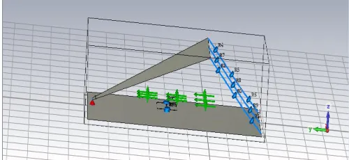
In this we have placed microstrip inside Bounded Wave Antenna Structure at EUT and observe the coupling effect. There are four resistors- source resistor, near end resistor, far end resistor and load resistors ,Rs, Rne, Rfe, Rl 50 ohm each respectively as shown in figure. As an input Double Exponential voltage pulse is given and measured at equipment zone area.
[image:4.612.175.448.145.274.2]
Fig 8 CAD model of Microstrip placed inside Bounded Wave Transmission Line Structure
Fig .9 CAD model of Microstrip placed inside Bounded Wave Antenna Structure with probes
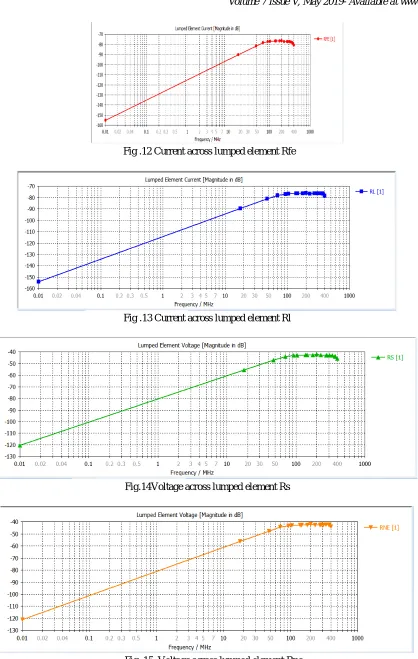
Fig .10 Current across lumped element Rs
[image:4.612.199.449.303.418.2]
[image:5.612.99.517.55.714.2]
Fig .12 Current across lumped element Rfe
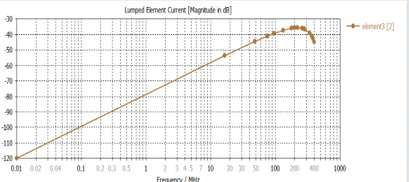
Fig .13 Current across lumped element Rl
Fig.14Voltage across lumped element Rs
Fig .16 Voltage across lumped element Rfe
Fig .17 Voltage across lumped element Rl
B. Microstrip With Source Inside Bounded Wave Transmission Line Structure
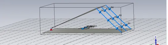
In this we have placed microstrip inside Bounded Wave Antenna Structure at EUT and observe the coupling effect. There are 2 ports. Port 1 is discrete port which is connected between the ground plate and upper plate and port 2 is a waveguide port which is connected to one of the strip and the ground of the microstrip. Rest three are connected with resistors- near end resistor, far end resistor and load resistors , Rne, Rfe, Rl 50 ohm each respectively as shown in figure. As an input Double Exponential voltage pulse is given and measured at equipment zone area.
[image:6.612.173.455.525.602.2]
Fig 18 CAD model of Microstrip placed inside Bounded Wave Transmission Line Structure
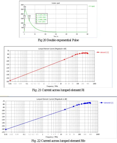
Fig 20 Double exponential Pulse
[image:7.612.119.495.75.536.2]Fig .21 Current across lumped element Rl
[image:7.612.125.488.551.708.2]Fig .22 Current across lumped element Rfe
Fig.24 Voltage across lumped element Rl
Fig.25 Voltage across lumped element Rfe
Fig.26 Voltage across lumped element Rne
Fig .28 Current across lumped element Rfe due to port2
Fig.29Current across lumped element Rne due to port2
Fig.30 Voltage across lumped element Rl due to port2
[image:9.612.136.488.375.712.2]Fig.32 Voltage across lumped element Rne due to port2
C. Microstrip
In this we have modelled microstrip. Microstrip consists of three layers- conductor, dielectric layer, and ground. There are two strips. In one strip one side is connected to port 2 (waveguide port ) and other side with load resistor and other strip both the side is
connected with both the resistors near end resistor and far end resistors with all the resistor 50 ohms each.
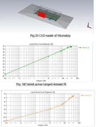
Fig.33 CAD model of Microstrip
[image:10.612.170.480.293.406.2]
Fig .34Current across lumped element Rl
[image:10.612.170.487.297.716.2]
Fig .36Current across lumped element Rne
[image:11.612.163.502.187.720.2]
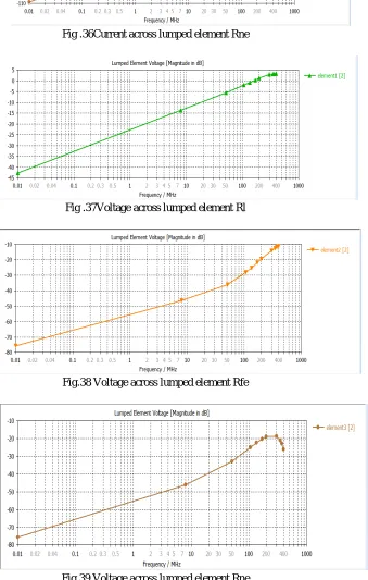
Fig .37Voltage across lumped element Rl
[image:11.612.168.493.242.368.2]
Fig.38 Voltage across lumped element Rfe
[image:11.612.167.505.554.707.2]
IV.RESULT
Table1. Comparison of current and voltage (in dB) at 100MHz RESISTORS MICROSTRIP
(with source) (at 100MHz)
Voltage Current
(in dB) (in dB)
MICROSTRIP PLACED INSIDE THE BWT
(at 100MHz)
Voltage (in dB) Current(in dB)
MICROSTRIP WITH SOURCE PLACED INSIDE THE BWT (at 100 MHz)
Due to port 1 Due to port 2
Voltage Current Voltage Current (in dB) (in dB) (in dB) (in dB)
Rs - - -42 -78 - - - -
R ne -25 -37 -42 -78 -50 -80 -5 -40
R fe -30 -67 -42 -78
-50 -80 -15 -45
R l -2.5 -37 -42 -78
-50 -80 16.7 -17.25
V. CONCLUSION
Bounded Wave Transmission Line Structure is modeled. The electric field at different positions (h/3, w/2) within EUT volume is measured using E-Field probe. EMP Coupling to microstrip was carried out by placing the microstrip under generated EMP field in terms of induced voltage and currents due to EMP fields. The microstrip coupling was analyzed with both EMP and without EMP as well as with and without source. Thus from the analysis it can be said that microstrip under the EMP will have more coupling as compared to the microstrip without EMP with source connected to one of the strip of the microstrip. Whereas coupling is less in the microstrip in which both the strips are connected to the four resistors.
REFERENCES [1] https://www.cst.com
[2] https://www.montena.com
[3] Referred to SAMEER, Vizag website-ce3.sameer.gov.in. [4] https://whatis.techtarget.com/definition/electromagnetic-pulse-EMP
[5] https://www.electronics-notes.com/...electromagnetic-interference.../what-is-emi-basics
[6] https://www.iosrjen.org/Papers/vol2_issue6%20(part-1)/L02613401344.pdf -Bounded Wave Transmission Antenna Structure. [7] Sandeep Kumar et al. International Journal of Recent Research Aspects ISSN: 2349-7688, Vol. 2, Issue 4, December 2015, pp. 10-14. [8] Interaction notes of EMP.