Abstract—Jitter is a matter of great concern for high-speed digital designers because of its ability to degrade the overall system performance. Designing a low-jitter and wide-band phase locked loop (PLL) system is of practical importance because of its application in high speed digital systems. This paper presents experimental results of a low-jitter wide-band dual cascaded PLL system using a single crystal oscillator. The first PLL employs a voltage-controlled crystal oscillator (VCXO) to eliminate the input jitter whereas the second PLL provides wide bandwidth. Field Programmable Gate Array (FPGA) is used to generate a jittered clock source which is then passed through the proposed system to achieve wide-band and low-jitter signal. Experimental results are presented to validate the proposed technique for different carrier frequencies.
Index Terms—FPGA, Hardware, Low Jitter, Phase Locked Loop (PLL), Wide-band system.
I. INTRODUCTION
Phase locked loop (PLL) is a negative feedback loop basically used to synchronize an output signal with a reference or input signal in phase as well as frequency [1]. A basic PLL consists of three main blocks, namely, the phase detector, the loop filter and the voltage controlled oscillator (VCO). PLL is designed to simplify different tasks such as clock recovery, data retiming, frequency translation and clock smoothing applications. The output signal from the PLL suffers from an associated jitter [2], [3], [4], [5] especially at high bit rate resulting in elevated bit error rate (BER) at the receiver side which may cause serious malfunctioning of the overall system if this error exceeds a certain threshold level.
Jitter is defined as the misalignment of edges in a sequence of data bits from their ideal positions and it can cause data errors. Three main types of jitter are cycle-to-cycle jitter [6], period jitter [7] and long-term jitter [8]. As the recovered signal is always jittered it is important to pass the signal through a special circuit to achieve a jitter free or low-jitter signal.
The objective of this paper is to experimentally investigate a low-jitter and wide-band system using two PLLs in cascade configuration. Behavioral modeling and simulation of the proposed system has already been dealt with in a previous paper [9]. Two PLLs as compared to single PLL are capable of operating over a wide frequency range meeting all the Manuscript received July 15, 2010. This work was financially supported by Research Center in the College of Engineering, King Saud University.
Authors are with the Department of Electrical Engineering, College of Engineering, King Saud University, Riyadh 11421, Saudi Arabia (emails: [email protected], [email protected]).
requirements of the individual standards in telephone carrier system.
The remainder of this paper is organized as follows. Section II presents a brief review of jitter reduction techniques. The details of dual cascaded PLL model is discussed briefly in section III. Section IV presents the experimental setup of the proposed system. Experimental results are further discussed in section V. Finally, conclusions are presented in section VI.
II. JITTER REDUCTION TECHNIQUES
In order to reduce the jitter, it is important to identify the root cause. Many jitter reduction techniques have been reported in the open literature. One of these techniques is to change the filter design to narrow down the PLL bandwidth and to make the phase noise at the VCO input as low as possible [10], [11]. Another technique is to reduce the power supply noise [12], [13]. Heydari et al. proposed a mathematical model for calculating the power supply noise inducing timing jitter in PLLs. This is done by eliminating ground bounce, using additional filter to minimize the effect of the sudden changes of the supply voltage and by having a good grounding to discharge the unexpected charges to ground [13].
A technique proposed for high frequency is by using dual phase frequency detector [14]. This design uses two phase detectors, the first phase detector is a multiplier and the second one is a phase and frequency detector. In [15], a modified low power consumption charge pump is used as phase frequency detector which proved useful in improving the jitter characteristics of a PLL by blocking the control voltage leakages.
Finally, using a PLL with voltage controlled crystal oscillator (VCXO) helped in generating a stable, low-jitter clock in the recovered signal [16]. A drawback of such technique is that one has to use a VCXO with the same frequency of the input jittered clock. This means that each carrier system needs to use a VCXO working at the same clock frequency. For example, for E1 telephone carrier
system, VCXO has to provide exactly 2.048 MHz signal.
III. DUAL CASCADED PLL SYSTEM
The two important solutions usually used for reducing jitter are those given in [11], [16]. Both these techniques work properly and were successful in reducing the jitter appreciably especially the second one is more effective. Both these techniques may be used for only one bit rate or clock
Experimental Results for Low-Jitter Wide-Band
Dual Cascaded Phase Locked Loop System
frequency.
[image:2.595.313.544.44.411.2]For example, in the second technique, a separate VCXO is needed for each bit rate. However, in this paper, we present dual cascaded PLLs as shown in figure 1. The recovered clock from the first loop is jitter bounded due to the effect of the VCXO. The second loop is a wide frequency band (wide lock-in range) to cover several standard data rates.
Figure 1: Dual cascaded PLL system
Under steady state operation and while the two loops are in locking conditions, we can deduce the following relationship: in out
f
M
M
N
N
f
2 1 2 1
(1)The above relationship shows that the output frequency fout may be programmed by selecting (N1, N2, M1 and M2) to be
equal to fin, independent of VCXO frequency when N1N2 =
M1M2. It means that we can generate several clock
[image:2.595.69.285.147.272.2]frequencies using single VCXO. The system presented in figure 1 is tested experimentally. The details of the experimental setup and the results obtained are presented in the following sections.
IV. EXPERIMENTAL SETUP
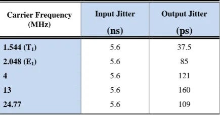
In order to validate the proposed system we first built a circuit model as shown in figure 2. It consists of four dividers (M1, N1, M2 and N2) and two PLLs. The first one is a narrow
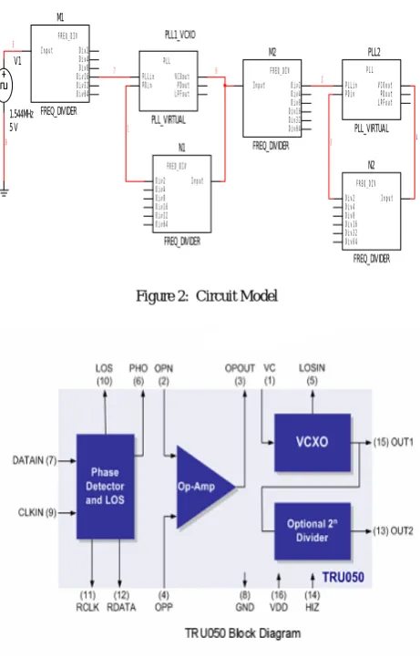
band PLL with a VCXO (TRU050) available from the Vectron international [17]. The block diagram of TRU050 is shown in figure 3. The second one is a wide-band PLL with a VCO (74HC/HCT4046) available from NXP semiconductors [18]. It consists of all parts necessary to make a PLL except for the loop filter components. The programmable frequency dividers needed to complete the dual loop structure are built using Xilinx Spartan XCS10 FPGA.
A major problem in this work was to generate a jittered signal for testing because it is difficult to find an appropriate hardware source that can generate such signal. The problem was overcome by using an FPGA test card which is used for checking LeCroy oscilloscopes (WaveRunner 6100 series). This card can generate various jittered signals that can be used for testing the proposed system. The complete experimental setup of the proposed system is shown in figure 4. Lecroy’s jitter and timing analysis (JTA2) software package is used for the measurement and analysis of jitter.
PLL1_VCXO
PLL_VIRTUAL
PLL
PLLin
LPFout PDin VCOoutPDout
V1 1.544MHz 5 V N1 FREQ_DIVIDER FREQ_DIV Div2 Div4 Div8 Div16 Div32 Div64 Input 1 M1 FREQ_DIVIDER FREQ_DIV Div2 Div4 Div8 Div16 Div32 Div64 Input 5 0 M2 FREQ_DIVIDER FREQ_DIV Div2 Div4 Div8 Div16 Div32 Div64 Input N2 FREQ_DIVIDER FREQ_DIV Div2 Div4 Div8 Div16 Div32 Div64 Input PLL2 PLL_VIRTUAL PLL PLLin LPFout PDin VCOoutPDout
2
3 6
4 7
Figure 2: Circuit Model
Figure 3: Block diagram of TRU050 VCXO based PLL
Figure 4: Experimental setup for jitter measurement
A jittered signal generated using the FPGA test card is fed as an input to the first PLL. A low jittered signal is available at the output. This signal is then fed as an input to the second PLL that is connected in cascade with the first system. The output available from the second system can cover a wide range of frequencies up to 14 MHz.
However, using another PLL with a wider VCO frequency range such as ADF4001 from Analog Devices, it is possible to cover variety of carrier frequencies ranging from T1 (1.544
MHz) to T3 (45 MHz) and E1 (2.048 MHz) to E4 (140 MHz)
[image:2.595.314.542.450.624.2]V. EXPERIMENTAL RESULTS
Four types of measurement were done to measure: 1) Cycle-to-cycle jitter
2) Root mean square (RMS) jitter 3)Accumulated jitter
4)Time interval error (TIE)
The four frequency dividers were built using a 74192 counter plus a D-Type flip-flop to cover wide range of frequencies and 50% duty cycle respectively. We also used Xilinx Spartan XCS10 FPGA based board to modify the value of the dividers. Figure 5 depicts the output signal of the frequency divider with N = 100, measured using a high-speed oscilloscope. The measured jitter in this case is 811 ps as shown in figure 5. For a divider with N = 200, the measured jitter is 5.6 ns as shown in figure 6. Jitter in both the cases is reduced after passing through the frequency dividers.
[image:3.595.332.540.53.167.2]The first PLL circuit was implemented with external components that include resistors and capacitor. The circuit diagram is shown in figure 7. The second PLL (74HC4046) contains all the necessary parts to implement a PLL except for a handful of resistors and capacitors. Resistor of values 10K, 20K and 330K as well as capacitors of capacitances 0.1 µF and 2.2 µF are used. The circuit diagram of the second PLL is shown in figure 8.
[image:3.595.319.536.220.329.2]Figure 7: Configuration of first PLL (TRU050) [17]
Figure 8: Configuration of second PLL (74HC4046) [18]
Figure 5: Jitter measurement for frequency divider (N = 100)
[image:3.595.114.493.387.535.2] [image:3.595.115.492.582.739.2]
Figure 9: Jitter measurement for T1 carrier (1.544 MHz)
[image:4.595.123.484.223.369.2]
Figure 10: Jitter measurement for E1 carrier (2.048 MHz)
Figure 11: Jitter measurement for 4 MHz carrier
[image:4.595.123.484.398.555.2] [image:4.595.122.480.587.754.2]
By applying highly jittered signal to the system and measuring the output jitter at frequency 1.544 MHz (T1
Carrier), we can deduce the jitter behavior of the system .The output from the oscilloscope is as shown in Figure 9, where the upper part represents the carrier frequency. The middle portion of the figure shows the tracking jitter. The lower portion is the jitter histogram. The jitter statistics considered in this paper are cycle to cycle jitter, RMS jitter and accumulated jitter. The TIE has also been measured. TIE measures the position of each edge in a waveform and compares it to the position the edge would have if the waveform frequency was perfect. This analysis can reveal modulation effect, phase noise, and other sources of timing variations. As shown in figure 9, the output jitter is reduced to 37.5 ps as compared to the input jitter which is 5.6 ns.
The same experimentation is done for E1 carrier (2.048
MHz). As can be seen on the left hand side of fig. 10, the carrier frequency (E1), its histogram, tracking jitter and the
jitter histogram are represented from top to bottom. The right hand side of the figure from top to bottom shows another reading of the tracking jitter and the restored carrier frequency respectively. The same jitter statistics are considered here. As shown in figure 10, the value of the jitter was reduced from 5.6 ns in input to 85 ps in the output.
[image:5.595.61.279.432.546.2]The process of jitter measurement was repeated for different values of carrier frequency such as 4 MHz (figure 11), 13 MHz and 24.77 MHz (figure 12). The input and output jitters for different carrier frequencies are summarized in table 1.
Table 1: Jitter measurement summary
Carrier Frequency (MHz) Input Jitter (ns) Output Jitter (ps)
1.544 (T1) 5.6 37.5
2.048 (E1) 5.6 85
4 5.6 121
13 5.6 160
24.77 5.6 109
VI. CONCLUSIONS
PLL is an important module used in mixed signal integrated circuits and systems. It is widely used for clock recovery, data retiming, frequency translation and clock smoothing applications. However, jitter in PLL causes set-up and hold-time violations in digital circuits and this leads to data transmission errors. Hence it is necessary to use jitter-free or low jitter signal source.
In this paper, a low-jitter and wide band dual cascaded PLL system is experimentally verified for different carrier systems such as American (T1-T3) and European (E1-E4). The
recovered clock from the first PLL is jitter bounded due to the effect of the VCXO. The second PLL is a wide frequency band (wide lock-in range) to cover several standard data rates.
The experimental results demonstrate that the jitter behavior is almost directly proportional to the carrier
frequencies ranging from 1.54 MHz up to almost 10 MHz, and then it remains almost constant for frequencies ranging from 10 MHz up to 24.77 MHz. Lecroy’s JTA2 software package is used for the advanced jitter and timing analysis. The experimental result verifies the validity of the proposed system.
ACKNOWLEDGMENT
The authors would like to thank Prof. Dr. Mohammed Abou El Ela (King Saud University), Dr. Jim Noras (University of Bradford) and the staff of Research center, College of Engineering, King Saud University for their support.
REFERENCES
[1] A. Mann, A. Karalkar, L. He and M. Jones, “The design of a low-power low-noise phase lock loop,” in Proc. of 11th Intl. Symp. on Quality Electronic Design (ISQED), pp. 528-531, 2010.
[2] Y. K. Some and P. Y. Kam, “Bit error probability of QPSK with noisy phase reference,” IEE Proceedings-Communications, Vol. 142, No. 5, pp. 292-296, 1995.
[3] W. E. Thain Jr. and J. A. Connelly, “Simulating Phase Noise in Phase-Locked Loops with a Circuit Simulator,” in Proc. of IEEE Intl. Symp. Circuits and Systems, Vol. 3, pp. 1760-1763, 1995.
[4] “Jitter in PLL-Based Systems: Causes, Effects and Solutions,” Cypress Semiconductor Corporation, 1997.
[5] P. Heydari and M. Pedram, “Analysis of Jitter due to Power-Supply Noise in Phase-Locked Loops,” in Proc. of IEEE Custom Integrated Circuits Conf., pp. 443-446, 2000.
[6] F. Herzel and B. Razavi, “A study of Oscillator Jitter Due to Supply and Substrate Noise,” IEEE Trans. on Circuits and Systems II: Analog and Digital Signal Processing, Vol. 46, No. 1, pp. 56-62, 1999. [7] D. H. Wolaver, Phase-Locked Loop Circuit Design, Prentice Hall,
Englewood Cliffs: New Jersey, 1991.
[8] R. E. Best, Phase-Locked Loops: Design, Simulation, and Applications, McGraw Hill, New York, 2007.
[9] A. Telba, S. M. Qasim, J. M. Noras, B. Almashary and M. A. El Ela, “Behavioral Modeling and Simulation of Dual Cascaded PLL Based Frequency Synthesizer,” Journal of Active and Passive Electronic Devices, Vol. 4, No. 4, pp. 321-334, 2009.
[10] A. Hajimiri and T. H. Lee, “A General Theory of Phase Noise in Electrical Oscillators,” IEEE Journal of Solid-State Circuits, Vol. 33, No. 2, pp. 179-194, 1998.
[11] M. Kihara, S. Ono and P. Eskelinen, Digital clocks for synchronization and communications, Artech House, 2003.
[12] T. Pialis and K. Phang, “Analysis of Timing Jitter in Ring Oscillators Due to Power Supply Noise,” in Proc. of IEEE Intl. Symp. Circuits and Systems (ISCAS), Vol. 1, pp. 685-688, 2003.
[13] P. Heydari, “Analysis of the PLL jitter due to power/ground and substrate noise,” IEEE Trans. on Circuits and Systems I: Regular papers, vol. 51, No. 12, pp. 2404-2416, 2004.
[14] K. M. Ware, H.-S. Lee, and C. G. Sodini, “A 200-MHz CMOS phase-locked loop with dual phase detectors,” IEEE J. Solid-State Circuits, vol. 24, No.6, pp. 1560-1568, 1989.
[15] W. S. T. Yan and H. C. Luong, “A 2-V 900-MHz monolithic CMOS dual-loop frequency Synthesizer for GSM receivers,” IEEE Journal of Solid State Circuits, Vol. 36, No. 2, pp. 204-216, 2001.
[16] AN-531, “DART Dejitter PLL Design and Analysis” Application note, TranSwitch Corporation, 2004.
[17] TRU050, http://www.vectron.com/products/fxcdr/tru050.pdf [18] 74HC HCF4046B is a COS/MOS Micro power Phase-Locked Loop
(PLL) consists of a low-power, linear voltage-controlled oscillator (VCO) and two different phase comparators having a common signal-input amplifier and a common comparator all information in- .http://www.nxp.com/documents/data_sheet/74HC_HCT4046A_CNV .pdf
[19] ADF4001: 200 MHz clock generator PLL
![Figure 7: Configuration of first PLL (TRU050) [17]](https://thumb-us.123doks.com/thumbv2/123dok_us/1298393.659292/3.595.115.492.582.739/figure-configuration-pll-tru.webp)