2019 south ritchey street · santa ana, caHfornia 92705 · (714) 558·82TI
CAL DATA 100 ENGINE
(P/N C81080180 AND C81080190) TECHNICAL MANUAL
C21518008-XO
DOCUMENT C21518008
Revision XO January 1975
. cal Data, MACROBUS, QUADBOARD and HEXBOARD are trademarks of California Data Processors.
The inf orination herein is the property of California Data Processors. Transmittal, receipt or possession of the
in-formation does not express, license or imply any rights to use, sell or manufacture from this information and no re-production or publication of it, in whole or in part shail
be made without written authorization from an officer of° .. ;·~--.
the above finn. · ·.· ., , ..
·~
...
·©
copyri'ght 1975california data processors
.$15;oo
REVISIONS
Revision Date Approval Description
XO 3-75 Preliminary
The revision history of each page in this document is indicated below:
Page i i i iii 1-1 1-2 1-3 1-4 2-1 2-2 2-3 2-4 2-5· 2-6 2-7 2-8 2-9 2-10 3-1 3-2 3-3 3-4 4-1 4-2 4-3 4-4 4-5 4-6 4-7 4-8 4-9 4-10:· 4-<U 4"."'"t2 4-1,3 •.',•· '.,,.. Revision XO v
v
v
.,.v
v
vv
v
Page 4-14 4-15 5-1 5-2 5-3 5-4 5-5 5.:...6 5-7 5-8 5-9 5-10 5-11 5-12 5-13 5-14 5-15 5-16 5-17 5-18 5-19 5-20 5-21 5-22 5-23 5-24 5-25 5-26 5-27 5-28 5-29 5-305-F.
5-32 Revision XO vv
v I / v v~ v • /v
v' Revision Page XO5-33
v
5-34 \ /
5-35 v
5-36
v
5-37
v
5-38 V"
5-39
v
5-40 v
5-41 I /
5-42 ,_.,.,..
5-43 v
5-44 v
5-45
v
5-46 v
5-47 v
6-1
v
A-1 v
A-2
v
A-3
v
B-1 v
C-1 v
C-2 v
C-3
v
C-4 v
C-5 v
C-6 \.."
C-7
v
C-8
v
..
SECTION 1: INTRODUCTION 1.1
1.2
SCOPE. . . .
DOCUMENTATION. . . • .
1.2.1 Publications . . . . . 1.2.2 Engineering Drawings . • . • . 1.2.3 Abbreviations and Conventions . . SECTION 2: DESCRIPTION
2.1 2.2
2.3
2.4 2.5
OVERVIEW . . . . . SYSTEM ORGANIZATION. . 2.2.1 Engine .
2.2.2 Microbus . . . • . . 2.2.3 MACROBUS Channel Adapter 2.2.4 Macropanel • . .
2.2.5 Microconsole . . . . . . 2.2.6 Magnetic Core Memory .
2.2.7 Peripheral Devices • . FIRMWARE DEVELOPMENT AIDS . . 2.3.1 Alterable Control Memory . 2.3.2 Support Software •
FEATURES . . • • . . . . SPECIFICATIONS
SECTION 3: PHYSICAL DESCRIPTION 3.1
3.2
SYSTEM HARDWARE . . ENGINE BOARDS. SECTION 4: ENGINE 4.1
4.2
4.3
FUNCTIONAL DESCRIPTION
CONTROL SECTION . . . • .
4.2.1 Control Memory (CM) • . . . 4.2.2 Location Counter (CC).
4.2.3 Microcommand Register (CR) . . . . 4.2.4 Control Stack (CS)
4.2.5 Loop Counter (LC) . • . DATA SECTION . . . .
4.3.1 File Registers (FR). . . . . . 4.3.2 Operand Buses (AB, BB) . . . . . 4.3.3 Arithmetic/Logic Unit (AU)
··4. 3. 4 AU Shift Elements (SX) and Shift Register (XR) :'. .• .4.3;.5 M 1:3US (MB) . . . . • . . . . .
4.3.6 Microcondition Codes . . . . . . . 4.3.7 Microstatus Register (MS) . .
, " 4. 3.8· Word and B~te Operations . . • . . .
C21.5180QS~XO
CONTENTS
. .
:. . .
.
l"".'l 1-1 1-1 1-1 1-3 2-1 2-1 2-1 2-1 2-1 2-4 2-4 2-4 2-4 2-5 2-5 2-5 2-5 2-7 3-1 3-3 4-1 4-5 4-5 4-7 4-8 4-9 4_:9,~ 4,~9 4~~1 ~-11 4-11 4-12\ J ~
4.:-;-12
SECTION 5: MICROCOMMANDS 5.1 5.2 5.3 5.4 5.5
GENERAL. • • . • . •
MICROCOMMAND CLASSES • • . . • • . • • • 5.2.1 Logical and Arithmetic Classes • 5. 2. 2 Special Class. . • • • • . LOGICAL MICROCOMMANDS • • .
5.3.l Emulate (Optional) 5.3.2 Sign Extend A • • • • . 5.3.3 Move A • • .
5. 3 • 4 Move B . • . . 5.3.5 Complement A 5.3.6 Complement B . 5.3.7 AND A, B . 5.3.8 AND A, B .
5.3.9 AND A, B . • • • • 5.3.10 Not OR . .
5.3.11 OR A, B. • . . . . 5.3.12 OR A, ~ . . . • • . 5.3.13 OR
X,
B . . . . .5.3.14 Not AND . . . 5.3.15 Exclusive OR 5.3.16 Coincidence . .
ARITHMETIC MICROCOMMANDS . • . • . 5 • 4 . 1 Add A, B . . • . . . • . • 5.4.2 Subtract A, B • .
5.4.3 Add Carry . . . 5.4.4 Subtract Carry . 5.4.5 Increase A . . 5.4.6 Decrease A . . . 5.4.7 Add A Masked . SPECIAL MICROCOMMANDS • •
5.5.1 Shift. • • • . .
5.5.2 5.5.3 5.5.4 5.5.5 5.5.6 ?" _5. 5r7
5.5.1.1 Single-Precision Shifts. Multiply Step. •
Divide Step. • . . • • . . Test Bit . . • . . . . • • Modify Macrostatus (Optional).
Conditional Memory Access (Optional) . . • . Decode (Optional) • . . . • . • .
.(
SECTION';6:'·; MAINTENANCE 6.1
6.2 6.3
i i
· . GENERAL. . . :~ . • . •
PREVENTIVE MAINTENANCE . . CORRECTIVE ··MAINTENANCE .
APPENDICES
APPENDIX A: ENGINE ARITHMETIC A.l
A.2
A.3
NUMBER REPRESENTATION • • ADDITION • • •
SUBTRACTION.
APPENDIX B: FIXED MEMORY ASSIGNMENTS APPENDIX C: CONNECTOR PIN ASSIGNMENTS
Table 1-1 2-1 4-1 5-1 5-2 5-3 5-4 B-1 C-1 c....:2
C-3
c-4
C-5 .·
c-6·.-:· C-7u·· c-a:". Figure 1-1 2-1 2-2 '3-1 "~-2 4·".'"~ TABLES Title
Abbreviations . • • • • • • • • • • • Cal Data 1 Computer Specifications • • • • Microstatus Register Bit Definitions. Cal Data 100 Engine Microcommand Summary.
Microcondition Codes for Logical Microcommands. • • • • • Microcondition Codes for Arithmetic Microcommands •
SO-Field Shift Specification. • • • • • • • • • Interrupt Vectors • • • • • • . • • •
Connector A Pin Assignments, MACROBUS • Connector B Pin Ass.ignments, MACROBUS
Connector C Pin Assignments • • • • • • • • • • • • • • • Connector D Pin Assignments • • • • • •
Connector E Pin Assignments • Connector F Pin Ass.ignments Connector Jl Pin Assignments. Connector J2 Pin Assignments.
ILLUSTRATIONS
Title
.
.
-·~.
.
Relationship of Publications to Cal Data 1 System Elements. • • • • • • Cal Data 1 Computer System with Memory Ma~agement Unit, 128K
Words of Cal Data 16Kl6 (850-ns) Core Memory and Serial I/O
Control;Ler. • . • . • • • • . • • • • • • • • • • • • • .., ..• :.;•·.~·.-··.
Cal Data 1 Computer System Organization • • • • • • • • • ". • • · • Cal Data 1 Computer with Boards Installed (Fan Panel is She~ DQWn) · ·• Cal Data 100 Engine Board Configuration • • • • •
Cal Data 100 Engine Block Diagram • • • •
. .
...
A-1 A-2 A-3 1-4 2-7 4-13 5-5 5-7 5-13 5-20 B-1 C-1 C-2 C-3 C-4
c-s
C-6c-7
C-8 1-2 2-2 2-3 3-2 3-4·4-2
1 4-2 4~3;4..;4·
Cal Data 100 Engine .Interface with the Microbus
Cal Data 100 Engine Control Section Block Diagram • ~ • ·•
•• r;t4-4
.···.X<..:~-6
·s····.1, .. ::
' -.J..·1
' . ' ~ .
Cal Data 100 Engine Data Section Block Diagram. • • • • • • •• Microcommand Formats. • • • • • . • • • • • • • •
c2isiaooa-xo ·
.. .···~
,•
.
;;..
'4:-,£.Q::
5-~· ·.
SECTION 1
INTRODUCTION
1.1 SCOPE
This manual provides the information needed to understand and maintain the Cal Data 100 Engine, part numbers C81080180 and C81080190, when used with the drawing package provided. The information in this manual is for the use of a skilled technician familiar with standard test equipment, solid-state logic theory, common maintenance
practices and standard troubleshooting techniques. A basic knowledge of design principles and circuits used in small computers is assumed, hence no tutorial material of this kind is included.
As a stand-alone publication, this manual has a good functional and physical description of the Cal Data 100 Engine, providing the
information needed to understand the capabilities and features of the computer and to plan a system using it. The maintenance coverage of this manual is commensurate with the prerequisite skills and
knowledge of the defined user, characteristics of the product and maintainability requirements established by Cal Data. ·
1.2 DOCUMENTATION
1. 2.1
1. 2. 2
This manual describes the engine of a Cal Data computer system that is equipped with a MACROBUS Channel Adapter (part number C81080300)
and an Emulate Board (part number C81080210).
The following paragraphs define publications and conventions that support this manual.
Publications
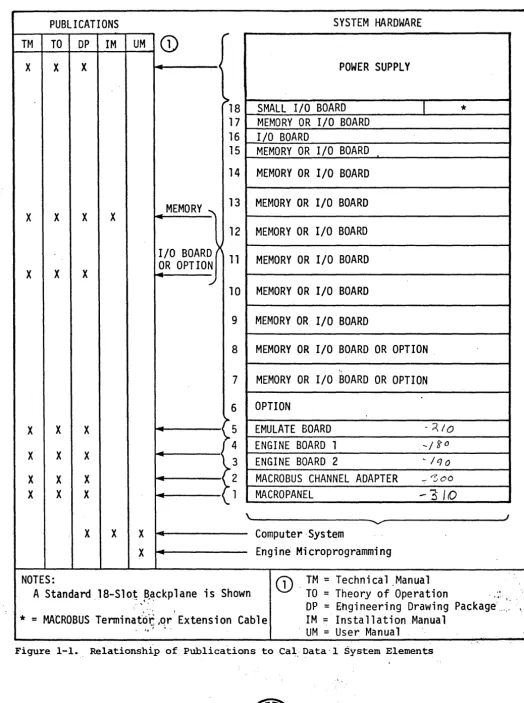
Figure 1-1 illustrates the relationship between Cal Data system elements and technical publications. Controlled copies of publications,
provided in accordance with the terms of the purchase contract~ are kept current for the life of the product.
Engineering Drawings
For maintenance purposes, this manual is supported by a drawing package that contains schematic diagrams, assembly drawings and other required engineering drawings. The drawing package is updated with the
latest revision of each drawing.
PUBLICATIONS
SYSTEM HARDWARE
r
I
TM
TO
DP
IM
UM
Q)
x
x
x
x
x
x
x
x
x
x
x
x
x
x
NOTES:
x
x
x
x
x
x
x
x
x
x
-
POWER SUPPLY
18
SMALL I/0 BOARD
17
MEMORY OR I/0 BOARD
16
I/0 BOARD
15
MEMORY OR I/0 BOARD
14
MEMORY OR I/0 BOARD
...._MEMORY
~13
MEMORY OR I/0 BOARD
-12
MEMORY OR I/O BOARD
I/0 BOARD )( l l
OR OPTION
.
MEMORY OR I/0 BOARD
10
MEMORY OR I/0 BOARD
9
MEMORY OR I/O BOARD
I
8
MEMORY OR 1/0 BOARD OR OPTION
7
MEMORY OR 1/0 BOARD OR OPTION
6
OPTION
.l>-5
.... ~1---<
EMULATE BOARD
-
~ Io*
1---c
4
ENGINE BOARD 1
.... ;
8' o-
-
3ENGINE BOARD
2 .._ I qo
.... ~i---< 2
MACROBUS CHANNEL ADAPTER
- ":) C'>O--
1
MACROPANEL
-3
ltO
\. ..J
x
--
-
Computer·System
x ....
~1---Engine Microprogramming
TM
=
Technical _Manual
A Standard 18-Slot Backplane is Shown
• . '.~ '\, ~ : I
CD
TO
=
Theory of Operation
.:'.
DP
=
Ehgi neeri ng Drawing Package: ... ~.'
·,,.
IM
=
Installation .Manual
*
=
MACROBUS Tenninat'6t·
1Qr1
Extension Cable
JA, ' '
[image:10.618.57.581.49.752.2]· UM
=
User
Manual
Figure 1-1.. Relationship of Publications to Ca~:Data·l System Elements
..
..
1. 2. 3 Abbreviations and Conventions
C21518008-XO
Tallle 1-1 lists the abbreviations foun.d in this manual. Conventions used in the text of this manual include:
a. Equipment panel nomenclature is reproduced in all upper-case characters.
b. The proper names of instructions, microcommands and signals are capitalized.
c. ZERO and ONE are used to express binary logic
"O" and "l" states, respectively.
d. Hexadecimal numbers are preceded by a dollar sign for easy identification.
e. A colon is used to indicate a range of bits. For example, the range of address bits Al2 to A03 is written Al2:A03.
Table 1-1. ·Abbreviations Abbreviation
Cal Data CPU MCA I/O LFC RAM ROM PROM MSI LSI MMU LED ACM DMA CM cc CR cs SC LC MB FR AB BB AU sx PS LR RR IR XR ER EIA c .v z n p d 1-4 Meaning
California Data Processors
central processi.ng unit (engine)
MACROBUS Channel Adapter input/output
Line-Frequency Clock random-access memory read-only memory
progrannnable read-only memory
medium-scale integration large-scale integration Memory Management Unit light emitting diode Alterable Control Memory direct memory access control memory
microcommand location counter
microcommand register control stack
stack counter loop counter
M bus (data destination bus)*
file register ' A-operand bus*
B-operand bus*
arithmetic/logic unit AU shift elements
processor (macro)status register
stack-limit register data-read register instruction register shift.register
emulate decode register emulate instruction address carry out
microcondition code overflow
microcondition code zero data-value
(microcondition) code negative ;~data-value
(mic~o-cQndi tion) code
positive Ciata-value (microcondition) code odd data-value
(microcondition) code
Abbreviation MS L
v
z
N p D cps cpm lpm K max min A ac de nnsv
ns ... Hz oc cm
Meaning
microstatus register MS register
link bit MS register
overflow bit
MS register
zero data-value bit MS register
negative data-value bit
MS register positive data-value bit MS register odd
data-value bit
characters per second cards per minute
l~nes per minute l,024(address or
memory locations) maximum
minimum ampere
alternating current direct current root-mean-square volt
nanosecond hertz
degrees celsius centimeter
* =
part of the main Microbus [image:12.617.56.589.63.739.2]SECTION 2
DESCRIPTION
2. 1 OVERVIEW
The Cal Data 1 Computer (Figure 2-1) is a high-speed microprogrannned digital computer designed for application in a wide variety of computing and control applications. Microprogrannning, combined with a powerful · and flexible hardware architecture, centering around the Cal Data 100 Engine and Microbus, permits the basic computer to be fully optimized to a specific application. The Cal Data 100 Engine is designed primarily for efficient, high-speed emulation of general-purpose computer archi-tectures. It can also be applied as a direct function processor by im-plementation of problem-oriented microprograms.
2.2 SYSTEM ORGANIZATION
2.2.1
2.2.2
The overall system organization is shown in Figure 2-2. The system consists of a set of hardware and software elements that can be utilized in a wide variety of applications. A brief description of the elements of the computer system is given below. Details are given in other sec-tions of this manual and in supporting manuals.
Engine
The central element of the system is the ~ngine (CPU), divided into con-. trol and data sections, and controlled by microprogram sequences (firm-ware) stored in a control memory. By changing the contents of control memory, the entire operation of the system can be altered. An emulation system is implemented by placing appropriate firmware in control memory, causing the CPU to operate like the computer being emulated.
The control and data sections contain the internal arithmetic/logic cir-cuits, data paths, registers, control logic and timing circuitry of the machine. The CPU communicates with the rest of the system via the Microbus.
Microbus
The Microbus is a universal bus that is the main connnunication and con-trol channel of the system. The Microbus transmits data and control in-formation between the CPU and all elements of the system.
The Microbus can be conditioned by one or more I/O channel adapters to interface with a wide variety of I/O devices obeying specific interface rules. The primary I/O channel adapter o~ the Cal Data 1 system is the Cal Data 1 MACROBUS Channel Adapter.
MACROBUS Chagnel Adapter
~ ·~
The MACROBUS Channel .Adapter (MCA) provides data, address and control circuitry for parallel I/O operations in the system. The McA frees the
Figure 2-1. Cal Data 1 Computer System with Memory Management Unit, 128K Words·. of Cal D~.!:a 16KX16 (850-ns) Core Memory and Serial I/O Controller
! .
[image:14.621.50.564.71.634.2]MACRO BUS
TERMINATOR:
MACRO PANEL
MACR~BUS
CHANNEL ADAPTE
.,.__ _ _ _ _ M _ _ _ _
__.
MEMORY--MANAGEMENT
_!l_N!L _ _
ENGINE
BOARD 1
ENGINE
BOARD 2
R
t
Jc
A
R
0B
u
s
1.,..,-1EMULATE
BOARD
---M---11
...._ _ _ _ _ A _ _ _ _
__.
MICROBUS
----,
MICROCONSOLE
_j.
---,
SPECIAL
I
FUNCTIONS
_j
-lt"o~HANNa
I
ADAPTER #N
_j
-,-,---L.-1
1/0
CHANNEL #N
. COMMUNICATION
·CHANNEL AND
INTERNAL CONTROL
·~OTE:
- - =Optional
c
R0
B - - - -.. ---11
u---11
s
MACROBUS
TERMINATOR
'.f
igJ;~
2-2. Cal Data 1 Computer SystemOrgan~zation
C2151800S-XO
SERIAL 1/0
CHANNEL
t
5E°RIAL
l/o-i_J
CONTROLLER
_j
-MEMORY
PERIPHERAL
CONTROLLER
•
•
•
PERIPHERAL
CONTROLLER
---,
SYSTEM
I
INTERFACES
_J
-2.2.4
2.2.5
2.2.6
2.2.7
central Microbus for very-high-speed communication between the CPU and other Microbus devices, and can permit I/O channel devices to communicate directly with each other, independently of the CPU.
Macropanel
A Macropanel, representing the control panel of a general-purpose com-puter, is often provided in an emulation application. The Macropanel is serviced by the CPU as an I/O device interfacing with the MACROBUS.
Special support firmware is provided for the Macropanel. The primary Macropanel for the Cal Data 1 system is the Cal Data 1 Macropanel. Microconsole
A Microconsole is available to provide microlevel control and display for checking out and debugging firmware, and also for various mainten-ance and troubleshooting procedures. The Microconsole consists of a remotely mounted Micropanel and a plug-in Micropanel ~ontrol board that permits the user to exercise direct control over· the CPU. Facilities are provided to construct full microcommands, to display microcommands and to execute microconunands on a single-step or "trap-mode" basis. The Microconsole also contains 32 words of alterable control memory that can substitute for equivalent blocks of CPU control memory.
The Microconsole can be used in conjunction with the Macropanel and is useful for initial debugging of new firmware as well as for on-line troubleshooting of computer hardware, but is usually not required in an applied system configuration.
Magnetic Core Memory
Cal Data core meIOC>ry comprises modular blocks of SK (8,192) or lGK 16-bit words, each contained on a single circuit board. Each module plugs directly into the MACROBUS and is treated as an I/O device in the system. The maximmn normal system capacity is 128K words. Two identi-cal modules can be interleaved to achieve an increased effective through-put rate on the MACROBUS.
The MACROBUS can accommodate memory devices other than magnetic core, such as semiconductor ROM or RAM modules.. The only requirement is that such units obey MACROBUS use rules. Modules of varying size and speed can be freely mixed with core memory. OMA-type MACROBUS devices may communicate directly with memory.
Peripheral Devices
Peripheral device controllers and system interfaces are attached to the MACROBUS as shown,; in Figure 2-2. The user can readily interface devices ·;."·.with'tthe MACROBQS .. 'Using simple design rules. Cal Data offers I/O channels ·· .. su~h as tne MACRbBUS with different structures as well as several. ~itandard
periph~r~l "sub'sy'stems to enhance user applications.' The subsyste~s ·. ·
offer~d 'to" support· normal progranuning and system development operations· ·
·are:
a. Paper Tape Reader. High-speed photoelectric reader, 300 characters per second, fanfold tape.
b. Paper Tape Punch. High-speed punch, 75 characters per second, fanfold tape.
c. Card Reader. High-speed photoelectric card reader, 300 cards per minute with code conversion in the controller. d. Line Printer. 80- or 132-column printer, 125 or 200
lines per minute. e. Memory extensions.
2.3
FIRMWARE DEVELOPMENT AIDS
2.3.1
2.3.2
2 •. 4·
Cal Data offers specialized hardware and software elements to aid users in developing custom firmware. These are briefly described below.
Alterable Control Memory
Alterable Control Memory (ACM) is a modular plug-in unit that contains increments of 256 words of electrically alterable control memory. The ACM also contains alterable elements associated with instruction emula-tion and decoding.
With the ACM, a programmer can load or read the contents of control memory directly and execute trial firmware code at normal processor execution speeds. The ACM is particularly useful for dynamic system tests where external real-time events must be considered to fully eval-uate a firmware microprogram. The ACM is supported by a software oper-ating system that permits the programmer to use a teleprinter to control the system.
Support Software
The following software is available to support firmware development: a. Symbolic Microassembler. This program is a complete
symbolic assembler that permits convenient coding and listing of microprograms. It is written in Cal Data 135 emulator language and can be run on any Cal Data 135 or compatible computer having the required memory con-figuration.
b. ACM Software Operating System. This program is designed to provide operational control over execution of firm-ware in the ACM. It requires that the Cal Data 135 emulator be resident in control memory.
FEATURES
The Cal Data computer architecture combines general microprogranuning capability with specialized optional features. to permit higp emu.lation
' . . ' ' ' ~ .
speeds with efficient control-memory space utilization. The~· meCnanical design used prov~des full modularity, mounting ii.~xibi'l:i:t;:y' .and service convenience. Cooling, power distribution arid dtllefr · crl.tlcal system re-quirements are optimized for OEM applications~ Conser'7ati ve el.ectrical "implementation ensures wide margins, readily available components and
reliable operation over a.wide environmental range. Subassemblies are
... .'Ir , ;'2.~6.
des_igned for easy assembly and automated testi_ng, and the overall system is structured for simple, straightforward manufactur~ng procedures. Basic des_ign features of the Cal Data computer system are:
• 48-bit microconunand word length
• Parallel execution of multiple functions per microcommand • 165-ns microcommand execution time
• 16-bit data word length
• 16 multipurpose file registers (16 bits each)
• Nine additional registers accessible by microcozmnand • 16-level hardware pushdown stack
• Microcommand sequence repeat loop counter
• Optional high-speed emulation instruction decode, function generation and interrupt-response hardware.
• Bit, byte and word manipulations
• 256- to 4096-word control memory using bipolar ROM or PROM devices • Power-failure/restart circuitry and line-frequency clock included
in the computer
• Unique, control memory substitution provisions
• Optional Multiply, Divide, and single- and double-precision Shift micro commands
• Hardware microprogram interrupts Input/Output and Memory
• Universal asynchronous I/O channel with direct-memory-access capability
• Four external priority interrupt levels • 16-bit parallel· word or byte-mode transfers • Automatic I/O channel delay time-out protection • Optional asynchronous serial I/O channel
• BK-word (675-ns cycle, 275-ns access) and 16K-word (850-ns cycle, 300-ns access) core memory modules
e Interleaved data transfers between identical memory modules
• Optional extended addressing feature for addressable memory expan-sion to 31K without memory management
• Expansion to 124K or 127K of directly addressable memory with optional. Memory Management Unit
Microprogramming Aids • Microconsole
• Alterable.Control-Memory and support software • Symbolic . .Microassembler
Packaging, Pbwer and Environmental • . 10~ inch coinputer chassis
~.-'•,. ,~;~>:P:finted-c;i.rcui .. . •.-:;·.: ,,. t backplane
·;
with vertical board mounting from the top with up to 13 spare slots for memory and
:> ...
·~:.~,(...Q~6P. .. 'l.t:ro.~ler boards. •, .'Fd'ui:W';6ans" for high-volume, positive-pressure q.ir
· 'cih'cl:S~i~~·rwith provision for air filters ._·~ .. ,
Modulaf~ p0wer supply providing 36 A at +5 Vdc
flow throuqh the
•
• Low-noise internal power distribution and grounding system • Convenient external I/O cabling
• Extension chassis available
• System designed to meet UL standards • O to +5o0
c
ambient operating temperature• 10 to 90% relative humidity (without condensation) Electrical and Electronic
• Bipolar TTL integrated circuits (multisourced) • Extensive use of MSI and LSI
e Wide timing margins
• High noise immunity I/O drivers and receivers • Single-phase clock
• Conservative component derating
• Metal can transistors and hermetically-sealed passive devices only
2.5
SPECIFICATIONS
.General specifications for the Cal Data 1 Computer are given in Table 2-1. Table 2-1. Cal Data 1 Computer Specifications
. _': C2?5:1'8008~X6
Characteristic TYPE
CONTROL
Microconunand length Execution rate
Microcommand classes
Special operations
Conditional skip/branch
Fixed control memory . ·Alterable control . _memory
Specification
High-speed microprogrammed digital com-puter designed for efficient emulation of general-purpose computer architectures and for direct custom applications
48 bits
165 ns, min.; 330 ns if skip or branch is made; clock rate is adjustable 8 arithmetic
16 logical 8 special
Special microcommands include double-precision Shift, Multiply-Step and
Divide-Step ·
Each microcommand wi,th conditional skip or branch capabilit:Y"r ~ests on either current {dynamic) c.onditions or
on previous {static} conditions
Bipolar ROM or PROM; 4, 096.,.wqrds, max
- . ':L .
~ .~
?:.'.:'._:f ...
·:'.:~y
/
Bipolar RAM; 512 .wor~r ~·'..without .
auxiliary power;
i,'s§6:tf;;d:ids·
max ·with·.-· ..• • '' l'." .; • . - '
[image:19.612.63.563.310.768.2]Table 2-1. (Continued) Characteristic
Control memory stack Emulation enhancement
Loop counter
Interrupts
PROCESSING Word length Arithmetic/logic
Registers
INPUT/OUTPUT (TYPICAL) Type
~.·:.< I;)at·a
' :. '' ~-... .-·
Specification
16-level hardware pushdown stack
Special emulation decode tables provide automatic addresses to control memory microroutines for high-speed program execution
Eight-bit counter for single or multi-instruction repeats
Multilevel priority-interrupt structure provides automatic addresses to control memory microroutines for internal and external conditions
16 bits
Both word and byte operations are pro-vided; fixed point, one's or two's complement arithmetic; arithmetic condition codes are carry (link) , over-flow, negati:_ve, zero, positive, odd;
arithmetic~and logical shifts (multibit
using loop counter for repeats are provided)
Eight or sixteen 16-bit multipurpose files (FR)
Shift register (XR)
Microstatus register (MS) Instruction register (IR)* Decode Register (ER)*.
Processor (macrolevel) status register (PS)*
Asynchronous bidirectional I/O channel derived from the Microbus; requires I/O channel adapter; handles communications between CPU, memory and peripheral elements
16 bits with byte capability
16 bits from Microbus (can be.extended within I/O channel adapter);ieast-significant bit is for ~yt{addressing
.. } i.,
*Part of emulation enhancement circuitry .,i
·1.
'. ~. ,,.·,. [image:20.613.57.562.78.725.2]Table 2-1. (Continued)
'c21518008-Xff
Characteristic
I/O channel priorities and requests
Serial I/O channel
Memory
Memory expansion
Memory interleave
Line-frequency clock
PACKAGING
Processor chassis
Connectors
Board size
POWER
AC input·
Specification
Four priority-request levels with multiple requests per level;
nonprocessor request (NPR) level for direct device-to-device transfers; CPU can set its own priority to any level except NPR
Serial I/O controller (option) for rates up to 9600 baud; RS-232 or cur-rent-loop interface
Magnetic core; SK or 16K words per module; 16 bits per word
Typically, 124K words maximum; Memory Management Unit (option) is required above 32K
SK-word or 16K-word Cal Data core mem-ory pairs can be interleaved for in-creased throughput rate
50/60 Hz line clock
10~ inches (26.7 cm) high by 19 inches (4S cm) wide by 24 inches (43 cm) deep; rack-mounted (slides) or table-top; vertical, top-loaded boards; contains Macropanel, Engine, MCA plus slots for memory and I/O controllers; internal power supply; cooling fans; internal power distribution
36-pin, 0.6 inch (1.5 cm) card inser-tion depth; mounted on printed-circuit backplane
S.9 by 15.7 inches (22.7 by 39.9 cm); six connector positions (216 pins) on long edge
j
115/20S/230 Vac, 50 or 60 Hg
. ·~'/·
• I ·~ • ~~'~·~\~ ),~~~<·•
[image:21.613.73.566.74.764.2]2~10 "
Table 2-1. (Continued) Characteristic
Power monitor
ENVIRONMENT Temperature Humidity
CIRCUITS
Integrated circuits
Discrete devices
Internal logic levels I/O logic levels MICROPROGRAMMING SUPPORT HARDWARE
Microconsole
Alterable control memory (ACM)
MICROPROG~ING
SUPPORT SOFTwARE/ FIRMWARE
Symbolic·· micro-assembler ' ACM software operating system
Specification
Unregulated: -22 Vdc, 1.5 A +8 Vrms, 1.5 A
Power-failure/restart signals to CPU for automatic shutdown and restart operations
o
0 to·+so0c
ambient temperature10 to 90% relative, without condensa-tion
Bipolar TTL; extensive MSI and LSI usage
Metal-can transistors; hermetically sealed components only
ZERO = 0 Vdc; ONE = +5 Vdc, nominal ZERO
=
+3.4 Vdc, nominal; ONE=
0 VdcProvides direct control over Engine; microcommand entry and display; single-step and trap-mode micro-comrnand execution
Modular 256-word increments of control memory that can be loaded and read; operates CPU at full execution speed
Symbolic assembler for microprogram coding and documentation
[image:22.617.79.559.64.755.2]SECTION 3
PHYSICAL DESCRIPTION
3.1
SYSTEM HARDWARE
C21518008-XO
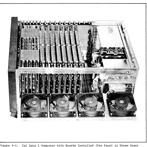
All Cal Data Engine and system elements are modular and can be mounted in a standard chassis (Figure 3-1) that occupies 10.5 inches (26.7 cm) of a 19-inch (48-cm) RETMA rack. This modularity gives the user maximum flexibility in system design and configuration.
The standard computer chassis dimensions are: 10.4 inches (26.5 cm) high
19.0 inches (48.3 cm) wide 24.0 inches (61.0 cm) deep
Hardware items included with the standard computer chassis are: a. Chassis box with backplane
b. Top and bottom covers
c. Hinged fan panel and four fans d. Chassis slides
e. Macropanel bezel and overlay
A power supply mounts at the rear of the chassis. The ac power cord exits from a control panel accessible at the rear of the chassis. This panel also has the ac line switch, fuses, convenience outlet (115 Vac model only) and Macropanel lock switch.
The four fans provide horizontal, positive-pressure air flow across the vertical computer boards and power supply. The fan panel is hinged to permit moving the fans when boards are removed or installed.
System electronics are mounted on modular printed-circuit boards that insert vertically through the top of the chassis into connectors mounted on the backplane in the bottom of the chassis. The backplane provides printed-circuit (and wire-wrap) connections between all boards.
Device controller cables are generally connected at the top edge of I/O
boards by means of flat cable. These cables a¥e routed over the top of the boards and exit via a cutout at the top'.. rear of the chassis. A strain-relief clamp is provided. All standard Ca1:Data I/O
and memory boards have provision for this cable routing scheme. The backplane contains up to 18 connector rows ~bo~rd slots).
The Macropanel is mounted on a printed circuit board that plugs into the first connector row of the backplane. The Macropanel is covered by·':··an, overlay held in place by the bezel. The bezel and over.l,ay ·are · · · removable.from the front when the chassis is install~d :i;n~~ ra9k.
3.2
ENGINE BOARDS
The Engine comprises two boards labeled Engine 1 (part number C81080180) and Engine 2 (part number C81080190). Each Engine board (Figure 3-2) is a hex-width board 15.7 by 8.9 inches (33.9 by 22.7 cm). Engine 1 nonnally plugs into slot 4 of the cal Data computer chassis.~ Engine 2 nonnally plugs into slot 3. The right-hand edge of each b~ard has a 1.0 by 5.5 inch (2.5 by 14.0 cm) cutout as clearance for the side-mounted cooling fans in the chassis.
There are six printed-circuit connectors (A to F) on the bottom edge of each board, and two (Jl and J2) on the top edge. Connectors A.and B interface with the MACROBUS. Connectors
c
to F, and Jl and J2 inter-face with the main computer Microb.us~ , Connectors A to F are standard backplane connectors. Connectors Jl and J2 plug into the two small processor-interconnection boards.There are no controls or adjustable elements on the Engine.
*Because· of tjl~ universal connections in the CPU area of the chassis, the Engine .. boards . can op~~ate ; in any slot from 1 to 5.
15.69"
Al
A3o---
Al
a
J2a
a
COMPONENT SIDE
FVl
FAl
EVl
EAl
DVl
DAl
CVl
CAl
BVl
·®Solder Side
=
Bl to
830.
Likewise with connector.J2 •
0.99"~
©
Jl
l-an an
.
an 'd'°'
ClO.
BAl AVl
CD
AAl
.
·~@)
so·l der Si de
=
AV2 to
AA2.Likewise with connectors B to
F.'NOTES:.:
.
· :, ·. Figure 3-2. Cal Data 100 Engine Board Configuration
' 4.1 FUNCTIONAL DESCRIPTION
SECTION 4
ENGINE
Figure 4-1 is a block diagram of the Cal Data 100 Engine, showing three main functional sections: control, data and MCA. The control section contains the control memory, emulation enhancement circuitry (if needed) and timing circuits that control the sequence of operations performed. Emulation enhancement circuitry is provided only when a computer configuration requires the speed or special capabilities of the added circuitry. The data section contains the arithmetic/logic, gating and busing elements that perform data transfers and manipula-tions. The basic control and data sections together are referred to as the Engine or CPU. The main communication path in the.computer is
the ~:t:_QQ!!s, used for parallel transfers of information and control
signals between the CPU and all functional system elements. The microbus comprises the A-operand bus (AB) , th.~_ B=_qperand bus (lm) ,
the ~-p-~_(MB) and other- li"IleS--(Appenaix A)~- The Engine and all
~ '
-external devices, including memory, Macropanel and peripherals
communicate with the Microbus. The relationship of the Microbus and Engine logic is illsutrated in.Figure 4-2. Certain Microbus functions can be perfonned by the MCA for common I/O devices, allowing the
Microbus to attend to higher-speed units. Devices on the MACROBUS can communicate with the CPU and directly with other devices, depending on their design. The MCA is shown in Figure 4-1 because of its
important function of conditioning the Microbus for use by the mass of common peripheral devices.
A basic MACROBUS device is the magnetic core memory, which is generally required in any system. Cal Data core memory modules are available in 8K- and 16K-word increments and can be added directly to the MACROBUS up to a typical maximum of 128K words*.
Semiconductor memory can be interchanged with core in any speed/ capacity mix. The CPU addresses memory locations like any other _I/O devices.
Two types of control panels are available: a Macropanel that is adapted to a particular emulation and permits the ope11ator to control the system at the emulated level of operation, and
a
Microconsole that permits control and display at the microlevel and is useful for firmware development, hardware maintenance and troubleshoo~ng. The Macropanel is treated as an I/O device. Special interpretive_firmware services the functions of the Macropanel.*Maximum memory·c~pacity.of the basic system is 32K words. A Cal Data Memory Managerttent Unit-is required for expansion beyond this capacity.
M
B
u
s
'I\
I
SC
NOTE:
~
=AB (A-OPERAND BUS) SOURCES.
FR
AU
Figure 4-1. Cal Data 100 Engine Block Diagram
BB
IE
cc
CM
CR
INTERRUPT
LOGIC
SELECTOR
CONTROL
_ _ _
SECTIO_N
-~
DATA
SECTION
(continued)
[image:28.613.58.562.66.751.2].
..
@
EMULATE
TABLES
M _ _ _ _ _ _ _ ___,.A
c
M
B
u
s
B " 4 - - -
----+---r----11-..
SELECT
GATES
R
0
B
I
I
~'
AR II
DR
to
----
---AL
DL
I
Figure 4-1. . (Continued)
.. ;
C215180b8-:XO
ID
MS
>~ -it-YL(PARTIAL)
-tt-p-MACROBUS
u
. ,<I'.,,..,,_
s
I["
fYlt1"~t//.r.' .• ~4 .. !.i._v,:..p
s
;::t.J-/'.·MACROBUS
CONTROL
LOGIC
CONTROL SECTION
EMULATION ENHANCEMENT
MACRO BUS
CHANNEL ADAPTER
(NOT PART OF ENGINE)
MACROBUS ·\'"
PRIORITY
OGIC
i,i.,.,
... .
..
. ..,. ....'.ii·,~ .. er • ·piqure 4-2.
, ,. -- ... 'l'.7;:/ d'-G
,'rs)
--:.r "f,. . . \_.
- - - - ' I
If
CS::~;~~...._,...... I 1d
BB
t·t~
INTERRUPT LOGIC
BB
~...,....,.___,.,...,....,..._-+-_..,. ONE
AB
·,e---t---~F1J..c... A.ca
FR
cc
P. f,Il1~l-·X-c:rrl C--1'-''·H~
sx
*Control and timing sign.als are ,di.stributed to all functional areas o~ the·.::E~gjne .. ·
':·'·· .. -... ~~:.-'~·.:.~~;!:: ..
Cal Data 100 Engine Interface with the Microbus
4.2
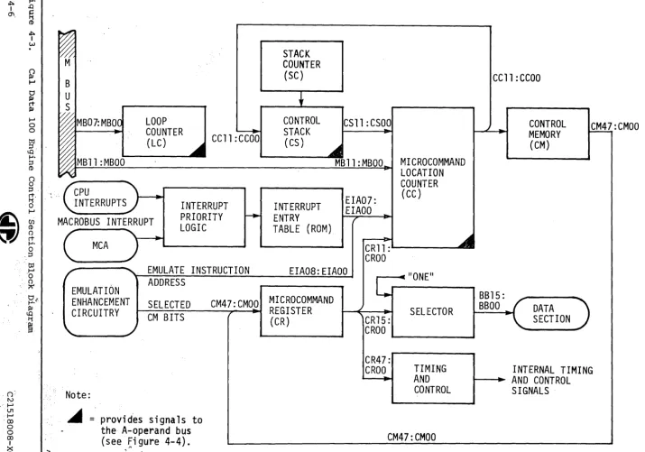
CONTROL SECTION
A block diagram of the control section is shown in Figure 4-3. Control is organized around the control memory (CM), which stores the micro-programs to be executed. Microcommands are 48 bits in length. Normal CM'capacity is from 256 to 4,096 words (48 bits each).
A 12-bit location counter (CC) addresses CM and advances on each clock step unless altered by a sequenc~ cha._nge. Microconunands read from CM are held in a microcommand register (CR) during execution. The micro-commands read from CM can be .. m0dified prior to input to CR for execu-tion. Microcommands can also be entered manually into CR and executed from the Microconsole (not shown).
A 16-level control stack (CS) is provided to permit the contents of CC to be saved and restored under microprogram control. This permits automatic nesting of microroutines and microprogram interrupts, giving increased speed and ~~ space efficiency. Th~-- --~ys_tem contains a unique
f~~~!3-.tY __ tha1: _permit~ def:>ign~ted are~s of_CM_to. .. l.?~.-"Pc;t_c;l}_~g_'~--~~QI.Il_
~~=-ilia~CM .. or __ from ____ tlle ___ ~-~~C?~~~sole •. This is a highly useful feature, since nonalterable storage elements are generally used to implement CM. An eight-bit loop counter (LC) is provided to permit single microcom-mands or entire sequences to be repeated a specified number of times. This feature enhances execution speed of iterative loops.
A special feature of the Cal Data 100 Engine is emulation enhancement circuitry, located on a separate Emulate Board. This circuitry provides:
a. Automatic table-generated addresses :to CC to steer the micro-program directly to specific emulation microroutines, by-passing
lengthy processing to decode instruction codes and addressing modes
b. Automatic interrupt microroutine location entry to CC
c. Automatic table-generated modifiers to microcommands read from · CM
d. Automatic modification of processor status conditions for the emulated instruction
e. Direct designation of word or byte-mode operations
Emulation-related features are described in a separ.ate emulation user manual, available for each computer m~del.
4.2.1 Control Memory (CM)
C21518008-X0°
The control memory is a high-speed, random-access unit. Three device implementations can be used:
a. Read-only memory (ROM). These bipolar semiconductor devices are organized on chips of four by 256 (or f~ur by 512) bit·5·: .. ; Twelve such devices implement each 256-word (or 512-~ord) CM~ page. The code pattern in each chip is permanently inscribea during the factory manufacturing process and cannot b'e altered.
~
I
°'
~
< ( ) ' ' tv
, . . . I-"
. l11
... . 00 0 0 00 I x 0 ~ ...
'°
s=t; Cl) ~ I w
.
() p.i ... 0 p.i rt p.i ... 0 0 l:Ij !:1,t.Q ...
!:1 Cl) () 0 !:1 rt. t; 0 ... c:n Cl) () rt ... 0 . !:1 tJj ... 0 ()
.· 7;"'
~
...
p.i t.Q t; ·~ M Bu
s
LOOP
COUNTER
(LC)
CCll :CCOO
MACROBUS INTERRUPT
INTERRUPT
PRIORITY
LOGIC
MCA
STACK
COUNTER
(SC)
CONTROL
STACK
(CS)
INTERRUPT
ENTRY
TABLE (ROM)
CSll: CSOO
MBll :MBOO
EIA07:
EIAOO
MICROCOMMAND
LOCATION
COUNTER
(CC)
CRll : " - - - -...
CROO
CCll:CCOO
CONTROL
MEMORY
(CM)
CM47:CMOO
EMULATE INSTRUCTION
EIA08: EIAOO
-11
0NE
11EMULATION
ADDRESS
ENHANCEMENT
SELECTED
CM47:CMOO MICROCOMMAND
CIRCUITRY
1---:~~---1~REG I ST ER
CM BITS
(CR)
Note:
~
=provides signals to
the A-operand bus
(see figure
4-4).
SELECTOR
CR15:
CROO
BB15:
BBOO
DATA
SECTION
.._
____
....
CR47:
CROO
TIMING
AND
CONTROL
CM47:CMOO
INTERNAL TIMING
[image:32.799.33.749.57.558.2]b. Programmable read-only memory (PROM). These bipolar semi-conductor devices are organized on chips of four by 256 bits, pin- and speed-compatible with the equivalent ROM. The code pattern in each device is electrically and permanently
in-scribed by a portable programming device. ~M_is_used_fo~
development and_J_ield..debugging .. _of .. firmware and also for low-'Verlline production firmware packages.
c. Alterable Control Memory (ACM). The Cal Data AOvl is a complete, modular control memory that can be installed in the computer in addition to or in place of ROM and PROM devices. It is imple-mented with bipolar random-access memory devices that can be electrically altered (read/write). When installed in the com-puter, ACM can be loaded and read via the MACROBUS using I/O microconnnands. The ACM can then take control of the CPU for execution of ACM firmware at real-time processor speeds. The ACM is most useful for initial and on-line checkout of new firm-ware prior to conversion to ROM or PROM devices.
The normal maximum capacity of CM is 4K words* when ROM or PROM devices are used. Although each microconunand is 48 bits in length, the CM ad-dressing structure of the microcormnand limits direct access to 2K words; however, a paging scheme between 2K-word blocks permits convenient ac-cess anywhere within 4K words.
Auxiliary Control Memory. It is often desirable to alter the contents of CM, either temporarily or permanently. When nonalterable devices are used, the usual requirement is replacement of the existing devices. The Cal Data loq Engine incorporates circuitry that permits either one or two 32-word blocks of auxiliary memory in. the Microconsole to func-tionally replace designated 32-word blocks in CM. This enables
"patching" for corrections, additions or deletions from existing firm-ware, temporary overlay for diagnostic and troubleshooting operations, etc.
4.2.2 Location Counter {CC)
The location counter is a 12-bit binary counter/register that points to the location in CM of the next rnicroconunand to be executed. The micro-program sequence can be altered conditionally or unconditionally as specified by the programmer and the state of the system. A sequence change is made by loading CC from one of the following sources:
a. CR for programme~ branches b. M bus for compu_ted branches c. The current CS,register
d. A vector from the emulation enhancement circuitry e. An interrupt v,ector
CC normally advances sequentially to the· next location through all.4K locations in CM, including the wrap-around transition from 4,095 to O, .. unless the normal sequence is altered.
*Auxiliary ·power. is· 'required above 512 words.
4.2.3
4-8
CC modifiers from CR and the emulation enhancement circuitry are 11 bits long, permitting branches to occur from these sources within only a 2K-word area. The most significant bit of CC is unaltered for such
branches. To branch to a location outside a 2K-word area, the program-mer must execute a microcomrnand that transfers a full 12-bit branch ad-dress via MB. Interrupt vectors are to only the first 256 CM locations
(i.e., the four most-significant
cc
bits are forced to ZERO).Certain conditions cause an automatic reset of CC to location O (a cor-responding microstatus bit is set for each condition) :
a. A catastrophic system error b. A power-up sequence
The contents of CC can be read by microcomrnand via AB. For systems that do not contain an implemented CS, this provides a means of saving a return location in CM. ·
Microcommand Register (CR)
The 48-bit CR stores the current microcommand read from CM for execution. The'microcomrnand from CM can be modified prior to entry into CR by a function specified by the special decode circuitry on the Emulate Boar~.
CR can also be loaded from the Microconsole to permit direct operator control of internal functions. The least-significant 11 bits of CR · modify CC when a branch operation is specified by the microcommand in CR.
Microcornrnand Sequencing and Timing. The basic clock cycle is 165 ns (adjustable) and, ordinarily, a microcommand is read from CM and 'exe-cuted on each cycle. There is a one-clock delay between the time CC addresses a word in CM and the time that the microcomrnand is transferred to CR for execution. For this reason, when the·n~i:-rnal CC counting se-quence is modified, two clock cycles are required to a~cess the micro-cornmand at the branch location and transfer it to CR~ Furthermore, the microcomrnand accessed at the time CC is modified is transferred to CR even though a branch is being made. Whether or not this "extra" micro-comrnand is executed can be specified by the programmer. The following sequence illustrates the operation:
Time
cc
CR OperationT-1 X. (X-1) I
T. X+l
no
Branch to Y specified_'J:'+l y (X1:_1) Microcomrnand at X+l can be executed
T+2 Y+l (Y) Micro command at branch location
In addition to sequence modification, the programmer can specify· that
. t~e succ~edin·g microconunand be skipped. · In this case, the succeeding
microc~~and is· transferred to CR, but execution is inhibited. Th~s
action. is not considered to be a sequence change since CC continues
normal sequential counting. .
The output of CR is decoded to generate the timing and control signals used throughout the computer.
c21~1aooa~xo·
.
4.2.4
4.2.5
Depending on the microcommand, the least-significant 16 bits of CR can be gated via BB into AU. Alternately, a literal "one" value can be'."' placed on BB.
Control Stack (CS)
cs
contains 16 12-bit registers. that are accessed via the four-bit up/ down stack 'counter (SC)·. When a CC "save" is specified bya
micro-command, 'the contents ,of CC are transferred to CS. The contents of CC are always one greater than the location of the microcommand specifying the save •. Likewise, a microcommand can specify a return operation that transfers the contents of the current CS location tocc.
The return microcommand can simultaneously transfer the (incremented) contents ofcc
to thecs
register that contained the return address. Incrementing and decrementing of SC can be specified independently of the save and return functions. CS permits convenient implementation of re-entrant and multi level subroutin.es-at-:the._mi_9rq_:t_~e.l.. Any microcommand branch condition can specify a save operatIOn with an automatic return to the calling sequence using a Return microconnnand.SC co.unts up from zero, modulo 16, and "rolls over" the boundary in either direction. There ~§_)]._<? __ !_~4J.ccition given for a._ stack ove.rflow. It is the pro_g;:aIT1Iller' s .:r;esponsibili ty to maintain the stack within
-l-i1n.t-t:s:-- .. ---·- -·
--~··---··· ...
. The contents of CS (current location) can be read by microcommand; .however, Cp cannot be directly loade4 and SC is not directly accessible
to the microprogram. The contents of CS, therefore, cannot be saved in the event of a power interruptiqn. It is mandatory that provision be made to execute all returns in ·cs within the" time available for power interruption. Since several milliseconds are available, this imposes no practical restriction on the use of the stack~
Loop Counter (LC)
A powerful feature of the Cal Data Engine is the eight-bit LC that per-mits a single microcommand or a group of microcommands to be automati-cally repeated up to 256 times. LC is loaded via MB and can be read with a microcommand. In a repeat sequence, LC can be tested for a zero
'
:, ' ..
or nonzero condition by any microcommand in the sequence.;1 ... with a branch operation executed if the condition is met. LC is decreni~nt~d each time it is tested. Individual microcommands can also be repeated the number of times specified by LC.
4.3 DATA SECTION
:.~21.s1aoaa~xo
A block diagram of the data section is shown in.Figure 4-4. The ~ata section contains the basic arithmetic, logic and busing elements of the Engine required. for manipulation and transfer of da~a throughout .:t;:he computer.
1-:tj
....
~ l-I ...0 ~
~ I' ~
.
() Ill ... t:1 Ill rt Ill ... 0 0 ttj ::sl.Q
....
::s ct> ~ rt Ill Cf) ct> ()
§
rt....
0 ,::s tD ... 0 () X" t:1
...
Ill . l.Q . 11 Illa
M Bu
s
MB15:MBOO
MS
LOGIC
MICROSTATUS
REGISTER
(MS)
MS06:MSOO
.FILE
REGISTERS
(FR)
CONTROL
SECTION
ARITHMETIC/
AU SHIFT
LOGIC UNIT
ELEMENTS
(AU)
AU15:
(SX)
~---AUOO L...-_ _ _ _ __.
BB15:BBOO
MB15:MBOO
M BUS
SHIFT
BITS
SHIFT
REGISTER
(XR)MB15:MBOO
by a shaded triangle in the lower-right corner of
SAMPLE
*These sources are identified on all block
diagrams~each block providing signals to the A-operand bus:
M
B
u
4.3.l
4.3.2
4.3.3
The data section utilizes 16-bit parallel data paths and operational elements. Provision is made for byte-mode operations. The general file-register (FR). structure provides either eight or 16 general-purpose registers directly addressable by each microcommand. The output of any FR can be selected as either the A- or B-operand input to the arithmetic/ logic unit (AU), and the results of the operation are routed via MB to many destinations (including FR) within the Engine.
Dynamic condition codes indicating conditions of the operational results Ce .• g., overflow, n.egative, etc.) are. generated for each microcommand executed. These conditions can be saved as static status bits. Either the static or the current dynamic conditions can be tested by any micro-command.
File Registers (FR)
FRs provide general-purpose storage within the data section. Either eight or 16 FRs (labeled FRO to FRlS) of 16 bits each can be implemented. The FRs permit the following simultaneous operations to be performed:
a. Any two FRs can be specified as the A- and B-operand sources to AU
b. The FR selected as the A-operand source can also be specified as a destination register
c. Any FR can be specified as a destination register for MB
Operand Buses (AB, BB)
Operands are transferred to AU via AB and BB, part of the Microbus. All microcormnands executed by the CPU involve the use of information on one or both of these buses.
AB sources can be selected from any one of the FRs or from one of 11 other operational registers in the computer. There are five unused AB source addresses, of which two are reserved for user-defined functions. The BB source can be:
a. Any one of the FRs
b. The least-significant 16 bits of the current micrqcommand contained in CR
c. A literal "one" value
The second BB source listed above represents a l6-bit literal value con-tained in the microcommand.
Arithmetic/Logic Unit (AU)
AU is a 16-bit parallel element that performs arithme,tic (Appendix A) and logical functions on two variables inp~t via AB ·and' BB with the link
(L) status bit from the microstatus register (MS) used conditionally as a carry input for addition and subtraction operations. A carry output
(c) , resulting from AU operations, can be tested as conditional skip or branch condition and can also be stored in MS (in the L bit) as a static . status condition·.
4.3.4
4.3.5
4.3.6
Each microcommand specifies, either implicitly or explicitly, the AU
operation to be performed and the use of the L input. A total of 15 logical and eight arithmetic functions are implemented.
AU Shift Elements (SX) and Shift Register (XR)
SX is a set of gates that can be used in conjunction with shift register XR for shifting an AU operand. The following can be performed:
a. Left shift one bit
b. ~ght shift one bit (l.ogi.cal or arithmetic) c. swap more-s.igni.ficant and less-s.ignificant bytes
d. Swap more-s.ignificant and less-s_ignificant halves of the less-s_ignif icant byte
For shift operations, the L bit in MS is normally used as the shift carry-in and c is the bit shifted out of SX. This carry bit can be saved as L for the next AU operation.
Provision is made for both single- and double-length shifts, either of which can be logically open, closed or arithmetic. Double-le_ngth shifts are performed in conjection with XR, which is a 16-bit shift register. In this case, the L input and c output are dependent on.the direction of the shift. For left shifts, sx holds the more-significant 16-bit word. For right shifts, XR holds the more-significant word.
Shifts are performed by using shift operation codes in microcommands. Because the A operand is always used in the.shift, AU performs a "copy" AB operation. Shift microconunands must specify the type of shift to be performed and the carry input function.
Multibit shifts can be performed by the use of LC by setting up a shift count and repeating the microcommand. This permits execution of shifts of all types to be performed in one clock step per bit shifted.
M Bus (MB)
MB., .a part of the Microbus, receives the resultant output from an AU or shift operation and provides the transfer path to all internal computer destinations. Each microcommand specifies a destination address to one MB location. In addition, by setting one bit of the microcommand, the
AU result· · C'a~ be tr an sf erred to the AB source. Microcondition Codes
For·each operation performed by .the AU or shift gates, a set of condition codes .is.dynamically generated, describing the result. These are:
a..' ··::carry-d~t:;;:.(c). The carry-out is generated a~ the arithmetic carry fqr.an add operation, the borrow for a subtract operation '.or .the shift carry-out for a shift operation. .·. ' b. OV~rflow (v) • . Overflow is generated for add, subtract or: .shift
operat~ohs •. · The conditions under which overflow oc,curs ,::·depends on the
4.3.7
c. Zero (z). The zero condition exists when all bits of the result are ZERO.
d. Negative (n). The negative condition exists when the most-significant bit of the result (shifted, if applicable) is ONE. e. Positive (p). The positive condition exists when the result
is· greater than zero (not zero and not negative).
f. Odd (d). The odd condition exists when the least-significant bit of the result is ONE.
The last four conditions are referred to as data value codes and are generated from the value of the AU result on MB.
A microcommand can specify dynamic conditional testing of the micro-condition codes generated as the result of an operation, and the condi-tional test can cause a skip of the next microconnnand or a branch to a new microprogram location. This capability saves considerable time over machine designs that require conditional testing to be performed on the condition generated by a previous operation.
Microstatus Register '(MS)
The six dynamic condition codes can be saved as static microstatus bits in MS. Each microcommand can specify separate storing of the carry/ overflow and the four data value codes in MS. These static microstatus conditions (instead of the dynamic microcondition codes) can.then be ·tested by microcommands for conditional skips or branches.
MS is 16 bits in length. In addition to the six microcondition codes, other status bit~ are stored in this.register. The contents of MS can be read via AB and can be loaded as a destination via MB. The complete set of status bits contained in MS is defined in Table 4-1.
Table 4~1. Microstatus Register Bit Definitions
MS Bit Symbol Name Description
00 L Link Stored state of dynamic
carry-out (c) of AU or shift gates 01
v
Overflow Stored state of dynamicarith-me tic or ... s~;i.J;t overf iow (v)
: ;·'t·,. ',\.,.1-.
'•
02
z
Zero Stored state of zero (z) datavalue code
03 N Negative Stored s~ate of negative (n) data ·'.value co,t.1~ .
. .. ~~ r.~ .
.,.
04 p Positive store~ state o~ positive (p)
; ,
data vc;tlue· code
' ' ( .. \
..
05 D Odd
..
Stored:» state of odd (d) data value · 'C'ode15 to~06 Special use, depending on . "
... ,.
emulation
. . . .
.
: _.·r· ,. L. .I ,, ,._,,'
• ~ 4
..
..
. '
[image:39.615.50.575.32.792.2]