Please cite this article as: M. Javadi, H. Miar-Naimi, S. M. Hosseini-Andargoli, A ModifiedNoise Analysis of a Common Source ̶ Common Gate Low Noise Transconductance Amplifier for Sub-micron Technologies, International Journal of Engineering (IJE), IJE TRANSACTIONS B: Applications Vol. 31, No. 11, (November 2018) 1903-1909
International Journal of Engineering
J o u r n a l H o m e p a g e : w w w . i j e . i rA Modified Noise Analysis of a Common Source
̶ Common Gate Low Noise
Transconductance Amplifier for Sub-micron Technologies
M. Javadi*, H. Miar-Naimi, S. M. Hosseini-Andargoli
Department of Electronics, School of Electrical and Computer Engineering, Noshirvani University of Technology, Babol, Mazandaran, Iran
P A P E R I N F O
Paper history: Received 04 March 2018
Received in revised form 31 October 2018 Accepted 06 November 2018
Keywords:
Low Noise Amplifier (LNA)
Low Noise Trans-conductance Amplifier (LNTA) Noise canceling LNTA
Surface Acoustic Wave -less receiver Wideband receiver
A B S T R A C T
This paper is based on analysis of a common source - common gate low noise transconductance amplifier (CS-CG LNTA). Conventional noise analyses equations are modified by considering to the low output impedance of the sub-micron transistors and also, parasitic gate-source capacitance. The calculated equations are more accurate than calculated equations in other works. Also, analyses show that the noise of the tail transistor, which is utilized to bias the common gate transistor, will limit noise canceling advantages. So, the common gate transistor is biased by a resistor. That leads to a significant improvement in noise figure. By utilizing a Taylor series expression, a closed-form equation is obtained to calculate IIA3 for the first time. Finally, based on the calculated equation a design procedure is proposed.
doi: 10.5829/ije.2018.31.11b. 14
NOMENCLATURE
Rocs Output resistance of the CS stage Cgscs parasitic gate-source capacitor of the CS transistor
Rocg Output resistance of the CG stage α Voltage divider factor between Cbcs & Cgscs
Rmixer Input resistance of the mixer Cbcs coupling capacitor
Rcs Equvalent gain of mixer & TIA in CS path rob Output resistanc of the tail transistor
Rcg Equivalent gain of mixer & TIA in CG path Rs Antenna resistance
gmcg Transconductance of the CG stage F Noise factor
gmcs Transconductance of the CS stage
1. INTRODUCTION1
Commercial advantages of multi-standard devices play a crucial role in the growth of the modern receivers in recent years. Multi-standard receivers must be high linear, low noise figure (NF), and low power consumption to obtain the best performance [1]. The current-mode receiver is more linear than the voltage mode counterpart, mainly due to having lower voltage gain and one-time use of the nonlinear voltage to current conversion. Another important feature of the multi-standard receivers is the ability to work in several frequency bands. Surface Acoustic Wave (SAW) filters,
*Corresponding Author Email: [email protected] (M. Javadi))
which pass signals only on a special frequency band, are not utilized in highly integrated multi-standard applications [2-6].
approach results in a linear receiver, NF increases due to the absence of the LNA [2]. Utilizing a low noise transconductance amplifier (LNTA) is another structure for a SAW-less receiver to drive CDPM and reduce the noise effect of the next blocks including the mixer and Trans-Impedance amplifier (TIA). This approach improves NF in comparison with mixer-first topology while degrades the overall linearity of the receiver [4].
Although there is usually a trade-off between NF and linearity, there are noise and nonlinearity cancellation techniques that improve both parameters, concurrently. In these approaches, noise and nonlinearity of the main path are approximately canceled out by an auxiliary path [9]. CS-CG LNA is one of the popular structure which utilizes this technique. In the structure, the noise of the main path (CG path) is canceled out by auxiliary path (CS path).
The reduction of the output resistor in transistors, which is cuased by the ongoing scaling of semiconductor technologies, introduces new challenges for the design of a current-mode analog circuit.
In this work, the effect of the low output resistor of the transistors on linearity and NF are investigated for a CS- CG LNTA. We have obtained the closed form equations to compute the noise factor and IIP3. The noise factor of the CS-CG LNA is obtained but the noise of the tail transistor and also the output impedance of the transistors is ignored [10]. In this work, the effect of the low output resistor of the transistors on linearity and NF are investigated for the CS-CG LNTA. Besides, we present a closed-form equation to calculate the IIP3 for the CS-CG LNTA for the first time that also can be utilized for CS-CG LNA.
The rest of the paper is as follows. NF of The conventional CS-CG LNTA with two kinds of biasing methods are studied in section II and section III. The linearity of the CS-CG LNTA is calculated in section IV. In section V, the design procedure is proposed.
2. NOISE ANALYSIS OF A CURRENT SOURCE BIASING CS-CG LNTA
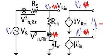
The main idea of the noise canceling is introduced in Figure 1. There are two paths to cancel out the noise of the matching resistor. In one path, the matching resistor current is measured and is amplified by β, and in another path. The voltage of the matching resistor is measured and is gained by δ. In an ideal situation, there is a ratio of β/δ that the noise of the matching resistor can be completely canceled out at differential output. Figure 2 shows a current mode implementation of a noise canceling receiver. In the Figure, gm,main and gm,aux
are transconductance of the CG and CS transistor,
respectively. In current mode topology,
noise/nonlinearity of the main path transistors is usually
canceled out by recombining signals of two paths. A simplified circuit of this technique in current mode is shown in Figure 3.
The common gate configuration, implemented by Mcg, is utilized as an active matching circuit while that
also measures the current in the input resistance as well. Mcs has a common source structure to amplify the
voltage of the active input resistance (input seen impedance from the gate of the Mcg). To simplification,
mixer and TIA are modeled as a trans-impedance amplifier.
Figure 1.Conceptual circuit of the noise canceling method
Figure 2. Current-mode noise/nonlinearity cancellation
receiver
In this figure, 2 , n cg
I , 2
, n cs
I and In b2, are noise of the Mcg, Mcs and Mb, respectively. The differential output noise is computed as follows:
2 , 2 2 , 2 2 2 , , 2 2 , = 1 2 2 2 2mcg S ocg
n out cg
ocg mixer
mcs S ocs
cs n cg ocs mixer
mcg S ocg cg ocg mixer
mcs S ocs
cs n b n Rs ocs mixer
ocs
cs n cs ocs mixer
g R R
V R
R R
g R R
R I
R R
g R R
R
R R
g R R
R I I
R R R R I R R (1)
where 2 , n Rs
I represents the noise of the antenna resistor
(Rs) gmcs, and gmcg are trans-conductance of the CS transistor and the CG transistor, respectively. Rocg and Rocsdemonstrate the output impedance of the CG and CS stage, respectively. Rmixeris input impedance of the Mixer. The channel Noise of the M1 and M2 have a
negligible impact on the total noise factor. So, the effect of them is ignored on the noise factor calculations. α is voltage divider factor between coupling capacitor (Cbcs) and parasitic gate-source capacitor of the CS transistor (Cgscs) that is obtained from Equation (2).
= bcs bcs gscs C C C (2)
The ratio of the baseband gain of the main path per baseband gain of the auxiliary path should be set as Equation (3) to cancel out the noise of the CG transistor.
= = 2 2 ocs mcs scg ocs mixer cs mcs s ocg
cs mcg s cg
mcg s
ocg mixer R g R
R R R g R
R
R g R
g R R R (3)
Suppose that output impedance of the bias transistor is rob. Thus, gmcg should be chosen Rs-1− 2rob-1 to satisfy matching condition. Therefore, we can calculate noise factor as:
22 2 2 2 = 1 2 1 2
= 1 1
mcg s mb s mcs s s ob s
ob mcs s g R
F g R
g R
R r R
r g R
(4)
According to (4), the low output impedance of the bias transistor increases the noise factor. In the derived expression, noise factor of the conventional noise/nonlinearity ca ncellation can be decreased by increasing gmcs but the minimum achievable noise factor of this structure is limited to 1+γ. The second term of (4) is caused by the Mb. Noise of the tail transistor, low output impedance of the transistors and also voltage divider factor (α) is ignored in [11] while these can have
a significant effect on the total noise factor. In [12], without considering to the noise of the load resistance of the LNA, the noise factor after simplification is obtained as: = 1 mcs s F g R (5)
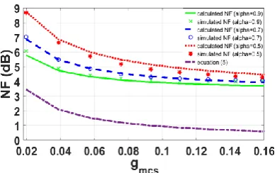
Please notice that the computed noise factor in literature [13] is for an LNA. We ignore the noise of the load resistances in Equation (5) to have a fair comparison. Simulated noise contribution of the transistors in current-biasing CS-CG LNTA (Figure 4) is introduced in Figure 5. All of the simulations are done in cadence. The noise of CS transistors (Mncsand Mpcs) goes down by increasing gmcswhile the noise of the other elements is constant approximately. The noise of M1, M2, Mpcg, and Mncg are negligible. For a high value of gmcs, the noise of tail, transistors play a major role in the overall noise factor. Figure 6 shows the NF of the current-biasing CS-CG LNTA versus gmcs for various α. By increasing gmcs, the NF is improved but it is limited because of the noise of the current biasing transistor (Mb). An inductor can be utilized instead of Mb to provide bias path for Mcg. However, this topology occupies a large area. Therefore, a resistor can be utilized to bias the CG transistor instead of the use of an inductor for very large scale integrated receivers.
Figure 4. Conventional CS-CG LNTA by current biasing
Figure 6. NF of current-biasing CS-CG LNTA versus gmcs for various α
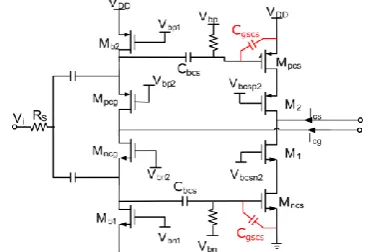
3. NOISE ANALYSES OF A RESISTOR-BIASING CS-CG LNTA
A complementary structure for RF transconductance stages is usually utilized to save area and power consumption. A wide CG transistor or a low bias resistor can be used to satisfy matching condition. The first degrades the maximum operating frequency and mistunes the noise canceling of the CG transistors because of parasitic capacitances. The second increases power consumption in comparison with the first way and also increases noise factor because a lower gmcg will be needed for CG transistor to match the input impedance of the LNTA. On the other hand, the input impedance of the LNTA is gmcgp + gmcgn + (2/Rb). So, by decreasing Rb, the value of the overall gmcg(gmcgp + gmcgn) should be reduced to satisfy the exact matching condition. The noise factor of this structure can be calculated by Equation (6).
22
2
2 2 2
= 1
2 1 2
= 1
mcg s s
b mcs s
s b s
b mcs s
g R R
F
R g R
R R R
R g R
(6)
The low value of the Rb increases noise factor directly (second term of Equation (6)) and indirectly (third term of (6)). The second term of Equation (6) goes up by reducing Rb. Low value of the Rb leads the gmcgRs to lower value than one. So, the third term of Equation (6) is increased by lower Rbtoo. However, the LNTA by a CG transistor which is biased by a resistor (Figure 7) has a lower noise figure than the LNTA by a current– biasing CG transistor.
Figure 8 presents the noise contribution of the elements in Figure 7. Unlike the current-biasing CS-CG LNTA, CS transistors play a major role in total noise factor. Noise contribution of the CS transistors goes down by increasing gmcs. Figure 9 shows NF of resistor-biasing CS-CG LNTA for various α. Same as the current-biasing CS-CG LNTA, the NF of the resistor-biasing CS-CG LNTA goes up by decreasing α.
Figure 7. Conventional CG-CS LNTA by resistor biasing
Figure 8. Noise contribution of transistors in resistor-biasing CS-CG LNTA versus gmcs (α=0.9)
Figure 9. NF of resistor-biasing CS-CG LNTA versus gmcs for
various α
4.LINEARITYANALYSIS
A Taylor series expression is utilized to calculate the lin- earity of the LNTA (see Appendix). By considering to low voltage gain for the LNTA, nonlinear transconductance (gm) of the transistors plays a major role in overall nonlinearity. The output voltage of the noise/nonlinearity cancellation receiver (Figure 3) can be illustrated as follows:
2 3
1 2 3
=
out s s s
V H V H V H V (7)
1
1 1
=
2 mcg cg cg 2 mcs cs cs
H g R g R (8)
' '3
2
' 2 '
2 '
' '
= 2
16 16
[
16 16 16
2
] 16
S mcg mcg cg cg mcg s
mcs S mcg mcs S mcg mcs
cs cs
S mcs mcg
R g g
H R g R
g R g g R g
g R
R g g
(9)
Using Equation (3), receiver gain (H1) and IIA3 can be calculated by Equations (10) and (11), respectively.
1=
cg cg
S R H
R
(10)
2
' ' '
2 3
3 = 1
32
s mcs S b
mcs S mcg mcs
R IIA
g R R
g R g g
(11)
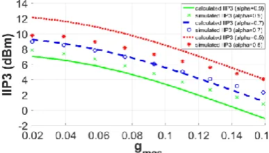
Regarding utilize a complementary structure for CS and CG transconductance stage; the second order nonlinearity has a very low value in comparison with the third-order nonlinearity. So, the second term of the nonlinearity can be ignored for the designed transconductore stage. Also, decreasing α can help to improve linearity, but it goes up the NF. IIP3 of the current- biasing and resistor-biasing LNTA versus gmcs for various α is plotted in Figures 10 and 11, respectively.
Figure 10. IIP3 of current-biasing CS-CG LNTA versus gmcs for various α
Figure 11. IIP3 of resistor-biasing CS-CG LNTA versus gmcs
for various α
5.DESIGNPROCEDUREOFTHECS-CGLNTA
To design of a CS-CG LNTA, a 20 mS transconductance stage (we call it to reference transconductance stage) should be designed at first. Then, some parameters of the gm transconductor including the output resistance (Ror), gate-source
capacitance of the Mncs and Mpcs (Cgsr), and output
resistance of the Mncs or Mpcs (rob) should be calculated
by simulation. The width of the transistors can be set N times of the width of the transistors of the reference transconductance stage to achieve the desired gm stage (N20mS) for CS stage. Moreover, the first-order and second-order non- linearity can be plotted versus gm (Figure 12). The plotted curves can write as a function of gm. Next, using Equation (6) (or Equation (4) for current-biasing version) and Equation (11), we can plot the NF and IIP3 by varying gmcs and α same as Figures 13 and 14.
Figure 12. First-order and second-order transconductance
nonlinearity of the CS stage versus gmcs
Figure 13. Estimated NF of resistor-biasing CS-CG LNTA
versus gmcs and α
Figure 14. Estimated IIP3 of resistor-biasing CS-CG LNTA
After choosing the gmcs and α from these figures to have
the desired NF and IIP3, we can obtain other values for the elements that is utilized in the receiver.
Cgs of the designed CS stage is N×Cgsr while the Rocs
is Ror/N. By these values and a reasonable value for
Rmixer, we can calculate αcg and αcs. Besides, Cbcs can be
calculated by Equation (2). For the desired value for a voltage gain of the receiver, Rcg can be computed from
Equation (10). Rcg demonstrates the equivalent gain of
the mixer and the TIA in the main path. So, the R1
(feedback resistor of the TIA in the main path (Figure 2)) is calculated as:
1
2 cg
R R (12)
Also, Rcs can be computed by Equation (3). So, the R2 is
2Rcs
.
6.CONCLUSION
The low output impedance of the transistors in CS-CG LNTA is considered and new situation to cancel out the noise of the CG transistor is obtained. Analyses show that the noise of the current source transistor limits the NF in current-biasing CS-CG LNTA. So, it is better to use a resistor instead of the current source transistor to bias the CG transistor. Using the small biasing resistor increase the NF while high biasing resistor limits the operational frequency. For the first time, a closed-form equation is obtained to calculate the IIP3 of the CS-CG LNTA. Totally a design procedure to design the CS-CG LNTA is illustrated.
7. REFERENCES
1. Liscidini, A., “Fundamentals of Modern RF Wireless Receivers: A Short Tutorial”, IEEE Solid-State Circuits Magazine, Vol. 7, No. 2, (2015), 39–48.
2. Murphy, D., Darabi, H., Abidi, A., Hafez, A A., Mirzaei, A., Mikhemar, M., Chang, M.C.F., “A Blocker-Tolerant, Noise-Cancelling Receiver Suitable for Wideband Wireless Applications”, IEEE Journal of Solid-State Circuits, Vol. 47, No. 12, (2012), 2943–2963.
3. Ud Din, I., Wernehag, J., Andersson, S., Mattisson, S., and Sjoland, H., “Wideband SAW-Less Receiver Front-End With Harmonic Rejection Mixer in 65-nm CMOS”, IEEE
Transactions on Circuits and Systems II: Express Briefs, Vol.
60, No. 5, (2013), 242–246.
4. Fabiano, I., Sosio, M., Liscidini, A., and Castello, R., “SAW-Less Analog Front-End Receivers for TDD and FDD”, IEEE
Journal of Solid-State Circuits, Vol. 48, No. 12, (2013), 3067–
3079.
5. Ud Din, I., Wernehag, J., Andersson, S., Sjöland, H., and Mattisson, S., “Tunable wideband SAW-less receiver front-end in 65 nm CMOS”, Analog Integrated Circuits and Signal
Processing, Vol. 77, No. 1, (2013), 3–16.
6. Kim, J., and Silva-Martinez, J., “Low-Power, Low-Cost CMOS Direct-Conversion Receiver Front-End for Multistandard Applications”, IEEE Journal of Solid-State Circuits, Vol. 48, No. 9, (2013), 2090–2103.
7. Mohamed, S.A.S., and Manoli, Y., “Design of Low-Power Direct-Conversion RF Front-End With a Double Balanced Current-Driven Subharmonic Mixer in 0.13 µm CMOS”, IEEE
Transactions on Circuits and Systems I: Regular Papers, Vol.
60, No. 5, (2013), 1322–1330.
8. Wu, C., Wang, Y., Nikolic, B., and Hull, C., “An Interference-Resilient Wideband Mixer-First Receiver With LO Leakage Suppression and I/Q Correlated Orthogonal Calibration”, IEEE
Transactions on Microwave Theory and Techniques, Vol. 64,
No. 4, (2016), 1088–1101.
9. Blaakmeer, S.C., Klumperink, E.A.M., Leenaerts, D.M.W., and Nauta, B., “Wideband Balun-LNA With Simultaneous Output Balancing, Noise-Canceling and Distortion-Canceling”, IEEE
Journal of Solid-State Circuits, Vol. 43, No. 6, (2008), 1341–
1350.
10. Javadi, M., Sheikhaei, S., and Kashi, A.S., “Design of a direct conversion ultra low power ZigBee receiver RF front-end for wireless sensor networks”, Microelectronics Journal, Vol. 44, No. 4, (2013), 347–353.
11. Masoumi, N., and Aghnout, S., “Modeling of Substrate Noise Impact on a Single-Ended Cascode LNA in a Lightly Doped Substrate (RESEARCH NOTE)”, International Journal of
Engineering - Transactions A: Basics, Vol. 23, No. 1, (2010),
23–28.
12. Sedaghat, S.B., Karimi, G., and Banitalebi, R., “A Low Voltage Full-band Folded Cascoded UWB LNA with Feedback Topology”, International Journal of Engineering -
Transactions A: Basics, Vol. 28, No. 1, (2015), 66–73.
13. Asemani, M., Ardeshir, G., and Razmjooei, D., “Improving Linearity of CMOS Variable-gain Amplifier Using Third-order Intermodulation Cancellation Mechanism and Intermodulation Distortion Sinking Techniques”, International Journal of
Engineering - Transactions B: Applications, Vol. 30, No. 2,
(2017), 192–198.
8.APPENDIX:TAYLOR SERIES ANALYSIS
Tylor expansion of the Ics and Icgand Viare defined in (A.1)-(A.3), respectively. Icsand Icgare output current of the CS and CG transconductance stage. Viis the input voltage of the LNTA.
2 3
1 2 3
=
cs s s s
I AV A V A V (A.1)
2 3
1 2 3
=
cg s s s
I B V B V B V (A.2)
2 3
1 2 3
=
i s s s
V D V D V D V (A.3)
on the other hand, the Icsand Icg can be introduced by (A.4) and (A.5), respectively.
2 ' 2 3 ' 3
=
cs mcs i mcs i mcs i
I g V g V g V (A.4)
' 2 ' 3
=
cg mcg i mcg i mcg i
I g Vg V g V (A.5)
1= mcs 1
A g D (A.6)
2 ' 2 2= mcs 2 mcs 1
A g D g D (A.7)
2 ' 3 ' 3
3= mcs 3 2 mcs 1 2 mcs 1
A g D g D D g D (A.8)
Taylor series coefficients of the Icg are as follows:
1= mcg 1
B g D (A.9)
' 2 2= mcg 2 mcg 1
B g D g D (A.10)
' ' 3
3= mcg 3 2 mcg 1 2 mcg 1
B g D g D D g D (A.11)
By a node analysis at the input node, (A.12) can be obtained.
= i s i
cg
s ob
V V V
I
R r
(A.12)
The coefficients of the Vi is determined by (A.13)-(A.15).
1 1 1
1
= = 0.5
s s ob mcg
D
R Rr g (A.13)
' 2=
8
s mcg
R
D g (A.14)
2 2
' '
3=
8 8
s s
mcg mcg
R R
D g g (A.15)
By calculating D1–D3, other variable coefficients can be
calculated such as A1-A3 and B1-B3. Finally, Taylor
coefficients of the Vout can be calculated by using (A.16).
=
out cg cg cg cs cs cs
V R I R I (16)
A Modified Noise Analysis of a Common Source
̶ Common Gate Low Noise
Transconductance Amplifier for Sub-micron Technologies
M. Javadi, H. Miar-Naimi, S. M. Hosseini-Andargoli
Department of Electronics, School of Electrical and Computer Engineering, Noshirvani University of Technology, Babol, Mazandaran, Iran
P A P E R I N F O
Paper history: Received 04 March 2018
Received in revised form 31 October 2018 Accepted 06 November 2018
Keywords:
Low Noise Amplifier (LNA)
Low Noise Trans-conductance Amplifier (LNTA) Noise canceling LNTA
Surface Acoustic Wave -less receiver Wideband receiver
کچ هدی
تیوقت کی هلاقم نیا رد یم هدافتسا یگنیطخان و زیون فذح کینکت زا هک زیون مک یاناسرارت هدننک
دنک دروم ارق یسررب ر
یجورخ سنادپما نتفرگ رظن رد هب هجوت اب لوادتم طباور .تسا هتفرگ گ و سروس نیب کیتزاراپ نزاخ و
تی
م ریز یاهروتسیزنارت هدش حلاصا نورکی
ک ریاس رد هدش تابثا رگید طباور زا هدش هبساحم طباور .دنا د اهرا
قیق و رت هداس رت
دنتسه یم ناشن اهزیلانآ نینچمه . سایاب روتسیزنارت زیون هک دنهد
وف ،کرتشم تیگ روتسیزنارت هدننک کت دیا
ون فذح کین زی
یم دودحم ار کی اب کرتشم تیگ روتسیزنارت نیاربانب .دنک
بهب ببس راک نیا .تسا هدش سایاب تمواقم نعم دو
رد یرادا
تسا هدش هدافتسا رولیت یرس زا یناسطخ هبساحم یارب نینچمه .تسا هدش زیون نازیم
.
ب هلاقم نیا رد راب نیلوا یار
هطبار و هدش لیلحت راتخاس نیا یگنیطخ رس .تسا هدیدرگ هئارا هتسب یا
اجنا تابساحم یانبم رب ماجنا هدش م
ی ، هیور ک
.تسا هدش داهنشیپ ناحارط یارب یحارط