Please cite this article as: M. Katebi, A. Nasri, S. Toofan, H. Zolfkhani, A Temperature Compensation Voltage Controlled Oscillator Using a Complementary to Absolute Temperature Voltage Reference, International Journal of Engineering (IJE), IJE TRANSACTIONS B: Applications Vol. 32, No. 5, (May 2019) 710-719
International Journal of Engineering
J o u r n a l H o m e p a g e : w w w . i j e . i rA Temperature Compensation Voltage Controlled Oscillator Using a Complementary
to Absolute Temperature Voltage Reference
M. Katebi*, A. Nasri, S. Toofan, H. Zolfkhani
Integrated Circuits Laboratory, Electrical Engineering department, University of Zanjan, Zanjan, Iran
P A P E R I N F O
Paper history:
Received 12 September 2018
Received in revised form 05 March 2019 Accepted 03 May 2019
Keywords:
Colpitts
Complementary to Absolute Temperature Cross-coupled Pair
Temperature Compensation Voltage Controlled Oscillator
A B S T R A C T
T his paper presents a temperature compensation voltage controlled oscillator (VCO) based on Cross-Coupled pair and Colpitts structures which is suitable for military fields. Also, two inductors have been used for increasing the negative conductance. By using this method, start -up condition has been improved. Two varactors and a simple capacitor bank are applied for covering a wide tunning range. T he VCO has been designed and simulated in T SMC 0.18 µm CMOS technology.To compensate the frequency drift over a temperature range, MOS varactors are used and biased with a complementary to absolute temperature (CTAT) voltage reference. This CT AT voltage reference has been applied to two varactors and decreased the frequncy drift over temperature range. By using this technique, the proposed VCO can achieve a very stable frequency o f 11.5 PPM/°C at 24.35 GHz over a temperature range of -40~120 °C. Simulation results also show the VCO covers the frequency range of 23.75~24.8 GHz. T he simulated phase noise of center frequency is -102.6 dBc/Hz at 1 MHz offset frequency. T he VCO consumes 10.4 mW DC power under 1.8 V supply voltage. The figure of merit of the VCO is -179.8 after compensating.
doi: 10.5829/ije.2019.32.05b.13
1. INTRODUCTION1
Frequency drift over temperature variations is a crucial design consideration for voltage controlled oscillator (VCO) circuits in RF systems because transistors’ parameters, on-chip inductor resistances, and capacitors are highly sensitive to temperature fluctuations [1]. Temperature compensation for the VCO oscillation frequency is a critical issue for RF designer. Also, it is important to improve other parameters of VCO like power consumption and phase noise after frequency compensating over the temprature range. The phase noise and power consumption are two critical issues in designing VCO [2]-[5].
Several methods are proposed to compensate frequency drift over temperature [6]-[11]. Placing VCO in a synthesizer loop is a solution for this problem [12]. The correcting nature of the synthesizer can decrease the frequency drift of VCO, in closed loop condition,
*Corresponding Author's Email: [email protected] (M. Katebi)
to fix the frequency drift. This Reference has used BiCMOS Technology. Therefore, the cost has increased. By employing a complementary to absolute temperature (CTAT) voltage reference in [8], the frequency drift has been compensated. To design the CTAT voltage, an opamp has been used to fix the voltage deviation and then the output of the opamp has been connected to a MOS transistor for producing the CTAT current. This current has been passed through a resistor to produce a CTAT voltage. This circuit could have compensated the frequncy drift but it suffers from poor phase noise performance.
A temperature compensation technique using constant-biased varactors has been presented in reference [9]. In this circuit to compensate the frequncy drift, PMOS varactors have been used. According to this reference, PMOS varactors have better characteristics than NMOS varactors. This circuit has a good performance but the frequency of the circuit is low. Reference [10] has presented an LC cross -coupled VCO. To design this VCO, T-lines have been used instead of inductors and the size of circuit has decreased. But the circuit suffers from high power consumption and poor phase noise.
Most designs in the field of VCO temperature compensation have been performed at frequencies less than 10 GHz. Therefore, it is extremely important to design a VCO at high frequencies with temperature compensation. The other important issue in designing a VCO is the structure of its circuit. Cross -Coupled pair and Colpitts VCOs are the two mostly used structures due to their good performance like phase noise and dc power consumption at high frequencies. Therefore, , it is important to design a high frequncy VCO with good phase noise and low power consumption. Also, it is critical to have a stable frequency and performance over a wide temperature range.
In this paper, a temperature compensation VCO with good noise performance at 24.35 GHz is presented. To achieve good temperature performance, a CTAT voltage reference is applied to varactors. This helps the circuit to be stable over a wide temperature range and it fixes the frequency changes with a good approximation. By using this compensation circuit, the resulting drift from center frequency is 11.5 PPM/C. Besides, to achieve good performance, combination of Cross -Coupled pair and Colpitts structures are used. This circuit is suitable for military fields. Because it is stable over a wide temperature range.
The rest of the paper is organized as follows: the proposed VCO and temperature drift reasons are introduced in Section 2. The temperature compensation circuit is presented in Section 3. Design considration is proposed in Section 4. Section 5 discusses simulation results and compares it with the results of prior works. Finally, conclusion is provided in Section 6.
2. THE MAIN PART OF VCO AND FREQUENCY
DRIFT CONSIDERATION
2. 1. VCO Core The schematic circuit of proposed
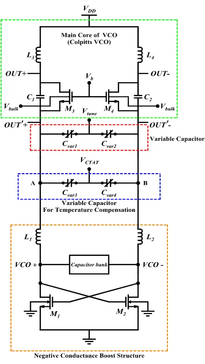
VCO has been shown in Figure 1. The proposed VCO includes Cross-Coupled pair and Colpitts structures. The Cross-Coupled pair is used due to its better start-up condition and low phase nois e performance [13]. Also, by using Colpitts structure, DC power consumption has been reduced [13]. To have a better start-up condition, two inductors have been used between Cross -Coupled pair and Colpitts structures [14]. These inductors enhance the interesting gain of transistors and thus, the negative conductance increases leading to robust start -up condition. Moreover, these inductors reduce the noise effect of Cross-Coupled pair by resonating with parasitic capacitors of the trans istor at oscillation frequency. Therefore, phase noise performance is improved. In addition, a simple capacitor bank and two varactors have been applied to have an acceptable tuning range.
To improve the start-up condition, a voltage is applied to bulk of transistors M3-4. To prove this claim, the transconductance gain is obtained as
GS o SB
m th
ω
= μ Cn o V - V - γ( V -2 - -2 ) L
g x (1)
where, µn, Cox, 𝜔
𝐿, VGS, VSB, Vtho, and are mobility of electrons, silicon dioxide capacitor, size of transistor, gate-source voltage, bulk-source voltage, threshold voltage (VSB=0), bulk threshold parameter, and surface potential at strong inversion, respectively.
According to (1), by applying a voltage to the bulk of transistors, the transconductance gain increases, and subsequently start-up condition improves.
The most important part of the proposed VCO is temperature compensation circuit. To compens ate frequency drift over temperature, two varactors and a CTAT voltage reference have been used. This CTAT voltage reference produces a negative slope voltage over the temperature range and biases the varactors Cvar3 and Cvar4. The circuit design and its operation are thoroughly explained in section 3.
The frequency drift reasons and design considerations of the proposed temperature compensation VCO are presented as follows.
2. 2. Reasons For Frequency Drift Once the
system is in operation for a long duration, the ambient or chip temperature may change, and this may affect the VCO frequency drift which can even cause the PLL to be out of desired frequency. There are several components in VCO contributing to the frequency drift over temperature. The major contributors are capacitor banks and transistors.
2. 2. 1. Capacitor and Capacitor Bank MIM and
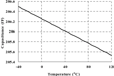
MOM capacitors are the two mostly used capacitors in RF systems, which have a temperature coefficient of 30-50 PPM/°C [15]. Figure 2 shows the simulated capacitance over a temperature range of -40~120 °C. As shown in Figure 2, one could argue that the temperature coefficient is about 30 PPM/°C. Thus, according to “𝑓 = 1
2𝜋√𝐿𝐶
⁄ ”, the frequency increases over
temperature range.
The other contributor in frequency drift is capacitor bank. The simple capacitor bank has been illustrated in Figure 3. This capacitor bank consists of transistor M1 and capacitor CA and CB. The ON/OFF states of the switch can affect frequency drift. When the switch is ON, the MOS transistor acts as a resistor with low resistance.
Therefore, the capacitors are connected in series and their dependency on temperature changes oscillat ing frequency. During OFF state, the MOS transistor is modeled by a high impedance.
Figure 2. Simulated capacitance vs. temperature range
Figure 3. Parasitic diode capacitors of transistor
Thus, the total capacitance is formed by the series combination of CA and parasitic diode capacitor Cdb (or CB and parasitic diode capacitor Csb). In this case, the total capacitance is determined by the parasitic diode capacitors. The parasitic diode capacitance is defined as [15]:
C jo Cdb Csb
n VR
1 ψ
o
(2)
where, Cj0, VR, and are PN junction capacitance, reverse bias voltage of PN junction and built-in potential, respectively. Since varies with temperature by -0.2 V/°C, the parasitic capacitance changes over temperature. Thus, according to “𝑓 = 1
2𝜋√𝐿𝐶
⁄ ”, the
VCO does not oscillate at the desired frequency range due to variation of capacitance.
2. 2. 2. Transistors Transistor has the most effect
on frequency drift due to the variation of its transconductance gain (gm), threshold voltage (Vth), mobility of electrons and holes (n and p) and parasitic capacitors. gm, Vth, andare obtained as follows [15]:
GS
m
ω
= μ Cn o V -V
g x th
L (3)
o
-V =-Vth th T-27 (4)
205.4 205.6 205.8 206 206.2 206.4 206.6
-40 0 40 80 120
C
a
pa
ci
ta
nce
(f
F
)
3
-T 2
° μ(T)= μ(T=27 )
° 27
(5)
where, µn, Cox, 𝜔
𝐿, VGS, Vtho, α, and T are mobility of electrons, silicon dioxide capacitor, size of transistor, Gate-Source voltage, threshold voltage, temperature coefficient of threshold voltage, and ambient temperature, respectively.
According to (3)-(5), by increasing temperature, the threshold voltage and mobility are reduced and subsequently gm decreases. The reduction in gm changes the level of harmonic distortion and oscillation frequency [7]. The simulated gm of NMOS transistor is demonstrated in Figure 4. As can be seen, the gm decrement is very significant. The parameter gm has a temperature coefficient of 1250 PPM/°C over a temperature range of -40~120 °C.
3. PROPOSED TEMPERATURE COMPENSATED CIRCUIT
Equations (2)-(5) show that the frequency increases by enhancing the temperature. Figure 5 shows the simulated frequency of the VCO without temperature
Figure 4. Simulated transconductance vs. temperature range
Figure 5. The simulated frequency vs. temperature range
compensation. As shown in Figure 5, the temperature drift is about 130 MHz. Also, the temperature coefficient of frequency is about 33.45 PPM/°C.
According to “𝑓 = 1 2𝜋√𝐿𝐶
⁄ ”, the oscillation
frequency, which is a drift from the desired frequency, can be compensated by changing the total inductance or capacitance seen from the output node. Changing the inductance is very difficult in integrated circuits. Also, inductor occupies a very large area in an IC. Thus, the best choice is changing the capacitance. Figure 6 describes the effect of temperature on frequency and its compensation. If the temperature rises and consequently it causes drop in the center frequency; it needs to decrease Ctotal for comensation. Also, if the temperature rises and consequently it causes rise in the center frequency; it needs to increase Ctotal for comensation. According to Figure 5 and 6, to compensate drift frequency, a temperature dependent voltage reference is needed to bias the varactors and change t heir capacitance and subsequently fix the oscillation frequency.
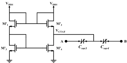
The proposed temperature compensation circuit has been depicted in Figure 7.
The voltage differences of the diode connections (transistor M′1-2) which are located at the top of the circuit produce a PTAT voltage. This PTAT voltage is applied to another diode connection (M′3) and this transistor is biased. The drain voltage of transistor M′3 becomes CTAT voltage. In addition, by mirroring the current of M′3, the drain voltage of the transistor M4 becomes CTAT. This voltage is applied to varactors and the values of varactors is enhanced. As mentioned, the frequency grew when the temperature was increased.
Figure 6. the effect of temperature on frequency and its compensation
Figure 7. Temperature compensation circuit.
135 140 145 150 155 160 165 170
-40 0 40 80 120
g
m
(m
S)
Temperature (°C)
24.2 24.24 24.28 24.32 24.36 24.4
-40 0 40 80 120
F
requency
(G
Hz
)
By employing a CTAT voltage circuit and biasing varactors with this CTAT voltage, the value of varactors augments and frequency increases. Therefore, the frequency drift over temperature is compensated.
4. DESIGN CONSIDRATIONS
4. 1. Sizes of Transistors The first important step
in designing an oscillator is to obtain the sizes of the transistors. In VCO design, to determine the sizes of transistors, it is necessary to consider the currents of the transistors. Since the transistors are in the saturation region, the sizes of NMOS transistors is defined as (7) [13].
W 2ID
=
2 L n μ C V -Vn ox GS thn
(7)
where, (W
L)nis sizes of NMOS transistors, ID is the drain
current, µn, is the electrons mubility, Vthn is threshold
voltages of NMOS, Cox and VGS are silicon dioxide
capacitor and gate-source voltage.
4. 2. Inductors To calculate the main frequency, it
is necessary to compute the inductance from the following equation [13]:
1
2 o
R f
L P
Q
(8)
where, Q is the quality factor of the inductor, Rp is the
equivalent parallel resistor of the inductor, and fo is the center frequency
.
The quality factor and Rp depend on the technology that is used and the inductance can be calculated by considering their values.4. 3. Oscilation Frequency and Start-Up Condition
After calculating the size of transistors from (7), the produced parasitic capacitors of transistors should be considered, since these capacitors affect oscillating frequency and the start-up condition. Furthermore, the inductor parasitic capacitors should also be considered. Thus, it is necessary to estimate all parasitic capacitances.
4. 3. 1. Inductor Capacitors The inductors that are
used in integrated circuits often have spiral form as shown in Figure 8 [14]. The equivalent circuit of these inductors is demonstrated in Figure 9 [15].
According to Figure 9, the values of capacitors, inductors, and resistors of this equivalent circuit are determined as follows. The values of inductors can be calculated as (9) [15].
(9) 2 2
37.5μ N a0 L=
11D-14a
Figure 8. Spiral inductor [13]
Figure 9. Equivalent circuit of the spiral inductor [13]
where, µ0 is the vacuum permeability, N is the number of inductor turns, a is the distance from the center of the inductor to the middle of the windings and D is the diameter of windings. The values of capacitors can be obtained from (10), (11) and (12) [15].
(10) εox
Cox= WL tox
(11) ε
2 ox C = NW Lp
tox
(12) 2
C =1 WLCsub
where, W, L, N, Csub, εox, and tox are metal width, total
length of the spiral, number of turns, body capacitance, silicon di oxide electrical permittivity and thickness of the oxide, respectively.
The values of resistors can be calculated using (13) and (14) [15].
(13)
LR =s
-t/δ Wσδ 1-e
(14) WLCsub
R =1 2
where, W, L,σ,Csub, t
,
andδ are metal width, total length of the spiral, conductivity of the metal, body capacitance, thickness of the metal and skin depth, respectively.is necessary to consider these capacitors. In application, gate-source capacitor and gate-drain capacitor are often considered, and other capacitors are neglected [15].
Since the transistors are in the saturation region, the values of these capacitors can be obtained as follows [15]:
(15)
2 CGS = CGSO+ CoxL W
3
(16) CGD = CGDO.W
where, CGD, CGS, CGSO, CGDO, and Cox are gate-drain, gate-source, gate-source overlap, gate-drain overlap and oxide capacitances, respectively.
4. 3. 3. Oscillation Frequency Analysis The
simplified equivalent half- circuit of the proposed VCO is illustrated in Figure 11. CL1, Cgd1, and Cgd3 are the parasitic capacitor of the inductor, gate-drain capacitors of NMOS and PMOS transistor, respectively. To derive the operation frequency, the transfer function between Vo and Vi is defined as (17).
(17) 3
3 2
gm L C C ω1 i o (C +C ) ωi o
L C C ω1 i o (C +C ) ωi o
[
]
[
]
Vo j
V i
where, Ci and Co are calculated as (18) and (19).
CiCL1+C +C1 gd1 (18)
CoCL1+CT1+Cgd3+CT2 (19)
Oscillation frequency will occur if loop gain of the circuit is unity, with a proper investigation, the oscillation frequency can be approximated as:
o
1 f
C Ci o 2π
C +Ci o
L
(20)
Figure 10. Capacitors of M OS transistor
Figure 11. Half equivalent circuit of the proposed VCO
From (18), (19) and (20) the oscillation frequency is adjusted by the voltage control, Vtune.
The start-up condition can be obtained from the following equation:
1
m P
g R (21)
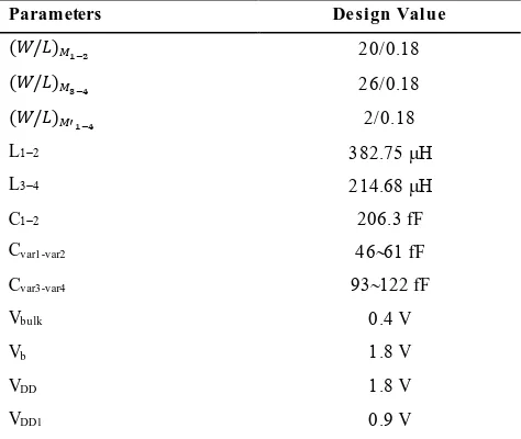
where, gm is transconductance of transistors and RP is the parallel resistor of the inductor. It is critical to consider this equation for maintaining oscillation. The circuit parameters of the proposed VCO are listed in Table 1.
5. SIMULATION RESULTS
In this paper, a temperature compensation VCO is introduced at 24.3 GHz and is designed and simulated (pre-layout) in Hspice software in 0.18 µm CMOS process technology. The Results show that power consumption of the VCO is 10.4 mW at the center frequency.
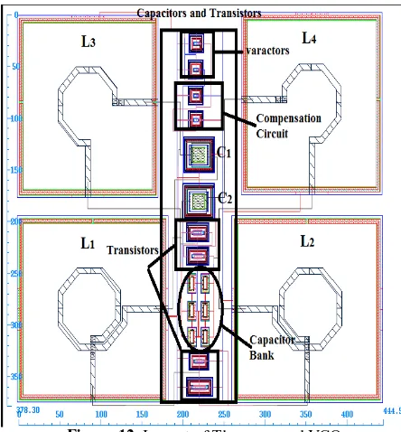
Figure 12 illustrates the layout of the circuit. As shown in Figure 12, the occupied area is 378 µm × 440 µm. This Figure illustrates that most of the IC space is occupied by inductors.
By employing temperature compensation circuit, the frequency drift becomes less. To prove this claim, the simulated center frequency over a temperature range of -40~120 °C, before and after temperature compensation have been shown in Figure 13. As demonstrated in Figure 13, before and after temperature compensation, the frequency drifts are 33.45 PPM/°C and 11.5 PPM/°C respectively. The proposed VCO has improved in terms of frequency drift about 65.6% (The frequency drifts before and after compensation are about 130 MHz and 45 MHz respectively).
TABLE 1. Circuit parameters of the proposed VCO
De sign Value Parameters
(𝑊/𝐿)𝑀1−2
(𝑊/𝐿)𝑀3−4
(𝑊/𝐿)𝑀′1−4
L
L
fF C
fF Cvar1-var2
fF Cvar3-var4
V Vbulk
V Vb
V VDD
Figure 12. Layout of The proposed VCO
Figure 13. Simulation of output frequency vs. temperature
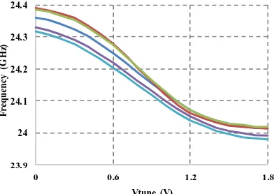
As demonstrated in Figure 14, the output frequency of the designed VCO can be tuned from 23.75 GHz to 24.8 GHz. Thus, the tuning range of the proposed VCO is 4.12%. This figure shows that the VCO covers a wide frequncy range by applying 2 varactors and a simple capacitor bank.
Based on simulation and Figure 15, the phase noise is -118.3 dBc/Hz and -102.6 dBc/Hz at 1 MHz frequency offsets before and after temperature compensation. By adding the temperature compensation circuit, the noise of this circuit affects output of the VCO and the phase noise performance deteriorates. This problem happens because of the transistors which are used at the temperature circuit have noise parameters. Even by considering this problem, the phase noise still acceptable at this frequency.
Figure 16 and Figure 17 illustrate the center oscillation frequency and phase noise by applying Monte Carlo analysis, which includes 50 samples at frequency of 24.35 GHz.
Figure 14. Frequency range of the proposed VCO in different states of switches
Figure15.The phase noise of the proposed VCO
Figure16. The simulated output frequency by M onte Carlo analysis
24.32 24.34 24.36 24.38 24.4 24.42 24.44 24.46 24.48
-40 0 40 80 120
F
re
que
nc
y
(G
Hz
)
Temperature(°C )
Without Temperature Compensation
With Temperature Compensation
23.7 23.9 24.1 24.3 24.5 24.7 24.9
0 0.6 1.2 1.8
F
req
ue
nc
y
(G
H
z)
Vtune (V)
-140 -130 -120 -110 -100 -90 -80 -70
0.1 1 10
P
ha
seN
o
is
e
(d
B
c/
H
z)
Frequency (MHz)
24.3 24.32 24.34 24.36 24.38 24.4 24.42 24.44
0 10 20 30 40 50
F
req
ue
nc
y
(G
H
z)
Figure 17. The simulated phase noise by M onte Carlo analysis
According to the results, the maximum likelihood of occurring oscillation frequency and phase noise are around 24.36 GHz and -101.4 dBc/Hz. Furthermore, Figures 18 and 19 demonstrate the frequency range and phase noise of the VCO in different modes of the corners. In normal mode, the frequency range is 24.05~24.35 GHz and center frequency has a phase noise of -101 dBc/Hz at 1 MHz offset frequency. In SS and FF corners, The frequency range of 24.05~24.35 GHz with -100.4 dBc /Hz phase noise and the frequency range of 23.98~24.32 GHz with a phase noise of 101.9 dBc / Hz at 1MHz offset frequency have been obtained, respectively. As shown in these figures, in addition to temperature, the proposed VCO has a good stability against process variation.
To compare the performance of the designed VCO with other works, a figure of merit (FOM) has been used. The FOM is defined as follows [12]:
(22)
0 DCoffset
offset
f P
FOM=L f -20log +10log
f 1mw
where, L{foffset} is the VCO phase noise, PDC is the dc power consumption and fo is the carrier frequency. The FOM of the VCO is -179.8 dBc/Hz.
Figure 18. The corners simulation of output frquency range
Figure 19. The corners simulation of phase noise
TABLE 2. Comparision with published work
[5] [6] [7] [8] This Work
Proce ss
0.18 µm SiGe BiCMOS
0.13 µm CMOS
0.18 µm CMOS
0.18 µm CMOS
0.18 µm C MO S
Fre quency
(GHz ) 3.65 2 2.4 19 24.35
Tuning
Range (%) 31 25 N/A 4.49 4.12
Phase Noise @ 1-MHz offset (dBc/Hz)
-116 -90.4 -115 -110 -102.6
DC Power
(mW ) 11.2 11.7 11.25 54 10.4
Te mperature
Range (°C) -30~90 -40~120 -40~100 N/A -40~120
Fre quency Inaccuracy (PPM/°C )
17.4 34 74 N/A 11.5
FO M
(dBc/Hz) -176.75 -145.73 -172.08 -178.3 -179.8
In the circuit analysis, all simulations related to the manufacturing process have been performed. So it is fair to compare them with measurement results.
Table 2 summarized some of the published works in the field of temperature compensation VCO design. It is observed that by using the compensation circuite and biasing it to varactors, this VCO can achieve minimized drift frequency while operates at the highest frequency. The temperature coefficient of the proposed VCO is better than other works, however the frequency of this VCO is higher than published works. Moreover, by employing Colpitts and Cross -Coupled pair structures, the power consumption of the proposed VCO is lower than other works. In addition, the proposed VCO has good phase noise performance at higher frequencies. -102
-101.8 -101.6 -101.4 -101.2 -101 -100.8 -100.6 -100.4
0 10 20 30 40 50
P
ha
seN
o
is
e
(dB
c/
Hz
)
Iteration
23.9 24 24.1 24.2 24.3 24.4
0 0.6 1.2 1.8
F
req
ue
nc
y
(G
H
z)
Vtune (V)
-140 -130 -120 -110 -100 -90 -80 -70
0.1 1 10
P
ha
seN
o
is
e
(d
B
c/
H
z)
Also, Table 2 shows that the proposed VCO outperforms other works in terms of FOM.
6. CONCLUSION
In this paper, a temperature compensation VCO based on Cross-Coupled pair and Colpitts structures has been designed and simulated in TSMC 0.18µm CMOS process. By employing this method, the phase noise and other performances are improved. To compensate the frequency drift over a temperature range, MOS varactors are used and biased with a CTAT voltage reference. The CTAT voltage reference and biasing it to varactors helps to have more stable frequency and phase noise versus temperature. By using this technique, the achieved temperature coefficient of the proposed VCO is 11.5 PPM/°C for temperature range of -40~120. In addition, based on simulation results, the phase noise of the proposed VCO is about -102.6 dBc/Hz at 1MHz offset frequency. Moreover, the VCO has 10.4 mW DC power consumption at 24.35 GHz frequency. The VCO covers frequencies of 23.75~24.8 GHz and the tuning range is 4.12%. Furthermore, the proposed VCO has FOM of -179.8 dBc/Hz.
7. REFERENCES
1. Loke, A. L. S., et. Al. “A Versatile 90 nm CMOS Charge Pump PLL for SerDes T ransmitter Clocking,” IEEE Journal of Solid-State Circuits, Vol. 41, No. 8, (2006), 1894-1907.
2. Seifi, S. et. Al. “ Analysis of Oscillation Amplitude and Phase Error in Multiphase LC Oscillators,” International Journal of Engineering, Transactions C: Aspects Vol. 26, No. 6 ,(2013) 587-596.
3. Nematzadeh, K. et. Al. “ A New Method of CMOS Ring Oscillator Analysis,” International Journal of Engineering, Transactions A: Basics Vol. 28, No. 1 (January 2015) 60-65. 4. M. Katebi, et. Al. “A Wide Tuning Range and Low Phase Noise VCO using New Capacitor Bank Structure”, Majlesi Journal of Electrical Engineering, Vol. 12, No. 4 (February 2018) 95-103.
5. M. Katebi, et. Al. "Low-power VCO for K-band Applications," Electrical Engineering (ICEE), Iranian Conference on, Mashhad, 2018, 144-149, (2018).
6. Akima, H., et. Al. “ A 10 GHz Frequency Drift T emperature Compensation LC VCO with Fast -Settling Low-Noise Voltage Regulator in 0.13 µm CMOS,” in 23th IEEE Custom Integrated Circuits Conference 2010, USA, 1-4, (2010).
7. Karri, S. R., et. Al. “ T emperature Compensated VCO design for Multi-band WCDMA T ransceiver Application,” in 3rd IEEE International Symposium on Radio-Frequency Integration T echnology2009, Singapore, (2009) 191-194.
8. Wu, G., et. Al. “ A Low-Voltage And T emperature Compensated Ring VCO Design,” in 10th Circuits and Systems Conference, (2014).
9. Wang, Y., et. Al. “A Temperature-Compensated LC Oscillator Using Constant -Biased Varactors,” IEEE Microwave and Wireless Components Letters, (2015) 130-132.
10. T ing, Y., Ming, Z. Y., Liang, L. H., Men, Z. Y. and Yue, W., “A K-Band Low Phase Noise and Wide Tunig Range LC VCO,” IEEE 12th International Conference on Solid-State and Integrated Circuit T echnology, Guilin, (2014).
11. Ravinuthula, V. and Finocchiaro, S., “ A Low Power High Performance PLL with T emperature Compensated VCO in 65nm CMOS,” in 20th Radio Frequency Integrated Circuits Symposium., USA , (2016).
12. Real, J. J. and Abidi, A. A., “ Physical processes of phase noise in differential LC Oscillator,” IEEE Custom Integrated Circuits Conference, Orlando, FL, (2000).
13. Razavi, B., "RF microelectronics, USA, Prentice Hall, (2011).. 14. Wang, T . P., “ A CMOS Colpitts VCO Using
Negative-Conductance Boosted T echnology,” IEEE Transaction on Circuits and System I, Vol. 58, No. 11, (2011), 2623-2635. 15. Allen, P. E. and Holberg, D. T., "CMOS Analog Circuit Design,
A Temperature Compensation Voltage Controlled Oscillator Using a Complementary
to Absolute Temperature Voltage Reference
M. Katebi, A. Nasri, S. Toofan, H. Zolfkhani
Integrated Circuits Laboratory, Electrical Engineering department, University of Zanjan, Zanjan, Iran
P A P E R I N F O
Paper history:
Received 12 September 2018
Received in revised form 05 March 2019 Accepted 03 May 2019
Keywords:
Colpitts
Complementary to Absolute Temperature Cross-coupled Pair
Temperature Compensation Voltage Controlled Oscillator
هدیکچ
نیا رد ناسون کی هلاقم اس
اب هارمه ژاتلو اب هدنوش لرتنک ز ناسون هیاپ رب یترارح یزاسناربج
جوز و ستیپلوک یاهزاس
یم هئارا یردبرض یم ،اهراتخاس نیا زا هدافتسا اب .دوش
رادم نیا .درک ادیپ تسد رتمک یفرصم ناوت و رتهب زاف زیون هب ناوت
رد یروانف 18 / 0 یس هیبش و یحارط سام تم نزاخ تفج کی زا یترارح یزاسناربج یارب .تسا هدش یزاس
هب هک ،ریغ
ژاتلو عبنم کی هلیسو CTAT
یم هیذغت یم لامعا روتکرو نزاخ ود هب عبنم نیا .تسا هدش هدافتسا ،دنوش ثعاب و دوش
رد سناکرف ندش رادیاپ هرتسگ
یم ییلااب ییامد هیبش .دوش
یم ناشن یزاس رد شور نیا زا هدافتسا اب هک دهد
هرتسگ ییامد
40 یلا 120 هجرد سویسلس بیرض ، تارییغت 5 / 11 هجرد رب نویلیم رد تمسق سویسلس
( PPM/C سناکرف رد )
یزکرم 35 / 24 یم تسد هب زترهاگیگ جیاتن هب هجوت اب .دیآ
هرتسگ ناسون نیا طسوت هدش هداد ششوپ یسناکرف لرتنک زاس
زا ژاتلو اب هدنوش 75
/ 23 یلا زترهاگیگ 8
/ 24 یم زترهاگیگ زاف زیون و یفرصم ناوت نینچمه .دشاب
رد و یزکرم سناکرف رد
تسفآ 1 ،زترهاگم 4 / 10 یلیم و تاو dBc/Hz 6 / 102 -یم یگتسیاش بیرض یراد هدش یحارط رادم .دنشاب dBc/Hz