Efficient Implementation of Low Power
CMOS Voltage Controlled Oscillator in PLL
T. Yugendra Chary 1, Ch. Satyanarayana 2
PG Research Scholar, Dept. of ECE, Sreenidhi Institute of Science and Technology, Hyderabad, TS, India1.
Assistant Professor, Dept. of ECE, Sreenidhi Institute of Science and Technology, Hyderabad, TS, India2.
ABSTRACT:PLL (Phased Locked Loop) is one of the important circuits in electronic communication and processing systems. Present days there is a huge demand for low power circuits.PLL consists of various blocks. One of the major blocks of PLL is VCO (Voltage controlled oscillator) and most of the PLL power is dissipated at VCO. This paper presents the design and implementation of low power CMOS VCO circuitry with the frequency range from 3GHz - 6GHz and reducing the power dissipation up to 20-25% by applying some low power techniques like Power Gating, Channel Tapering and Body Biasing.VCO is used for computer clock synchronization, demodulation and frequency synthesis. This project is designed using cadence software tool package (Virtuoso, ADE etc..) in 180nm technology.
KEYWORDS: PLL, VCO, Power Gating, Body Biasing and Channel tapering.
I. INTRODUCTION
Reducing power consumption and enhancing energy efficiency are the key issues in IC design. Lowering the supply voltage is the most effective way to achieve these goal and digital ICs operating at ultra- low voltages near threshold have been reported. In addition, optimal design of ,mixed signal circuits such as Phased Locked Loops(PLL) or Clock and Data Recovery (CDR) circuits operating at low supply voltages are attracting a significant amount of research interests.
PLL design for low-voltage application has many challenges and achieving supply-Noise immunity is very important [2]. Since supply voltage fluctuations can more seriously degrade the PLL performance at lower supply voltages. In particular, the Voltage controlled oscillator (VCO) is the most sensitive block to supply noise and can be the performance limiting factor for low voltage PLL [3]. Many circuit techniques that can reduce supply noise have been reported. However, these are not suitable for low voltage applications as they need additional transistors causing the voltage or require current mode logic (CML) which is not applicable in low voltage applications [17].
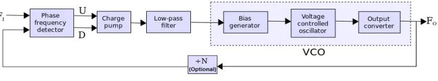
The block diagram of PLL is shown below.
Fig 1: PLL block diagram
VCO is considered as heart of the PLL, which plays a major role in it. The VCO block itself contain sub- blocks like Bias generator, VCO and output buffers.
the low power circuit designs saved a small amount of power up to a level of 10 to 15% by using various low power methods.
The main focus of this paper is on, to reduce the power dissipation of VCO by 20 to 25%, thereby designing a low power CMOS-VCO circuitry. This circuit is designed using 180nm technology. This circuit can produce the frequency range from 3GHz to 6GHz.
II. DESIGN & IMPLEMENTATION
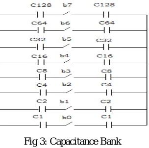
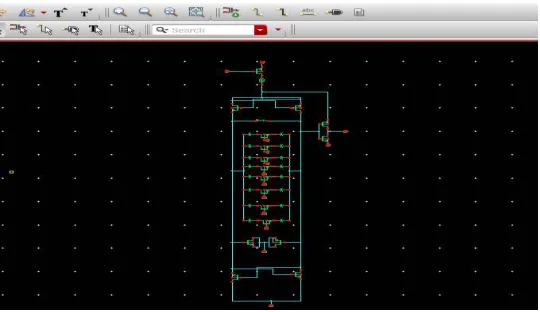
The schematic circuit of VCO is shown below. The major sections of VCO circuitry are Varactor diode, capacitance bank, cross-coupled PMOS and NMOS transistors and inverting buffers.
Fig 2: VCO schematic circuit. A. CAP BANK
In this VCO circuitry, 8-stage capacitance bank is used. With this, we can generate a wide range of frequencies. The selection of capacitance is done by enabling the switches. Here NMOS transistor is used as a switch. Here 8 switches are, based on the required capacitance applying a suitable pattern to the cap bank switches b0 to b7.
Ex: 00000000 to 11111111 to bob1b2b3b4b5b6b7
Fig 3: Capacitance Bank
B. VARACTOR DIODE
It is also called as Varicap. It’s a two terminal semiconductor PN junction diode which works under reverse bias where its junction capacitance is varied according to applied voltage. In this Varactor diode is implemented using transistor model.
Fig 4: Varactor diode
In this transistor model both the source and drain terminal are shorted and applied some required voltage based on the requirement of capacitance.
C. CROSS COUPLED CMOS TRANSISTORS
These are the both PMOS pair and NMOS transistor pairs are connected in a cross-coupled manner. Due to the presence of both PMOS and NMOS Transistors in VCO, hence this circuit is called as CMOS VCO. The cross-coupled transistors M1, M2, M3 and M4 are shown in Fig 2.
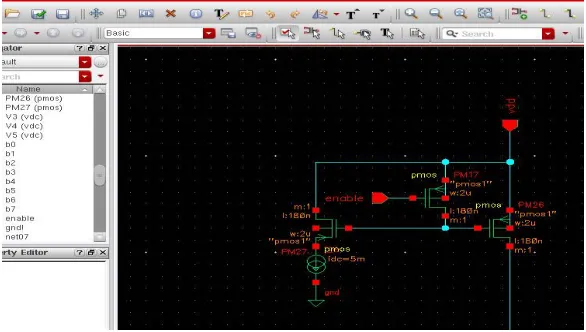
D. CURRENT BIASING CIRCUITRY
The current biasing and power enabling circuit is shown below. In this PMOS current mirror is used as a current biasing circuit. The biasing current is equal to 5mA.
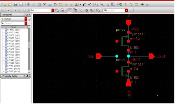
E. INVERTING BUFFERS
This is designed by using both PMOS and NMOS transistors. These inverted buffers are used to produce the Square wave while applying a sinusoidal wave nodes P and N. These nodes are having 1800 out of phase with the same magnitude. These also used for reproduction of proper voltage swings levels. The schematic of Inverted buffer is shown below.
Fig 6: Inverted Buffer
III. OPERATION OF VCO CIRCUIT
Let the oscillating node P is high with respect to node N, then it leads transistor M2 and M3 into the cut-off region and M1 will be turned ON and M4 also turned ON and they act like a short circuit and it draws maximum current from VDD. Then the cap bank and Inductor will gradual charging. Whenever their charges up to VDD, then M1 and M3 will be turned ON and make M2 and M3 turned OFF. Due to this gradual continuous charging and discharging they will start oscillating and producing a Sinusoidal waveform with certain frequency based on the values of Capacitance and Inductance. The sinusoidal waveform at node P and N are given to inverted buffers. They will convert the sinusoidal waveform into the square waveform. The outputs of both the inverters are 1800 out of phase and have the same magnitude.
IV. LOW POWER TECHNIQUES
A. POWER GATING
Power gating is a popular technique used in many synchronous circuits for reducing static power dissipation. By applying proper control signals to transistor gate terminal and we can enable or disable the VCO circuitry during the Active and idle modes.
Power gating technique is must require for this circuit because due to the positive feedback through cross-coupled CMOS transistor, there are a continuous charging and discharging of LC tank circuit. So it causes more power dissipation even in idle mode.
Hence this technique is applied to isolate VCO Core from the power supply and output nodes. The power gating is as shown in fig 7.
B. BODY BIASING
Body biasing is a technique where the substrate/wells on the die are biased to some voltage rather than GND (in case of NMOS) or VDD (in the case of PMOS). This technique works well to reduce channel sub-threshold leakage, does not do much for gate leakage and actually exacerbates junction leakage. It has little effect on dynamic power (the body biasing changes the source and drain junction capacitances to lower values).
This body biasing can be implemented by using two methods. They are 1. Fixed Biasing
2. Time-dependent biasing
If there is no proper Body biasing it affects the threshold voltage. This may affect the overall circuit performance.
Fig 7: Body Biasing to VCO core
In this Fixed biasing method is used. By using this technique, targeted to achieve power saving up to 10-15%. The amount of power saving by using this method is mentioned in power calculations and comparisons table.
C. CHANNEL TAPERING
Channel Tapering is the process of decreasing the size of each MOSFET transistor width along a serial chain such that the largest transistor is connected to the power supply and the smallest is connected to the output node.
In this work, it is demonstrated that in many cases tapering decreases delay and changes the shape of the output waveform such that the time during which a load inverter is conducting short circuit current is reduced. This decrease in short – circuit current also occurs in many cases where tapering does not offer a speed advantage. There is always a trade-off between these two. Hence in this tapering is done up to optimum level.
The main aim of this channel Tapering is to reduce the Propagation delay, power dissipation and physical area of VLSI circuits. By using this technique, targeted to achieve power saving up to 10-15%. The amount of power saving by using this method is mentioned in power calculations and comparisons table.
V. PARAMETER MEASUREMENTS RESULTS
A. FREQUENCY CALCULATIONS
Here the calculation of frequency is done at various values of Cap bank and inductor. The designed VCO is aimed to produce the frequency range from 3GHz to 6GHz. Here for the two instances frequency is calculated.
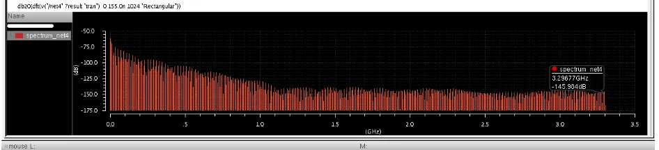
Fig. 9 VCO’s maximum signal frequency spectrums( fmax)
The obtained CMOS VCO’s maximum frequency spectrum is 5.807GHz at the values of inductance and capacitance are l= 10nH and c= 70 fF which is shown in fig 9.
fig: 10 VCO’s minimum signal frequency spectrum (fmin)
The obtained CMOS VCO’s minimum frequency spectrum is 3.29GHz at the values of inductance and capacitance are l= 10nH and c= 255fF. This is shown in above fig 10.
The achieved frequencies from the frequency spectrum are 3.29GHz and 5.807GHz at different values of cap bank. There is a slight variation in frequencies from the targeted one. This is mainly due to the presence of internal device junction capacitances and channel tapering but, these are negligible in terms of maximum usable frequency of any electronic device. The frequency spectrums of these frequencies are shown in fig 9, 10.
B. POWER CALCULATIONS
Fig11: Output Power Calculation window
In the above figure, the calculated power after applying body biasing and channel tapering, the total power dissipation is 322.6 uW which is shown in calculation window and the power dissipation after body biasing alone and with low power techniques are shown in stack sub- window as 366uW and 412uW respectively.
Power Comparisons
Here the power dissipation of CMOS-VCO circuitry at various level and after applying different low power techniques are expressed in a tabular manner and shown the comparisons with the percentage of power saving.
Table 1: Power comparisons
From the table, it is clear that the overall power dissipation of the low power CMOS VCO circuit is 412.4 uW, this can be further reduced by applying Body biasing (11.6% power saving ) along with channel tapering, the power consumption of the circuit is 322.6 uW.i.e., 21.84% of power is saved.
Parameter
Power consumption(uW)
% of power saving
Before applying
any technique 412.4 -
After applying body
biasing 366.4 11.16
After applying
VI. CONCLISION
The proposed Low power CMOS-VCO circuit is designed in 180nm Technology and generated the frequency range from 3GHz to 6 GHz with 8- stage Cap bank and using low power techniques like power gating, body biasing, and channel tapering and effectively reduced the power dissipation up to 21.84%.
REFERENCES
[1] Omar Abdelfattah, George Gal, Gordon W. Roberts, “A top - down Design Methodology Encompassing Components Variations Due To Wide-range Operation in Frequency Synthesizer PLLs,” Proc. IEEE Transaction on VLSI Systems, Volume: 24, Issue: 6, pages: 2050 - 2061, 2016. [2] Sung-Geun Kim, Jinsoo Rhim, Dae -Hyun Kwon; Min-Hyeong Kim; Woo Young Choi “A Low Voltage PLL With a Supply Noise
Compensated Feed forward Ring VCO,” IEEE Transactions on Circuits and Systems II, Volume: 63, Issue: 6 Pages: 548 - 552, 2016
[3] Amir Hossein Masnadi Shirazi; Amir Nikpaik; Reza Molavi; Sam Lightbody; Hormoz Djahanshahi;Mazhareddin Taghivand; Shahriar Mirabbasi; Sudip Shekhar “On the Design of mm-Wave Self-Mixing-VCO Architecture for High Tuning-Range and Low Phase Noise,” IEEE Journal of Solid-State Circuits, Volume: 51, Issue: 5, Pages: 1210 - 1222, 2016
[4] Sanjeev Jain; Sheng Lyang Jang; Nikolay T. Tchamov “Oscillation Mode Swapping Dual-Band VCO,” IEEE Microwave and Wireless Components, Volume: 26, Issue: 3, Pages: 210 - 212, 2016
[5] B.S.Cherkauer; EG.Friedman“Channel width tapering of serially connected MOSFET's with emphasis on power dissipation,” Volume: 2, Issue: 1, Pages: 100 - 114, 1994
[6] Sanjeev Jain; Sheng-Lyang Jang; Nikolay T. Tchamov “Tuned LC-Resonator Dual-Band VCO,” IEEE Microwave and Wireless Components,” Volume: 26, Issue: 3,Pages: 204 – 206, 2016
[7] To Po Wang “A K-Band Low-Power Colpitts VCO With Voltage-to-Current Positive - Feedback Network in 0.18 CMOS” IEEE Microwave and Wireless Components Volume:21, Issue: 4 Pages: 218 – 220, 2011
[8] Donguk Kim; Subin Choi; Jaehyouk Choi; Jae Joon Kim “A Reconfigurable Multiphase Ring Structure for Programmable Frequency Multiplication” IEEE Transactions on Circuits and Systems II, Volume: 62, Issue: 1,Pages: 51 - 55, 2015
[9] John A. McNeill; Rabeeh Majidi; Jianping Gong “Split ADCBackground Linearization of VCO-Based ADCs” IEEE Transactions on Circuits and Systems I Volume: 62, Issue: 1Pages: 49-58,2015
[10] TaehoSeong; Jae Joon Kim; Jaehyouk Choi “Analysis and Design of a Core-Size-Scalable Low Phase Noise VCO for Multi - Standard Cellular Transceivers” IEEE Transactions on Circuits and Systems I, Volume: 62, Issue: 3Pages: 781 - 790, 2015
[11] P. Vaananen; N. Mikkola; P. Helio “VCO Design With On-Chip Calibration System” IEEE Transactions on Circuits and Systems I, Volume:
53, Issue: 10Pages: 2157 - 2166, 2006
[12] Ho-Jun Chang; Changwoo Lim; Tae-Yeoul Yun “CMOS QVCO With Current-Reuse, Bottom-Series Coupling, and Forward Body Biasing Techniques” IEEE Microwave and Wireless Components Volume: 24, Issue: 9Pages: 608 – 610, 2014
[13] K. M. Mahfuzul Islam; Hidetoshi Onodera “On-chip monitoringand compensation scheme with fine-grain body biasing for robust and energy-efficient operations” 21st Asia and South Pacific Design Automation Conference (ASP-DAC),Pages: 403 - 409, 2016
[14] Taeho Seong; Jae Joon Kim; Jaehyouk Choi “Analysis and Design of a Core-Size Scalable Low Phase Noise VCO for Multi Standard Cellular Transceivers” IEEE Transactions on Circuits and Systems I, Volume: 62, Issue: 3, Pages: 781 – 790, 2015
[15] Taimur Rabuske; Jorge Fernandes “A 12-bit SAR ADC with background self-calibration based on a MOSCAP-DAC with dynamic body-biasing” IEEE International Symposium on Circuits and Systems (ISCAS), Pages: 1482 – 1485, 2016
[16] Sudhanshu Choudhary, Shafi Qureshi “Power aware channel width tapering of serially connected MOSFETs” International Conference on Microelectronics, Pages: 399-402, 2007