PHYS 331: Junior Physics Laboratory I
Notes on Digital Circuits
Digital circuits are collections of devices that perform logical operations on two logical states, represented by voltage levels. Standard operations such as AND, OR, INVERT, EQUIVALENT, etc. are performed by devices known as gates. Groups of compatible gates can be combined to make yes/no decisions based on the states of the inputs. For example, a simple warning light circuit might check several switch settings and produce a single yes/no output. More complicated circuits can be used to manipulate information in the form of decimal digits, alphanumeric characters, or groups of yes/no inputs. These notes are intended to familiarize you with the elementary principles of this field.
A. Analysis of asynchronous logic
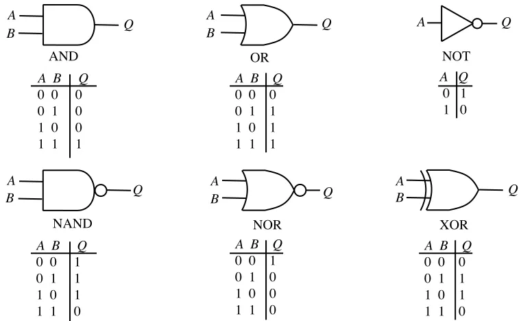
Suppose we have a statement which can be true or false, perhaps representing the presence or absence of a particle, a light signal on or off, a voltage present or absent, or any other binary possibility. For now we will ignore the physical meaning of the statement and ask how one would decide the logical truth or falsehood of combinations of such statements, a subject called combinatoric logic. If we denote the "truth value" of a statement A by 0 or 1, the standard combinations are shown in the form of "truth tables" in Fig. 1. These basic combinations, or
A B Q 0 0 0 0 1 0 1 0 0 1 1 1 AND A
B Q
A B Q 0 0 0 0 1 1 1 0 1 1 1 1 OR A
B Q A
A Q 0 1 1 0 NOT
A B Q 0 0 1 0 1 1 1 0 1 1 1 0 NAND A
B Q
A B Q 0 0 1 0 1 0 1 0 0 1 1 0 NOR A
B Q
A B Q 0 0 0 0 1 1 1 0 1 1 1 0 XOR A
B Q
similar ones, have been implemented in electronic circuitry, where truth values can be represented by different voltage levels. The standard circuit symbols are also shown in Fig. 1.
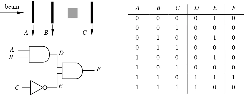
By combining the basic operations we can construct other logical functions. For example, suppose we wish to determine whether or not a particle has stopped in a target, using the configuration of counters shown in Fig. 2. A particle passing through a counter makes the corresponding output true, and we assume the particle has stopped in the target if A and B are both true, but C is false. Formally, we want to know when the compound statement A•B•C is true. An electronic implementation of the compound statement is also shown in Fig. 2, together with a truth table. Examination of the truth table shows that A•B•C is true in exactly one situation, which corresponds to the physically desired result.
Sometimes it is not obvious how to write down the required expression and implement it. You might discover an implementation using only standard operations by trial and error, but it is possible to be more systematic. For example, suppose we wish to make an exclusive-OR function using AND, OR and NOT gates. To do this we can try to combine some statements that are true for exactly one combination of A and B. Consider the following:
A•B is true only when A = 1 and B = 1
A•B is true only when A = 1 and B = 0 (1) A •Bis true only when A = 0 and B = 1
A •B is true only when A = 0 and B = 0
The middle two lines are the A,B values for which the X-OR is true, so if we combine them with an OR, we get the desired result,
A B C
beam
A B
C
D
E
F
A B C D E F
0 0 0 0 1 0
0 0 1 0 0 0
0 1 0 0 1 0
0 1 1 0 0 0
1 0 0 0 1 0
1 0 1 0 0 0
1 1 0 1 1 1
1 1 1 1 0 0
A!B=
(
A •B)
+(
A•B)
(2)This procedure, combining AND statements which are true for the desired true outputs, is actually quite general, although it may generate very cumbersome expressions.
It is sometimes desirable to transform a logical expression to some other form, perhaps to simplify implementation or to take advantage of the devices available in a particular logic family. Fortunately, the logical operators define an algebra, usually referred to as Boolean algebra. The familiar commutative, associative and distributive properties hold:
A+B=B+A A•B=B•A (3)
A•
(
B•C)
=(
A•B)
•C A+(
B+C)
=(
A+B)
+C (4)A•
(
B+C)
= A•B+A•C (5)so one can use the normal rules of algebraic manipulation on logical expressions. Two theorems, called DeMorgan's laws are particularly useful:
A+B=A •B A•B= A +B (6)
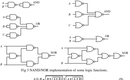
As an example, suppose we wish to implement the exclusive-or expression using NAND gates, which compute A•B. We first attack the A•B term by adding zero, using the distributive law and then applying DeMorgan's law:
A•B =A• B +A• A
=A•
(
A +B)
=A•
(
A•B)
(7)
Doing the same with A •B, we arrive at
A!B=
[
B•(
A•B)
]
+[
A•(
A•B)
]
(8)A!B=
[
B•(
A•B)
]
•[
A•(
A•B)
]
(9)which is the desired expression in terms of NAND functions. This circuit is shown in Fig. 3, along with several other examples.
Synthesis of desired logic functions can obviously become quite complex. Fortunately there are far more sophisticated techniques available. Some of these can be found in the book by Horowitz and Hill, and others in electrical engineering texts.
B. Time dependence
In certain systems timing may become critical. Gates require a finite amount of time to change their output in response to a change in the input signals (gate delay). In a complicated circuit it may happen that the inputs to a particular gate have been processed through different numbers of preceding stages, and may not arrive at the same time. This will cause the last gate to produce an electrically correct but logically wrong output, at least transiently. In situations where this causes problems it can be cured either by accurate matching of the signal delays, or by clocking.
The matching approach is used where the logic must handle events in "real time", as required in a particle-counting experiment. The method is to add delay as needed to insure that all possible signals require the same amount of time to propagate through each stage in the system. Timed logic circuits are sometimes called "combinational" or "asynchronous" logic,
A B
AND
OR
A
B
C
A
B
XOR
AND
OR
XOR
A
B A B A
B
C
since they produce an output as quickly as possible after a change in input. Such circuits are obviously very difficult to adjust if they are at all complex.
The alternative to asynchronous logic is "synchronous" or "clocked" logic. In this scheme an additional input, the clock, is provided at each logical stage. The circuits are designed to accept input on, say, a low to high transition of the clock signal and to change output state on the following high to low transition. This scheme always leads to valid inputs at each successive stage as long as the clock period is longer than the longest propagation delay in the system. The timing problem is then reduced to distributing the clock signal synchronously to all stages, at the cost of a slower response to the inputs.
C. Flip-flops and counters
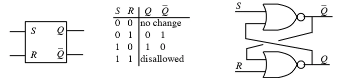
Flip-flops are circuits that can be put into one of two stable states with a pulse applied to a specified input. The circuit then remains in that state until another pulse is received. This constitutes a form of memory, in that the circuit "remembers" that a pulse was applied sometime in the past. An obvious application is in computer memory chips, where millions of flip-flops are put on a single integrated circuit.
The truth table for a simple example, called a set-reset (SR) flip-flop is shown in Fig. 4, together with a realization using NOR gates. The operation of the SR can be understood by reading through the truth table. If both S and R inputs are zero, the Q and Q outputs retain whatever state they are in. If either S or R goes to 1, Q and Q change to the values indicated and remain in that state when S or R returns to zero. If both S and R go to 1 the output is indeterminate, so that combination of inputs is not allowed.
The limitations of the SR flip-flop led to the development of several other types, of which only the JK shown in Fig. 5 will be examined here. As indicated by the truth table, the J and K inputs function like the S and R inputs to force a particular state of the flip-flop. A crucial difference is that Q changes only after a pulse at the CLOCK input, and that the state is retained until another pulse arrives, regardless of the J or K values. Holding both J and K in the true state allows the flip-flop to be toggled between its two states by applying pulses to the single clock input.
S
R Q
Q_
S R Q Q
0 0 no change 0 1 0 1 1 0 1 0 1 1 disallowed
Q
Q
_
S
R
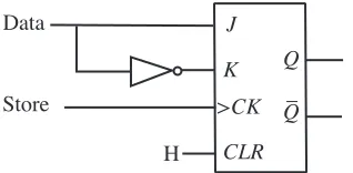
Since a JK flip-flop can hold a state, it is the basis of a one-bit memory, as illustrated in Fig. 6. A pulse applied to Store causes Q to switch to the value at the input data line Data, and hold the value until the next clock pulse. A group of flip-flops can be used to store several bits of data on command, and is called a data latch or memory register.
A binary counter can be made by connecting the output of one flip-flop to the clock input of another. If the flip-flops are all configured to toggle, a chain of n flip-flops will have 2n different output states. Each clock pulse arriving at the first flip-flop will either increment or decrement the output state by one unit, depending on the device used. A counter can be used to count the number of clock pulses arriving in a certain interval, to divide an input frequency by n, or to provide one output pulse for 2n input pulses. (These last two applications are why counters are sometimes referred to as dividers.) Standard ICs often provide additional inputs to set the counter to a specific state, such as all-zeros, or to control the direction of counting.
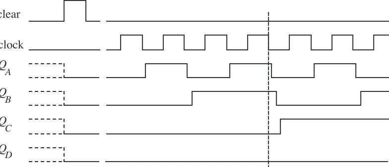
Since counters and flip-flops have inherent time dependence, truth tables do not provide sufficient information about when changes of logic state occur. They can be supplemented by a timing diagram, as given in Fig. 7 for a typical binary counter. Using the diagram, one can decipher how the outputs QA...QD respond to pulse inputs on the "clear" and "clock" lines. Note,
for example, that QA always changes state on the falling (1!0) edge of the clock pulse.
CLEAR CLOCK J K Q Q_ L X X X L H H
H H H
L L H L L H H H
Q Q H L L H TOGGLE
0 0 _ J
K Q
Q CLR >CK _
Fig. 5 Circuit symbol and truth table for a JK flip-flop. The X means "don't care", in that setting CLEAR low will force Q low regardless of other inputs.
J
K Q
Q CLR >CK _ Data
Store
H
A more subtle timing issue is that there is a delay (see Table I) between the edge of the clock pulse and the change in Q at each stage. These delays accumulate across stages, and may result in an output count which is wrong until the change propagates through the last stage. A delay of tens of nanoseconds to get the correct output would not affect human-read displays, but might cause trouble with further logic circuits. Some counter chips are therefore designed to be synchronous, using an internal signal to ensure that all outputs change to the final state together.
D. Logic families
There are a number of commonly-available electronic logic families, as summarized in Table I. (NIM logic is a special case included for completeness. It will be considered more fully in the section on particle counting.) As you can see, the types differ in their elementary function and in whether they respond to current or voltage signals. Fan-out refers to the ability of an output to drive more than one subsequent input, but this is not usually a problem. From a design perspective, the speed of operation is often a deciding factor, along with cost and the ability to construct very complex single-chip circuits (Very Large Scale Integration).
You should also be aware that there are many ready-made functions available in each of the commercial logic families. These typically include multi-input gates, flip-flops, adder circuits and even complete CPUs. There are also compatible interface circuits, such as display drivers, transmission line drivers, analog to digital converters and so on. For reasons of simplicity and reliability, you should make use of specialized units whenever possible.
It is highly unlikely that you will ever need to build a logic function out of discrete transistors, resistors etc., so for the present we will treat the circuits as black boxes. If you do a
clear
clock
Q Q
Q Q A
B
C
D
lot of digital design you should gain at least a rough idea of how the functions are carried out by the internal circuitry, since that will help you use the building blocks more effectively.
It is highly unlikely that you will ever need to build a logic function out of discrete transistors, resistors etc., so for the present we will treat the circuits as black boxes. If you do a lot of digital design you should gain at least a rough idea of how the functions are carried out by the internal circuitry, since that will help you use the building blocks more effectively.
E. Connecting gates
In real logic systems one wants to connect several gates together, so we need to examine what happens when we do this with the TTL circuits used in our lab exercises. When an output at logic high, +5V, is connected to the input of a similar gate a small current will flow due to the leakage currents of the input transistor in the driven gate. Since leakage currents are fairly small, a TTL gate can in fact drive several inputs into the "high" logic range. The situation is a little different for a low signal, since significant current must flow out of the driven input to hold it within the "low" range. The output stage of the driving gate does this by turning on its output transistor, thereby providing a relatively low-impedance path to ground. As a practical matter, though, the transistor in the driving gate can only pass so much current, and this limits the
Table I. Summary of Gate Characteristics Gate Type
Charac. TTL ECL CMOS NIM(neg) NIM(pos) Basic func. NAND OR,NOR NOR - -
Connection Current Voltage Voltage Current Voltage Logic 0 0.0 ! 0.8V -0.9V 0 ! 2V +1 ! -2mA 1.5 ! -2V 1 2.5 ! 5.0V -1.8V 7 ! 10V 4 ! 12mA 3 ! 12V Fan-out 10 25 10-20 1 1-2 Gate delay 15ns 3ns 70ns 10ns 500ns Advantages Standard Fast Low power Modules Modules
Cheap Very cheap Flexible Flexible Noise VLSI Z=50"
immunity
number of inputs that one circuit can drive to about 10. Similar considerations determine the number of inputs that each output can drive in the other logic families.
In general, the drive capability of a gate is called the "fanout". Within one logic family (TTL, ECL, CMOS, NIM ...) an output will always drive inputs up to the fanout, so electrical compatibility is assured simply by counting inputs. Connections can sometimes be made between families if the electrical characteristics are well understood, but it is usually necessary to use special devices to "translate" logic levels.
It is sometimes tempting to connect several outputs to one input in the hope of getting some sort of summing action, but this is unlikely to work. Consider the situation where two outputs are connected with one in a low state and the other high. The low output is trying to pull the connection low, but the high output and the input of the next gate will supply substantial current, perhaps exceeding the current sinking capability of the low output. Even if no damage occurs, the result is likely to be abnormal logic levels and unpredictable results.
F. Conversion circuits
For digital logic to be useful in many applications there must be a transformation to or from continuously-variable "analog" signals. This function is the province of digital to analog, D/A, or analog to digital, A/D, converters. The actual design of such circuits demands complex tradeoffs among cost, speed and a multiplicity of possible error sources. Here we will mention some of the basic principles so that you can rationally choose a commercial module when you need it.
The goal of a D/A is to convert a multi-bit binary number to a proportional voltage or current. General purpose schemes typically involve switching voltage or current sources on or off under digital control and adding the results. One example is shown in Fig. 8, in which a
-+
R
Vo
Vref R R R 2R
2R 2R 2R 2R
MSB LSB
cleverly-chosen resistor network provides a voltage proportional to the input number. A unity-gain amplifier buffers the resistor network from whatever load we wish to connect. The accuracy and speed of conversion will depend on resistor tolerances, the quality of the digitally-controlled switches, and the properties of the amplifier.
Analog to digital converters come in more varieties than D/As, but most designs depend on a comparator. The comparator circuit accepts a reference voltage and the unknown voltage, and produces a logical one output when the unknown exceeds the reference. The simplest A/D implementations provide a reference voltage corresponding to each digital output and use one comparator for each level. Logic circuitry determines the highest-level comparator that is at logic one and produces a corresponding binary code. These parallel or "flash" converters are fast, but become too cumbersome when high accuracy is needed. They do find use where speed is paramount, as in reading out tracking chambers in high energy physics experiments.
Successive-approximation converters use only one comparator in combination with a D/A converter. The D/A is given a digital code and the output is compared to the unknown voltage. The largest digital code that does not exceed the unknown is taken as the digital output value. The conversion obviously takes time, but by using a binary search sequence only n trials are needed for n-bit output, enabling a typical module to produce an eight to twelve bit conversion in a few microseconds.