BASIC NON
PIPELINED CPU
ARCHITECTURE
Central Processing Unit
◦Introduction
◦ 3 major parts of CPU :
◦1) Register Set
◦2) ALU
◦3) Control
3 types of CPU organizations
◦1) Single AC Org. : ADD X
◦2) General Register Org. : ADD R1, R2, R3
◦3) Stack Org. : PUSH X
] [X M AC
AC
3 2 1 R R
R
The importance of register
◦ Memory locations are needed for storing pointers, counters, return address,
temporary results, and partial products during multiplication
◦ Memory access is the most time-consuming operation in a computer
◦ More convenient and efficient way is to store intermediate values in processor registers
Bus organization for 7 CPU registers :
◦ 2 MUX : select one of 7 register or
external data input by SELA and SELB
◦ BUS A and BUS B : form the inputs to a common ALU
◦ ALU : OPR determine the arithmetic or logic micro operation .
The result of the micro operation is available for external data output and also goes into the inputs of all the
registers
◦ 3 X 8 Decoder : select the register (by
SELD) that receives the information from ALU
External Output External Input
General Register Organization
R 1 R 2 R 4 R 3 R 6 R 7 R 5
3 × 8 d e c o d e r
M U X M U X
A rith m e tic lo g ic u n it ( A L U )
C lo c k In p u t
L o a d ( 7 lin e s )
S E L A S E L B
A b u s B b u s
O P R
O u tp u t S E L D
( a ) B lo c k d ia g ra m
( b ) C o n tro l w o rd
S E L A S E L B S E L D O P R
Detailed data path of a typical
register based CPU
R 1 R 2 R 4 R 3 R 6 R 7 R 5
3 × 8 d e c o d e r
M U X M U X
A rith m e tic lo g ic u n it ( A L U )
C lo c k In p u t
L o a d ( 7 lin e s )
S E L A S E L B
A b u s B b u s
O P R
O u tp u t S E L D
( a ) B lo c k d ia g ra m
( b ) C o n tro l w o rd
S E L A S E L B S E L D O P R
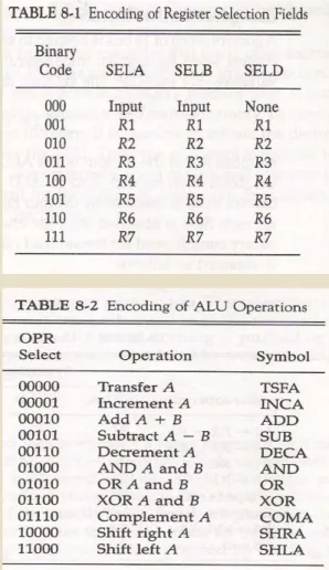
◦ Binary selector input :
◦ 1) MUX A selector (SELA) : to place the content of R2 into BUS A
◦ 2) MUX B selector (SELB) : to place the content of R3 into BUS B
◦ 3) ALU operation selector (OPR) : to provide the arithmetic addition R2 + R3
◦ 4) Decoder selector (SELD) : to transfer the content of the output bus into R1
◦ Control Word
◦ 14 bit control word (4 fields) :
◦ SELA (3 bits) : select a source register for the A input of the ALU
◦ SELB (3 bits) : select a source register for the B input of the ALU
◦ SELD (3 bits) : select a destination register using the 3 X 8 decoder
◦ OPR (5 bits) : select one of the operations in the ALU
◦ SELA or SELB = 000 (Input) : MUX selects the external input data
◦ SELD = 000 (None) : no destination register is selected but the contents of the output bus are available in the external output
◦ Encoding of ALU Operation (OPR) : Tab. 8-2
◦ Examples of Micro operations :
◦ TSFA (Transfer A) :
Tab. 8-1
Tab. 8-2
General Register Organization
3 2 1 R R R
Input External Output External R Output External R
◦ Stack Organization
◦ Stack or LIFO(Last-In, First-Out)
◦ A storage device that stores information
◦ The item stored last is the first item retrieved = a stack of tray
◦ Stack Pointer (SP)
◦ The register that holds the address for the stack
◦ SP always points at the top item in the stack
◦ Two Operations of a stack : Insertion and Deletion of Items
◦ PUSH : Push-Down = Insertion
◦ POP : Pop-Up = Deletion
◦ Stack
◦ 1) Register Stack Fig. 1
◦ a finite number of memory words or register(stand alone)
◦ 2) Memory Stack
◦ a portion of a large memory
Stack Organization
◦ Memory Stack : Fig. 2
◦ PUSH
◦ POP
◦ Stack Limits
◦ Check for stack overflow(full)/underflow(empty)
◦ Checked by using two register
◦ Upper Limit and Lower Limit Register
* Error Condition PUSH when FULL = 1 POP when EMTY = 1
Stack Organization
Accumulator architecture
Example code: a = b+c;
load b; add c;
store a;
Accumulator
ALU
Memory
registers
address
latch
Stack architecture
Example code: a = b+c;
push b; push c; add; pop a;
b
b
c
b+c
push b push c add pop a
stack:
ALU
Memory
stack
stack pt
latch
latch
Other architecture styles
Stack
Architecture
Accumulator
Architecture
Register-Memory
Memory-
Memory
Register
(load-store)
Push A Load A Load r1,A Add C,B,A Load r1,A
Push B Add B Add r1,B Load r2,B
Add Store C Store C,r1 Add r3,r1,r2
Pop C Store C,r3
Other architecture styles
◦
Accumulator architecture
◦ one operand (in register or memory), accumulator almost always implicitly used
◦
Stack
◦ zero operand: all operands implicit (on TOS)
◦
Register (load store)
◦ three operands, all in registers
◦ loads and stores are the only instructions accessing memory (i.e. with a memory (indirect) addressing mode
◦
Register-Memory
◦ two operands, one in memory
◦
Memory-Memory
The fetch-decode-execute cycle
Generic Steps:
1. FETCH: Fetch and Increment PC 2. DECODE: Decode and Read Registers 3. EXECUTE
4. MEMORY ACCESS
Control Unit Implementation
In this case, the control unit is a combinatorial
circuit; it gets a set of inputs (from IR, flags, clock, system bus) and transforms them into a set of
control signals.
• Hardwired control provides highest speed.
• RISCs are implemented with hardwired control. • If the instruction set becomes very complex
(CISCs) implementing hardwired control is very
Control Unit Implementation
Microprogrammed control - basic idea:
• All microroutines corresponding to the machine instructions are stored in the control store.
• The control unit generates the sequence of control
signals for a certain machine instruction by reading
from the control store the CWs of the microroutine
TERMINOLOGY
Microprogram
- Program stored in memory that generates all the control signals required to execute the instruction set correctly
- Consists of microinstructions
Microinstruction
- Contains a control word and a sequencing word
Control Word - All the control information required for one clock cycle
Sequencing Word - Information needed to decide
the next microinstruction address
- Vocabulary to write a microprogram
Sequencer (Microprogram Sequencer)
A Microprogram Control Unit that determines
Microprogram Sequencer
◦
The basic components of microprogrammed control unit
are the
control memory
circuits that select the next address.
◦
The task of Microinstruction sequencing is done by
Microprogram sequencer
.
◦
The address selection part is called as
microprogram
sequencer
.
The purpose of
microprogram sequencer
is to present an
MUX 1 SBR
Incrementer
CAR Input
Logic
MUX 2
Select
Control Memory
Microprogram sequencer for a control Mmemory
Microprogram Sequencer
Microprogram Sequencer
◦
The purpose of
microprogram sequencer
is to
present an address to the control memory so that a
microinstruction may be read and executed.
◦
The
next address logic
of the sequencer determines
the specific address source to be loaded into the
CAR.
◦
The choice of the address source is guided by the
next address information bits
that the sequencer
receives from the present microinstruction.
◦
There are two multiplexers in the circuit.
Microprogram Sequencer
◦
The second multiplexer tests the value of a
selected status bit and the result of the test is
applied to an input logic circuit.
◦
The output from CAR provides the address for the
control memory.
◦
The contents of CAR is incremented and applied to
one of the multiplexer inputs and to the SBR.
◦
The other three input come from the address field
of the present microinstruction, from the output of
SBR and from an external source that maps the
PIPELINING
R1 Ai, R2 Bi Load Ai and Bi
R3 R1 * R2, R4 Ci Multiply and load Ci R5 R3 + R4 Add
A technique of decomposing a sequential process
into suboperations, with each subprocess being
executed in a partial dedicated segment that
operates concurrently with all other segments.
Ai * Bi + Ci for i = 1, 2, 3, ... , 7
Ai
R1 R2
Multiplier
R3 R4
Adder
R5
Memory
Bi Ci Segment 1
Segment 2
OPERATIONS IN EACH PIPELINE
STAGE
Clock
Pulse Segment 1 Segment 2 Segment 3
Number R1 R2 R3 R4 R5 1 A1 B1
2 A2 B2 A1 * B1 C1
3 A3 B3 A2 * B2 C2 A1 * B1 + C1 4 A4 B4 A3 * B3 C3 A2 * B2 + C2 5 A5 B5 A4 * B4 C4 A3 * B3 + C3 6 A6 B6 A5 * B5 C5 A4 * B4 + C4 7 A7 B7 A6 * B6 C6 A5 * B5 + C5 8 A7 * B7 C7 A6 * B6 + C6
GENERAL PIPELINE
General Structure of a 3-Segment Pipeline
S1 R1 S2 R2 S3 R3 Input
Clock
Space-Time Diagram
1 2 3 4 5 6 7 8 9