An Introduction to Nanoscience
and Nanotechnology
An Introduction to Nanoscience
and Nanotechnology
Part of this book adapted from “Introduction aux nanosciences et aux nanotechnologies” published in France by Hermes Science/Lavoisier in 2006
First published in Great Britain and the United States in 2008 by ISTE Ltd and John Wiley & Sons, Inc. Apart from any fair dealing for the purposes of research or private study, or criticism or review, as permitted under the Copyright, Designs and Patents Act 1988, this publication may only be reproduced, stored or transmitted, in any form or by any means, with the prior permission in writing of the publishers, or in the case of reprographic reproduction in accordance with the terms and licenses issued by the CLA. Enquiries concerning reproduction outside these terms should be sent to the publishers at the undermentioned address:
ISTE Ltd John Wiley & Sons, Inc. 6 Fitzroy Square 111 River Street London W1T 5DX Hoboken, NJ 07030
UK USA
www.iste.co.uk www.wiley.com
© ISTE Ltd, 2008 © LAVOISIER, 2006
The rights of Alain Nouailhat to be identified as the author of this work have been asserted by him in accordance with the Copyright, Designs and Patents Act 1988.
Library of Congress Cataloging-in-Publication Data Nouailhat, Alain.
An introduction to nanoscience and nanotechnology / Alain Nouailhat. p. cm.
"Part of this book adapted from "Introduction aux nanosciences et aux nanotechnologies" published in France by Hermes Science/Lavoisier in 2006."
Includes bibliographical references. ISBN 978-1-84821-007-3
1. Nanoscience. 2. Nanotechnology. I. Title. QC176.8.N35N68 2007
620'.5--dc22
2007021734 British Library Cataloguing-in-Publication Data
A CIP record for this book is available from the British Library ISBN: 978-1-84821-007-3
The Physicists
“Leaning over the screens of powerful machines They watch the rise of a world previously unknown From within their instruments new phenomena appear.”
Table of Contents
Foreword. . . xiii
Acknowledgements . . . xv
Preface. . . xvii
Chapter 1. What are Nanos?. . . 1
1.1. What are we talking about?. . . 3
1.2. References. . . 7
1.2.1. Two basic facts . . . 7
1.2.2. Two approaches . . . 9
1.2.3. Two key points . . . 11
1.3. Some bonus material for economists. . . 13
Chapter 2. Some Science to Get You Started. . . 15
2.1. Quantum physics . . . 17
2.1.1. From the traditional world to the quantum world . . 17
2.1.2. Two fundamental concepts . . . 19
2.1.2.1. Wave-corpuscle duality . . . 19
2.2. The key players . . . 22
2.2.1. The electron . . . 22
2.2.1.1. The cornerstone of matter . . . 22
2.2.1.2. Electronic states . . . 23
2.2.1.3. The quantification of energy . . . 24
2.2.1.4. Bonds . . . 25
2.2.2. The photon . . . 27
2.2.2.1. The wave. . . 27
2.2.2.2. The energy grain . . . 30
2.3. Molecules . . . 34
2.3.1. From the smallest molecule to the largest and their spectacular properties . . . 34
2.3.2. Functionality . . . 35
2.4. Solid matter . . . 36
2.4.1. Insulators or conductors. . . 36
2.4.2. Semi-conductors . . . 37
2.4.2.1. Silicon crystal. . . 37
2.4.2.2 Electrons and holes. . . 40
2.4.2.3 Junctions . . . 40
2.4.3. Nanomaterials . . . 41
2.5. Quantum boxes: between the atom and the crystal. . . 41
2.6. Some bonus material for physicists. . . 42
2.6.1 Luminescence . . . 42
2.6.2. The laser device . . . 44
Chapter 3. The Revolution in Techniques Used in Observation and Imagery. . . 51
3.1. Observing with photons . . . 53
3.1.1. The optical microscope in visible light . . . 53
3.1.2. X-ray machines . . . 54
3.2. Observing with electrons . . . 55
3.2.1. The transmission electron microscope (TEM) . . . . 55
3.3. Touching the atoms . . . 58
3.4. Observing how our brain functions. . . 60
3.4.1. Nuclear magnetic resonance . . . 60
3.4.2. Functional magnetic resonance imaging . . . 61
3.5. Some bonus material for researchers. . . 62
Chapter 4. The Marriage of Software and Hardware. . . 69
4.1. Small is beautiful . . . 71
4.2. Miniaturization. . . 71
4.3. Integration. . . 72
4.3.1. The silicon planet . . . 72
4.3.2. An expanding universe . . . 78
4.4. Programs. . . 82
4.5. Some bonus material for mathematicians. . . 83
Chapter 5. Mechanics of the Living World. . . 89
5.1. Proteins – molecules with exceptional properties. . . 93
5.1.1. The program of cellular production . . . 94
5.1.2. Reading instructions and the production of proteins. . . 95
5.1.3. How does it work? . . . 99
5.1.4. Molecular disfunctioning . . . 100
5.1.4.1. External causes . . . 100
5.1.4.2. Internal causes . . . 100
5.2. Intervention of human beings . . . 101
5.2.1. Medication . . . 102
5.2.2. The creation of those famous GMOs (Genetically Modified Organisms) . . . 102
5.2.3. Manipulation of embryos . . . 103
Chapter 6. The Uses of Nanotechnologies. . . 107
6.1. New objects . . . 109
6.1.1. Carbon in all its states . . . 109
6.1.1.1. Nanodiamonds . . . 110
6.1.1.2. Carbon nanotubes . . . 110
6.1.2. A handful of gold atoms . . . 116
6.2. Ground-breaking products . . . 116
6.2.1. Surface treatment . . . 117
6.2.2. Incorporation in a composite environment. . . 119
6.3. From micro to nanosystems . . . 120
6.3.1. Miniature components – MEMS . . . 120
6.3.1.1. A print head for inkjet printers . . . 120
6.3.1.2. Airbags . . . 122
6.3.1.3. A microlens for miniaturized optics . . . 123
6.3.1.4. Magnetic disk readheads: quantum nanostructures. . . 124
6.3.2. Microsources of energy: key points for embedded systems . . . 124
6.3.3. Micromotors . . . 125
6.4. A global integration. . . 132
6.5. Some bonus material for engineers . . . 139
Chapter 7. Nanos are Changing the World. . . 143
7.1. A simulation or a virtual world . . . 145
7.2. Understanding nature. . . 151
7.2.1. Understanding energy . . . 151
7.2.2. Understanding materials . . . 152
7.2.3. Understanding information. . . 154
7.2.4. Understanding life . . . 156
7.3. Watch out for nanomedicine . . . 159
7.4. Nanosciences and our future . . . 161
7.5. Essential ethics. . . 165
Appendices. . . 173
Appendix A. European Parliament Resolution on Nanosciences and Nanotechnologies . . . 175
Appendix B. Eight Guidelines on Nanotechnologies Issued by the CNRS Ethics Committee . . . 185
Abbreviations. . . 191
Bibliography. . . 195
Figures. . . 197
Foreword
Alain Nouailhat’s book takes us on a journey to a newly discovered magical realm. This is the world of the small and the smallest parts, of micro and nanotechnologies. The discovery of this world is, of course, not a recent one, but one which began a long time ago. The ancient Greeks imagined the atom as the smallest unit which could not be split. There then followed a long evolution comprising several different stages before the eventual development of the quantum mechanics model. Recently, a very important step was taken to improve the technology of microscopes. At last we are able to see atoms (in some ways this was already possible with the invention of transmission electron microscopy). However, now we can also manipulate them individually, change their position one by one and use them to create a new code; this is a difficult task but nevertheless it is possible. In fact, we can only create something we can actually see.
still far in the future) the whole idea of electronics will need to be rethought.
This evolution does not only concern electronics, since other fields of study such as mechanics, optics, chemistry and biology have also started creating their own nanoworld; today we refer to these as microsystems. The first example of mass production of microsystems which was not purely electronic was the silicon accelerometer of airbags which can be found in the majority of cars. On the contrary, nanosystems do not yet exist. It will still take some time before they make it out of the laboratories.
As expected, these technological evolutions, not to speak of revolutions, bring with them some concerns since change does not come naturally to humanity and societies. We must therefore be aware of the ongoing challenges and of what is at stake.
I would like to invite the reader to follow Alain Nouailhat on his journey. Let us discover this new world in all its varieties. Alain Nouailhat describes it with the realism of an engineer as well as with the imagination of a researcher; in doing so he shows us a part of his dream.
Acknowledgements
To my scientific friends who encouraged me and who contributed to my work through their enlightened comments: Jacques Descusse, Research Director at the CNRS (French public research organization), Sylviane Muller, Research Director at the CNRS, and André Toulmond, a highly experienced professor and former Director of the Roscoff Biological Research Laboratory.
To all those who have participated in the illustration of this book.
To the OMNT (Observatory for Micro and Nanotechnology) and ADIT (French agency for the diffusion of technological information) which have been my main sources of information due to their scientific and technological knowledge in an area of perpetual evolution.
Preface
The term “nanoworld” is understood differently by many experts. Do we have to restrict ourselves to the field of nanomaterials, which consists of building nanometric structures made up of a limited number of atoms? Should we include the miniaturized world which is largely dominated by microelectronics and in which the dimensions of its devices are smaller than a hundredth of a nanometer?
How do we approach concepts which at first glance seem to be very different, ie the link between volume and surface of the different aggregates, the functionality of macromolecules and the complexity brought about by our electronic systems?
In fact, all different scientific disciplines, including every single sector (such as nanomaterials, micro and nanomachines, micro and nanoelectronics), have their own paradigm1. This is why innovations and industrial developments are profoundly different. However, these fields are strongly interlinked. It is therefore necessary to make our studies more interdisciplinary in order to enable us to understand the nanoworld.
Taking this idea as a basis for our work, we would like to introduce nanosciences and nanotechnologies in the broadest scale possible by showing their common scientific basis as well as their multiple interconnections.
We will cover different fields in the chapters to come. This is not a straight textbook; those are easily accessible in libraries or on the Internet. The following chapters will both provoke reflection and provide the reader with a better understanding of the subject. This is a guided tour of the discovery of the nanoworld which we hope will arouse the reader’s curiosity so that they will engage more profoundly with the subject.
In many different fields we can observe a tidal wave of new products which are directly linked to nanosciences. Therefore, the basic ideas will be introduced and a brief outline will be given in Chapter 1.
Yet, it remains difficult to understand how so many complex domains work together. An understanding of the basic concepts of quantum physics is of great importance as these laws rule the nanoworld. A basic introduction to these ideas will be given in Chapter 2.
In Chapter 3 the functioning of the tools needed to explore the nanoworld will be explained.
We have entered the nano era: progress in the domains of electronics, information technology and telecommunications allows us to bring together fields which were once separate. Microelectronics, which is covered in Chapter 4, has merged with molecular and cellular biology.
neuronal circuits via MRI2. The transistors connect to the biological neurons and enable us to create prostheses which were unheard of before.
The latest innovations, examples of which will be given in Chapter 6, show the applications of nanotechnologies in the domains of materials, motors, energy and also micro and nanosystems. The convergence of these technologies allows for the creation of complex systems.
In Chapter 7 we will deal with the impact on society that these new technologies will have. The chapter focuses on computer simulations which were greatly improved due to better databases and an increased performance in the processing capabilities of computers. These computer simulations have become an essential tool in predicting future developments and in supporting industrial innovations. A large part of our work takes place in a virtual world, which in turn enables us to understand the nanoworld. The object becomes the actor.
Nanosciences and nanotechnologies are leading to a major turning point in our understanding of nature. Such a force has its consequences or in the words of a famous fictional character: every force has its dark side. Our future depends on how we use new discoveries and what risks they bring upon humanity and our natural environment. The ethical implications of this must therefore be discussed.
Chapter 1
Towards the convergence of top-down and bottom-up techniques
EVOLUTION of knowledge in molecular
chemistry (materials, molecular biology) and in
quantum physics EVOLUTION
of the methods of investigation and analysis
down to the nanometric scale
MEDIA
Which method of communication? The search for press scoops The risks of new technology (genetically modified organisms, fibers)
Expectations
The genetics of the world’s finest organisms NANOSCIENCES
A nanometer = 10–9 meter
1.1. What are we talking about?
We are talking about the “nano tidal wave”. Not a single day passes without the press reporting on major innovations in this area. Large industrialized countries spend considerable amounts of money, around US$10 billion per year, on this field of study. This should have a positive effect on the economy and on employment1.
Microelectronics and the steady miniaturization of components has become commonplace. Moore’s Law (a doubling of the number of transistors for the same surface every 18 months) illustrates this idea. This also makes us think of the production of chips in laboratories. With their engineers and technicians in uniform, these laboratories can be considered as the technological cathedrals of our times. Microcomputers, microprocessors, mobile phones and MP3 players with a USB connection are available to the general public. For several decades now, this technology has been largely submicronic, and the idea of nanoelectronics was created in the laboratories. The current technological limits will soon be reached, even if ongoing innovations will push them beyond these limits. Emerging technologies such as carbon nanotubes will take over.
1 In Grenoble, France, the first European center for micro and nanotechnologies, Minatec, has been created. It was inaugurated in June 2006, and with an area of 45,000 m2 it is home to 4,000 engineers and researchers who work in the fields of
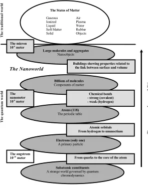
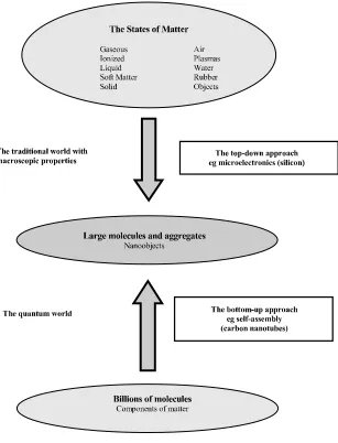
The nanoworld is the intermediary between the atom and the solid, from the large molecule or the small solid object to the strong relationship between surface and volume. Strictly speaking, the nanoworld has existed for a long time and it is up to chemists to study the structures and properties of molecules. They have learnt (with the help of physicists) to manipulate them and build more and more complex structures. Progress in observation tools (electron microscopes, scanning-tunneling microscopes and atomic force microscopes) as well as in analysis tools (particularly X-ray, neutron and mass spectometry) has been a decisive factor. The production of nanoscopic material is constantly improving, as is the case for the process of catalysis and surfaces used in the nanoworld. A substantial number of new materials with nano elements such as ceramics, glass, polymers and fibers are making their way onto the market and are present in all shapes and forms in everyday life, from washing machines to architecture.
Large molecules and aggregates
Nanoobjects
The States of Matter
Gaseous Air Ionized Plasma Liquid Water Soft Matter Rubber Solid Objects
Billions of molecules
Components of matter
Atoms (118)
The periodic table
Electrons (only one)
A primary particle
Subatomic constituents
A strange world governed by quantum chromodynamics
The micron 10-6meter
The angstrom 10-10meter
The quan tum w or ld Th e tr ad it io n al wo rl d The Nanoworld The nanometer 10-9meter
T h e em er gen ce of n ew p os si b ilities Atomic orbitals From hydrogen to ununoctium
From quarks to the core of the atom Chemical bonds - strong (covalent) - weak (hydrogen) Buildings showing properties related to
the link between surface and volume
Biology has been molecular for a long time. The areas of DNA, proteins, and cellular machinery are all subjects of multidisciplinary research. Investigations into these fields have been carried out by biologists, chemists, and physicists. Furthermore, the tools that have been developed have created new areas of specialization, such as bioinformatics. Observation, image-processing and simulation all benefit from the advances in information technology and, once more, conceptual progress goes hand in hand with technical expertise.
The concept of the nanoworld is based on the convergence of a real mix of scientific and technological domains which once were separate.
Even though the laws of quantum mechanics based on wave corpuscle duality are not directly visible in our everyday world, except for lasers and semi-conductor components, they do govern the nanoworld. In the future, the quantum effects will be used in a large number of applications, and in objects with new properties, such as quantum cryptography, quantum computers, teletransportation, etc.
The evolution of our know-how, and of technological innovations, is already having significant consequences. The Internet is the fruit of the union between information technology and telecommunications, just as biochips are for electronics and biology. Imaging on a molecular level revolutionized the techniques of medical examinations. The borders between chemistry, physics, mechanics and biology are disappearing with the emergence of new materials, such as intelligent systems, nanomachines, etc.
1.2. References
1.2.1. Two basic facts
The evolution of knowledge
This is a fabulous adventure where the frontier between fundamental science and applied science becomes an area of exchange and innovation. If the laws of electricity make the electric motor possible, then we can make the same comparison for the electron and television. We are going from the macroscopic to the microscopic.
Technological expertise
Progress in metallurgy and in chemistry has allowed scientists to process silicon. Physicists, in particular, have highlighted its semi-conductor properties. The understanding of these allowed the invention and the production of the transistor. A long succession of successful discoveries and innovations has meant that integrated circuits are now present in everyday objects. If an object can be understood in detail at the microscopic level, we can use our knowledge to apply it to the macroscopic level.
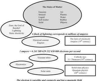
The electron
A primary particle
The States of Matter
Gaseous Air Ionized Plasma Liquid Water Soft matter Rubber Solid Objects
Large molecules and aggregates
Nanoobjects Zeus, the God of
thunder! Lightning Static electricity Electrical current Engines Vacuum tubes Electronics Microelectronics Solar units The scanning-tunneling microscope
A flash of lightning corresponds to millions of amperes
1 ampere = 6 241 509 629 152 650 000 electrons per second
The laws of electricity Ampère (19thcentury)
Cathode rays J.J. Thomson (19thcentury)
Solid-state physics Quantum physics (20thcentury)
The electron is wavelike and corpuscle and has a magnetic field
Spintronics
Figure 1.2.The scientific approach is advancing on all fronts: from lightning to the electron, from the thunder of Zeus
1.2.2. Two approaches
It seems that the level of knowledge and technical know-how has never been as advanced. This in turn allows for the manufacture of intelligent objects which result from the merging of two approaches:
– top-down, which enables us to control the manufacture of smaller, more complex objects, as illustrated by micro and nanoelectronics;
– bottom-up, which enables us to control the manufacture of atoms and molecules, as illustrated by supramolecular chemistry.
The traditional world has come together with the quantum world. Sectors that were once separate are now coming together. The natural world is of interest to physicists as well as to computer scientists and mathematicians. The divisions between the different disciplines are disappearing and paving the way for new paradigms.
1.2.3. Two key points
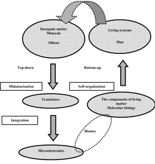
Miniaturization
This process makes it possible to see, work on and manufacture ever smaller objects. In order to do so, increasingly sophisticated technology is required.
Complexity
Bottom-up
The components of living matter Molecular biology Inorganic matter
Minerals Silicon
Top-down
Microelectronics Transistors
Living systems
Man
Self-organization
Integration
Bionics Miniaturization
Figure 1.4.Two key points: miniaturization and complexity. Self-organization in the bottom-up approach (eg living systems),
1.3. Some bonus material for economists
Recent government measures aim to discover what impacts these new technologies will have on the economy. These measures bring considerable investment in developed countries: the global effort was US$10 billion in 2004 and this was double the figure from 2003. Large American companies, such as IBM, HP and 3M, invest about one-third of their research and development budget in nanotechnologies. There are more than 1,000 start-ups that have declared that they are carrying out research in the area of nanos.
However, these figures should not to be taken as definitive since they depend on the generally restrictive definition that is given to the area of nanotechnology. Nanotechnologies often share some common ground with microtechnologies from which they are partly derived. Strictly speaking, nanotechnologies do not include technologies measuring up to several tens microns in size, at least not at present. This is frequently the case for MEMS (Micro Electro Mechanical Systems). Furthermore, an ambiguous common ground, if one exists, divides traditional chemistry from modern chemistry in the area of molecular auto-binding, the aim of which is to lead to self-organized materials and systems.
Miniaturization and complexity
What do the development of cells and organisms have in common with the day-to-day running of a town or society? The answer is complexity. Complexity, under different variants, is present everywhere in the nanoworld. With regard to products originating from the top-down approach, except when used industrially (when referring to complex industrial systems), it seems that true complexity lies in software or, in other words, in the intelligent objects themselves. The duplication of millions of identical elements, as well as the links between them, admittedly leads to complications. However, complexity can be found in both self-repair and self-learning programs. Thus, hierarchical organization defined in terms of components, machines and systems is moving ever closer to the organization we see in biological systems. In the technology of the future, the recognition of error management and of corrections will reinforce this analogy.
Complexity is a notion that brings unpredictability into play. If biosystems are strongly hierarchical in terms of their level, ie molecules, cells, organisms, and populations, then these four systems are, unlike computers, interdependent. Complexity comes from unpredictable emerging functions in the bottom-up approach. These functions not only provide organisms with the sturdiness they need in order to live, but also create opportunities for evolutionary adaptation depending on the external conditions. It is this concept that is being discovered in new emerging phenomena, which is, of course, understandable, but at the same time is occasionally unpredictable. For example, the multiplicity of interaction loops makes their analysis with genes extremely difficult. Remember that each protein has its own gene code, meaning that each gene determines the chain of a certain number of amino acids. This is only the beginning of understanding how molecular machinery works.
Chapter 2
The laws of quantum physics give a universal image of our world. These laws are essential to our understanding of the nanoworld. The laws of traditional physics describe
2.1. Quantum physics
2.1.1. From the traditional world to the quantum world
The nanoworld is part of our world, but in order to understand this, concepts other than the normal ones, such as force, speed, weight, etc., must be taken into consideration.
The nanoworld is subject to the laws of quantum physics, yet evolution has conditioned us to adapt to this ever changing world. This observation has led us to further investigate theories based on the laws of physics that deal with macroscopic phenomena.
Therefore, the law linking the pressure of a gas “P”, its volume “V” and its temperature “T”, following the equation P u V/T = a constant, is one of astounding simplicity. It describes how engines work. Each liter of gas, at atmospheric pressure, contains approximately 10,000 billion billion atoms, and because of this immense size we are unable to predict the individual movement of the atoms. This movement can only be observed in exceptional vacuum conditions and in exceptionally low temperatures, but the laws of physics that are applied will no longer be the same.
of physics will no longer be the same. If the notion of electric current is intuitive and does not create any problems of representation, such as fluid analogies, then the electrons in the final component state will not be the same.
Furthermore, in the macroworld, sizes are continuous; however this is not the case in the nanoworld. When we investigate and try to understand what is happening on this scale, we have to, strictly speaking, change the way we look at things. New concepts of quantum physics can only come directly from our surroundings. However, our world is fundamentally quantum. Our common sense in this world has no value in the nanoworld; we have to invent new concepts. This does not happen overnight: little by little, scientists have been able to interpret all known phenomena and give them a joint, common theory which has never been called into question.
This is recent history. In fact, we had to wait for the 20th century and the observation of the atomic world to reach the real limits of traditional physics and create a new branch of physics, quantum physics.
Until now, no observation has proved the theories of quantum physics wrong and it remains an area that is still under investigation.
Quantum physics also describes an extraordinary world with entirely new properties that are difficult to imagine, but which give us a better understanding of chemistry, transistors and lasers.
2.1.2. Two fundamental concepts
2.1.2.1. Wave-corpuscle duality
Particles can behave like waves. This property, particularly for electrons, is used in different investigative instruments in the atomic scale:
– The scanning-tunneling microscope, which lets us look at atoms on the surface of a lattice, uses an effect of quantum physics, the tunneling effect, which allows particles to pass through a barrier.
– The electronic microscope whose function is based on the wave properties of electrons, and whose wavelength and speed both correspond to light with a very short wavelength.
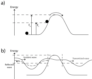
Figure 2.1. An effect of quantum physics: the tunneling effect
a) The passage of a particle through a barrier in the traditional world: the particle does not pass if Ec < Ep and the particle passes if Ec > Ep.
b) The passage of a particle through a barrier in the quantum world: the probability of passage is not zero when Ec < Ep and the probability increases
2.1.2.2. Probability in the quantum world
Quantum physics gives a completely different version of the world on the nanometric scale than that given by traditional physics. A molecule is described by a cloud of probability with the presence of electrons at discrete energy levels; this can only be represented as a simulation.
All measurable sizes are subject to the laws of quantum physics which condition every organism in our world, from the atom to the different states of matter.
The nanoworld must therefore be addressed with quantum concepts.
Chemistry is quantum.
The chemistry of living organisms is quantum.
Is the functioning of our brain closer to the concept of a quantum computer or to the most sophisticated microprocessors?
All properties of matter are explicable only by quantum physics. Traditional physics, which is certainly efficient and sufficient in the macroscopic domain, only deals with large objects (remember that there are nearly 1023 atoms per cm3 in a solid), while quantum physics only deals with small discrete objects. However, the evolution of techniques and the use of larger and larger objects stemming from scientific discoveries make us aware of the quantum nature of our world in all its domains. Our vision of this has been completely transformed, and our lives have been changed as a result.
Just as Alice did in Alice in Wonderland, we are going to have a look at things from the reverse side. Before leaping into the submicronic world we need to understand some of the key ideas that await us there.
2.2. The key players
2.2.1. The electron
2.2.1.1. The cornerstone of matter
Everything starts with the atom, the building block of the nanoworld, and also of our world. Mass is predominantly concentrated in the nucleus of the atom, which is made up of particles called protons which have a positive electric charge, and of neutrons which are neutral, but which have the same mass as protons. The neutrons stabilize the confinement of the protons which are subject to their mutual electrostatic repulsion. This nucleus is packed with negatively charged particles called electrons which are equal in number to the number of protons. The atomic unit is therefore neutral. It is the distribution of electrons that is the origin of the atom’s chemical properties.
2.2.1.2. Electronic states
It is clear that for the atom, things start to become more complicated.
Electrons occupy discrete states, in other words quantum states. In the quantum world, the continuous does not exist and places are numbered. The various different states are predefined and are identified by a number.
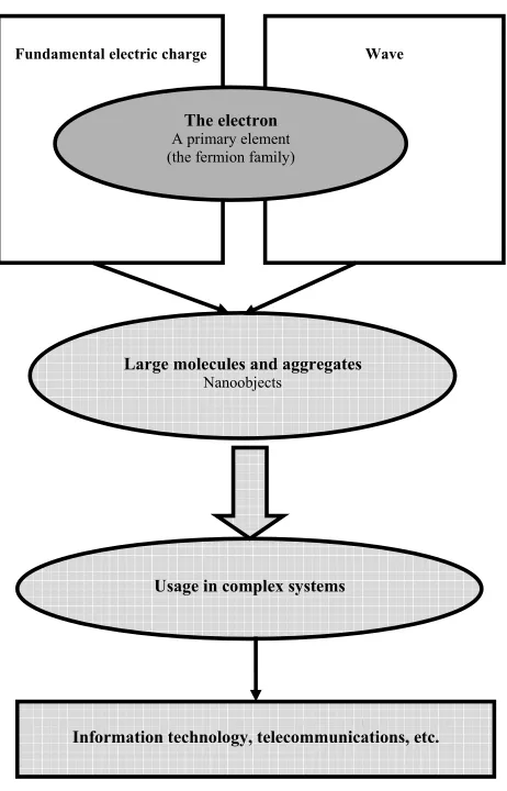
Large molecules and aggregates Nanoobjects
Wave Fundamental electric charge
The electron A primary element (the fermion family)
Usage in complex systems
Information technology, telecommunications, etc.
Two electrons can occupy, at most, one state, which is due to the existence of two spin values1. As we look closer, the atom becomes heavier and the number of electrons increases. They are divided in an orderly fashion around the nucleus, forming concentric shells starting with the one closest to the nucleus, just as you would fill up a theater from the front row to the back. Each shell has a limited number of states. The most important shell for interactions between atoms is the outer shell which has four states, meaning that there is enough space for eight electrons, except for hydrogen and helium. This has fundamental consequences.
The ranking of atoms by their mass in relation to their chemical properties highlights this periodicity; in other words Mendeleev’s periodic table of elements. Thus, when there is only one electron on the external shell we are dealing with alkali metals, such as lithium, sodium, potassium, and rubidium, all of which come from the first column of the periodic table. When the outer shell is full, meaning that when there are eight electrons on the shell, we are then dealing with the noble gases, such as helium, neon, and argon, which make up the eighth column of the periodic table. Hydrogen, which has one proton and one electron, plays a key role in molecular construction and in our world in general. Its external configuration determines other chemical properties.
2.2.1.3. The quantification of energy
A key idea in the atomic world is that of quantification. As no two states are the same, every exchange that occurs between them must be carried out through “packets” of energy, each with a
defined value which corresponds to the energy difference between them. In the atomic world, every process must be carried out step by step; there are no short cuts. It is still possible for an electron to be excited if it receives enough energy to progress to a superior level, if one is available and not already occupied. This energy can be supplied by a shock, in particular by light stimulation. It is the process of atomic absorption which lets us probe the atoms in order to find out more about their different states. The reverse occurs if we remove an electron from one of the outer shells. In this case, there will be a knock-on effect leading to the source of the light. The balance that is reached always corresponds to a minimum level of energy.
All of these properties are used in nanometric objects.
2.2.1.4. Bonds
Thanks to their surface electrons, atoms form more complex edifices: molecules or solids which create new properties. The fixing between atoms is known as chemical bonding.
The concept of bonding is as old as that of the atom. Its most famous interpretation comes from the Greek philosopher Democritus who saw that the bonding between atoms was a property linked to their shape, smoothness, and ability to lock onto other atoms. Chemical bonding can only really be explained with the knowledge of the quantum nature of the electron.
molecules. A good example is given by stacking pieces of Lego together in order to create larger complete structures. The bonding force for atoms is based on the fact that the energy from the state created by the two shared electrons is weaker than the two independent states. More precisely, while the atoms approach one another, the atomic states taking part in the covalent bond will form two molecular states, one of which is bonding and the other, with a superior energy level, is anti-bonding. Each state accepts two electrons of opposing spin; the bonding molecule is full and the other anti-bonding one is empty.
Physicists talk about molecular orbitals, often represented in chemical formulae by a line, for example the C-C bond between two carbon atoms. This idea of a molecular orbital is very useful for visualizing the bonds between atoms. This is the most solid bond in chemistry, the universal adhesive which forms the basis of semi-conductor materials such as molecules of living organisms.
2.2.2. The photon
2.2.2.1. The wave
We live in a world of photons made up of the electromagnetic spectrum which goes from radio waves to X-rays and then gamma rays. We have a very limited perception of the electromagnetic spectrum; visible light is the only part of the spectrum that is directly captured by the eye. Our body perceives infrared rays in the form of heat through sensors in our skin and reacts to ultraviolet rays by tanning and sunburning as well as, unfortunately, developing skin cancers.
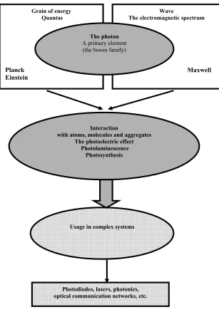
Interaction
with atoms, molecules and aggregates The photoelectric effect
Photoluminescence Photosynthesis
Wave
The electromagnetic spectrum
Maxwell
Grain of energy Quantas
Planck Einstein
The photon
A primary element (the boson family)
Usage in complex systems
Photodiodes, lasers, photonics, optical communication networks, etc.
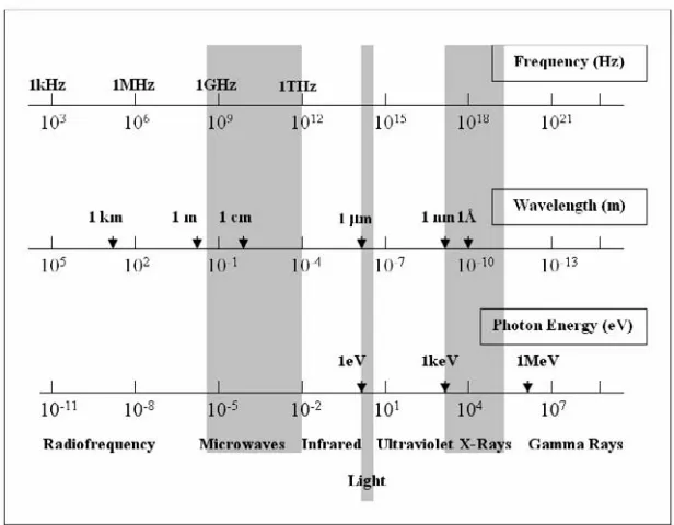
Figure 2.4. The electromagnetic spectrum
Units of abbreviations:
Hz hertz m meter eV electronvolt
THz terahertz Å angstrom MeV mega-electronvolt GHz gigahertz nm nanometer keV kilo-electronvolt MHz megahertz Pm micron
kHz kilohertz cm centimeter
2.2.2.2. The energy grain
However, a small phenomenon has appeared and raised doubt in peoples’ minds and revolutionized our conception of light: the phenomenon is that of the photoelectric effect.
Some time will be spent on this development because it signifies the division between traditional and quantum physics. When a beam of monochrome light is sent onto a solid object, the solid object will only emit electrons from a certain frequency of this light. The interpretation, which was given by the famous physicist Albert Einstein, is that light carries its energy “E” by discrete packets which are proportional to its frequency “Q”: E=hQ! These discrete packets are known as quanta, which give their name to the new area of physics known as quantum physics.
The nature of the photon is, however, very different to that of the electron. First of all, it has zero mass, it travels at a speed that particles with mass cannot even dream of reaching, and it can travel in a group in the same energy state. Therefore, photons can be stacked together in any number in the same space. This last property is the basis of the laser effect: a laser beam is in fact made up of photons of the same type, meaning the same energy.
Physicists talk about different families; remember that the electron belongs to the fermion family and the photon belongs to the boson family. We, as humans, are closer to the fermion family!
Let us come back to the photoelectric effect. We know that the energy of electrons varies under a discontinuous form, or to be precise, it occupies specific predefined states of energy.
In order to change state, in this case moving from one energy level in a specific material to an energy level in a vacuum, a single grain of energy is required. This corresponds to the difference in level from where the threshold (the minimum level of energy required in order to pass to the next level) appears. Generally, all interactions between electrons and photons are quantified, thus giving rise to the phenomenon of luminescence that can be seen in the nanoworld, particularly in the area of imagery.
The quantum nature of the photon is used in a spectacular way in protecting confidential information.
In order to ensure communication security, man has always invented very elaborate coding systems; this is known as cryptography. Unfortunately, because of the power of calculation in modern computers, the codes always end up being cracked due to the fact that they are primarily based on arithmetic. This is especially evident in the world of banking where there is always a need for more sophisticated coding.
With photons, a new type of cryptography is starting to appear, especially in state-of-the-art laboratories which have very sophisticated instruments; this is known as quantum cryptography. This is based on the absolute ban on reproduction, which means that it is impossible to copy information. In the quantum world, measuring devices change the quantity of the measured object, so, if we measure a given state of a photon, we then transform it. It is like a locksmith who sees the lock change every time he tries to put the key in it.
This new method is imperative as it is the definitive weapon against theft.
a)
b)
Figure 2.5.The photoelectric effect
a) Experience. While the surface of a metal vacuum is illuminated with monochrome light, the surface will emit electrons if its frequency Q is more than a certain value Qg.
b) Physics. Light is made up of energy photons E = hQ While E < Eg (Eg
2.3. Molecules
From atoms to molecular self-assembly, we are witnessing the continual emergence of new properties.
The most complex edifices, ie molecules, are organized by the grouping together of atoms. It is the properties of these molecules that give us the world in which we evolve.
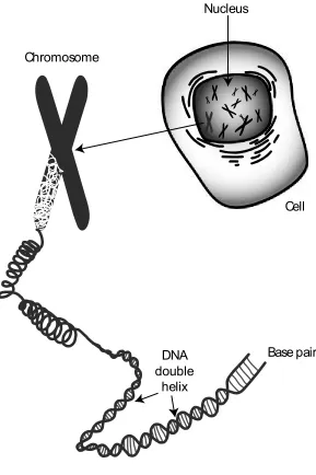
In fact, the grouping of atoms reveals the notion of functionality; from acid carrying hydrogen with one atom, up to large molecules in living organisms, genes and long chains of molecules assembled in a helix. The latter carries the building blocks of living organisms2 which are not only present in the nanoworld but also in our world.
2.3.1. From the smallest molecule to the largest and their spectacular
properties
The water molecule: H2O
The extraordinary subtlety of the hydrogen bond means that humanity is unable to work out the different characteristics of its phases; for example, a liquid which solidifies itself into an ice crystal is less dense than water. Water is necessary for life on earth. Another example is a solid snow structure whose infinite complexity allows researchers to carry out up-to-date research in order to optimize the friction coefficient. We are witnessing the emergence of new properties which are replacing those of their
atomic components. This will be the same for structures with an increasing complexity.
Proteins
These molecules, which have enormous edifices with multiple configurations and functions, have developed a soft chemical catalyst by using the lock and key effect to interact. Here, an atom has its own unique place: carbon, which has four electrons in its outer shell (a half-full shell), is at the heart of the chemistry of living things along with hydrogen, oxygen, nitrogen, and some other elements. The atom is at the origin of the extraordinary variety of proteins which replicate themselves, join together, construct and deconstruct.
Carbon nanotubes
These new objects, which are between the size of a molecule and an aggregate, will perhaps replace silicon which is the current leader in the world of electronics.
2.3.2. Functionality
However, simulation, which is an extremely powerful approach based on the use of computers with advanced calculating capabilities and on the possibilities of unlimited information storage, has come to our rescue. This will be discussed later in this chapter.
2.4. Solid matter
After molecules, another important construction is that of solid bodies, some of which have a particular status in the nanoworld. How can we consider an atomic aggregate of several nanometers in diameter to be an insulator or conductor with the magnetic and electrical properties according to size? First of all, we need to understand the behavior of the electron in solids when affected by external factors which is the case for crystalline bodies. After this, we will be able to analyze the effect of the size of the aggregates.
Whether the solid is an insulator, conductor or semi-conductor, everything depends on the circulation of electrons within it.
2.4.1. Insulators or conductors
The fact that a body is an insulator or a conductor is only the consequence of the electron’s ability to move.
case of glass (silicon oxide) or diamonds (covalent crystal of carbon).
On the other hand, metal is a conducting material. Its properties can be described in a relatively simple way by considering it as a “box” with free electrons. This “box” is made up of atoms of ionized metal that are positively charged. The resistance characterizes the shocks of the electrons with the ions, which increases with thermal agitation and therefore the temperature. Knowing that there is one electron for one ion, the density of electrons is very large and therefore the current is important. In the case of aggregates, where the number of atoms and therefore electrons is reduced, we start to notice the individual behavior of the electrons, for example in surface interactions which give particular optic properties. Without being fully aware of its properties, ancient glassmakers used gold dust to color glass.
2.4.2. Semi-conductors
One particular item is essential for solid-state electronics and that is semi-conductors. They conduct electricity, but in a weaker way than a metal does. They allow for the manufacturing of components, such as the famous chip.
2.4.2.1. Silicon crystal
Let us then introduce some phosphorus into the silicon crystal in a weak concentration (doping is the term used when referring to semi-conductors). One phosphorus atom per million is a weak doping and one phosphorus atom per thousand is a strong doping. The phosphorus atoms randomly take the place of the silicon atoms without disrupting the crystalline lattice. The silicon crystal now becomes a conductor. Why? The phosphorus atom has five electrons on its outer shell, of which four are used to bond with their four neighboring atoms. The fifth electron is free and is only slightly held back by its original atom whose outer layer has eight electrons and is therefore saturated. It can consequently move within the crystal. We talk about n-type conduction (n for negative) and n-type silicon where the current is electronic.
a)
Figure 2.6.Molecular orbitals and the band structure of crystalline silicon
a) The chemical bond between two atoms is due to the joining of two electrons on a molecular orbital created by the interaction. The orbital possesses two energy levels, bonding and anti-bonding, separated by an energy '(In a solid, these levels widen to become bands, the valence band (VB) and the conduction band (CB) respectively.
b) For silicon (Si) which has four electrons on its outer shell, each electron bonds with one of the four neighboring atoms in the crystal. All the electrons take part in the bonding process. Thus, the valence band is full and there is no possible displacement of charge.
If a silicon atom is replaced by an atom from column 5 of the periodic table, such as arsenic (As), the fifth electron is weakly bonded and passes to the conduction band. The silicon crystal becomes a n-type conductor. If a silicon atom is replaced by an atom from column 3, there is an electron missing. This creates a hole which lets an electron move into the valence band. The silicon crystal becomes a p-type conductor.
2.4.2.2. Electrons and holes
A simple representation of the concept of hole conduction can be created with the following analogy. We are driving on a road and if there are not many of people on the road then it is not difficult to get from one place to another; there is enough space for everyone. If there is a lot of traffic, our movement is then dependent on the number of available spaces. This image lets us understand the idea of hole conduction.
If we observe a large crowd of people, where one free place in the crowd allows gradual movement, movement appears to occur as if the “holes” travel in the opposite direction of the people who use them in order to move forward, as is the case for bubbles that rise in a liquid and represent the displacement towards the bottom of the corresponding liquid.
2.4.2.3. Junctions
isolate themselves, which is a property used in semi-conductor components.
On the basis of these components, technology lets us engrave billions of microscopic transistors together on the same plate, which when appropriately organized helps us create microprocessors.
2.4.3. Nanomaterials
As is the case with metals, we can produce structures with one, two or three nanometric dimensions. The most common structures are thin layers whose different production techniques enable us to precisely control the depth of the layer, measured in nanometers. Two examples include the self-cleaning surfaces of spectacles (the lotus effect) and silver bactericidal nanocatalysts in certain washing machines.
On this level, purely quantum effects will arise. We are talking about metamaterials, quantum wells, and other remarkable objects which are fascinating scientists, and becoming more and more a part of our daily life.
2.5. Quantum boxes: between the atom and the crystal
pseudo atoms under excitation, can be adjusted in the visible domain. This technique is largely used in the medical world where nanocrystals are used as fluorescent markers. We find a similar explanation for quantum well lasers.
2.6. Some bonus material for physicists
Let us now address the laser effect. What does laser mean? Laser stands for Light Amplification by Stimulated Emission of Radiation.
A laser is a common, visible object: from blackboard pointers to disco lights, we recognize lasers because they have a perfectly defined color – they are monochrome – and because the beams are straight. Their rays diverge much less than a normal projector.
The qualities mentioned above are linked because we use the properties of a cavity3 in order to amplify and monochromatize the light. This light is normally emitted spontaneously from certain materials by the fundamental process of luminescence.
2.6.1. Luminescence
We have seen that electrons in an atom occupy a clearly defined state of energy. In their basic state, they occupy the electronic state with the lowest energy. If we put an electron into a superior electronic state, it becomes excited. Very quickly it will become de-excited by emitting energy.
In an atom, the energy exchanges are carried out by photons. Excitation and de-excitation correspond to the absorption and emission of a photon respectively during energy exchanges between two different energy states. The emission is completed either spontaneously or by stimulation by the photons themselves following an entrainment process. There cannot be any amplification in this case since the more the atom becomes excited, the more it will become de-excited. At most, we have a balance between the atoms in their basic state and in their excited state.
Let us now consider a system with three states of energy: the basic electronic state F and two excited electronic states with superior energy, E1 and E2, with E2 having more energy than E1. We excite an electron so that it can pass into the E2 state. It comes back to its basic state by either directly emitting a photon of the same energy as what it has absorbed, or “in cascade”, by passing through the intermediary level E1. In the second case, it emits two photons whose additional energy corresponds to the unique energy of the direct transition. The excited electron has the choice between these two mechanisms. If the transit via the intermediary level E1 is the quickest path, then it is clear that this is the path that will be taken by the electron.
This is what happens to certain atoms when they are introduced into solid bodies. The first, most commonly known example is chromium when it is introduced into an alumina lattice, which gives us rubies. It absorbs green light (transition A: from the basic state F to the superior excited state E2) and emits red light (transition E: from the intermediary state E1 to the basic state F).
Furthermore, the transition towards the E1 level is a lot faster than the direct transition to the basic state, and is carried out by a non-radiation process producing heat.
This technique is essential because we have the possibility, by using green light, of having more atoms in the excited state than in the basic state during the lifetime of the E1 state, which is not subject to the absorbed protons by the E2 state. This phenomenon is known as population inversion. An amplification of light in this case is possible: for red light, the absorption is weaker than the stimulated emission that it will lead to, thus the laser effect is attained.
2.6.2. The laser device
If the amplifying medium is placed between two parallel mirrors forming a resonant cavity, then the red light will spontaneously release itself by auto-stimulation. The coherent stimulated amplification is then made by following a type of resonance which creates a very monochrome and guided beam of light following the axis of the cavity; the cavity being the mirror which is slightly transparent. We now have the laser effect.
Many other materials that possess light-emitting centers are used to create lasers of different wavelengths. If we continue the permanent excitation of atoms, or optical pumping, we have continuous wave lasers. If the excitation comes from a flash source, then we have a pulse laser.
same techniques that are used in microelectronics. Thus, at present we are able to develop hybrid circuits integrating lasers on silicon circuits, mainly for use in the world of telecommunications.
Figure 2.7.Light-emitting diodes and lasers: general principles
a) The electron of a light-emitting source, for example the ion Cr+3, in the
aluminum matrix for a ruby laser is excited from its basic structure F up to a state of energy E2 width 'E (absorption band). It quickly passes to the discrete state E1 by losing its energy in a non-radiative way.
B.C. c) C.B. V.B. hQ Energy F.B. x Speed Energy hQ V.B. d) C.B. e) Energy x p n
hQ f) x Energy F.B. Electrons Holes C.B. F.B. V.B. C.B.
AlGaAs AlGaAs GaAs
hQ
Figure 2.8. Semi-conductor lasers
c) Diagram of a band. The valence band (VB), the forbidden band (FB) and the conduction band (CB). An electron is excited and passes into the conduction band. It immediately relaxes with the minimum energy of the conduction band. Furthermore, the hole that it leaves relaxes at the top of the valence band, otherwise known as the minimum energy principle, which is always used by electrons. The electron comes back to its basic state by emitting a photon of energy hv.
GaAs (Gallium Arsenide). We say that the semi-conductor is a direct gap semi-conductor4.
e) Representation of the emission technique in a “pn” junction. Strictly speaking, electrical excitation takes place in a direct polarized junction by the introduction of carriers: electrons from the conduction band “n” recombine at the junction with the holes from the valence band “p”. By altering the make up of composite compounds, we can adjust the emitting wavelength by changing the width of the forbidden band. A multitude of different types of more or less sophisticated light emitting diodes (LEDs) are produced using this technology. When the structure of the diode is a Perrot-Fabry cavity we have a laser diode.
f) Quantum wells. These are created with compatible materials from different forbidden bands. When the thickness of the shell is nanometers deep and the shell is sandwiched between the shells of more important forbidden bands (example: AlGaAs/GaAs/AlGaAs) then we see atomic pseudo-states starting to appear just as in quantum boxes, giving rise to a new type of quantum optoelectronics.
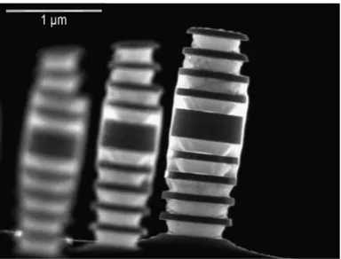
Figure 2.9. Quantum dot for single photon experiments: 400-nm-diam micropillar, produced by e-beam lithography and reactive ion etching from a
GaAs/AlAs-layered planar structure grown by molecular-beam epitaxy
The theory of symmetry groups
From the atom, and indeed from the subatomic to the solid, the theory of symmetry groups gives a powerful definition of the above listed areas of science and can be easily adapted to the quantum world.
It is based on operator algebra. For example, the “rotation” operator (R) enables us to rotate a body. If the body is of spherical symmetry any type of rotation transforms the body in itself. The particular states of this operator5 are
well known mathematically; they are known as spherical harmonics.
As far as the atom is concerned, its electrons occupy defined states of symmetry using the coulomb potential. The operator that lets us calculate the energy of the states is known as the Hamiltonian (H). It is clear that the energy from the atom is independent of any geometric rotation that we can subject it to, which translates mathematically by the fact that the operators R and H can switch places with one another. This means that we can apply the two operators in one state in any order so that RH = HR for the same result.
In operator algebra, an important theory states that when two operators commute they have the same basic functions. The particular states of the rotation operator therefore create a basis for the quantum states of the atom, which in turn explain the distribution into successive layers and all the quantum numbers of the electronic states. This is truly amazing.
In a periodic solid, the application of the “conservation law of momentum” from the electron to the operator of translation gives the functional shape of the quantum state waves, the famous Bloch functions and band theories. We cannot really say anything more; all we can do is admire a theory based on a fundamental concept, that of symmetry. When theory becomes a work of art it almost resembles poetry: “There’ll be nothing but beauty, wealth, pleasure, with all things in order and measure”6.
Chapter 3
The eye
(1/10 mm)
The optical microscope
(The micron: 1/1,000 mm)
The electronic microscope
(The nanometer: 1/1,000 m) X-ray crystallography
Nuclear magnetic resonance (NMR) Fluorescence spectroscopy
The atomic force microscope Observation
The quantum world
Observation is at the origin of all scientific discoveries.
The nanoworld is becoming more important and is even becoming an area of scientific discovery thanks to the progress that has been made in the techniques of observation.
3.1. Observing with photons
3.1.1. The optical microscope in visible light
The optical microscope was the first instrument that enabled man to observe objects normally invisible to the naked eye. As the microscope is subject to the laws of optics, its resolution is limited to several tenths of a micron. In order to study samples from living organisms, the samples must be prepared with coloration techniques.
A new generation of microscope which uses laser light appeared in the 1980s. It has enabled scientists to create three-dimensional images at different levels of depth of the matter being studied by using focalization and laser beam scanning. This type of microscope is known as a confocal microscope1 and is particularly adapted for use in the natural world.
One very interesting use of these microscopes corresponds to their ability to work with fluorescent markers. The laser beam excites a fluorescent substance which has been added to the sample, for which we know the affinity for certain molecular sites. Thanks to these markers we can, for example, selectively view certain reactions. The fluorescent signals are detected by electronic
sensors and these signals are then amplified. The image is then processed by computer.
3.1.2. X-ray machines
X-rays are photons with a wavelength that is much shorter than the wavelength of ultraviolet light. X-rays are produced from an accelerated shock of electrons against a metallic target.
One of the first applications of machines using X-rays was in the macroscopic domain. The X-rays benefit from the fact that this radiation has a strong penetrating power in materials with the rate of absorption depending on the density of the material. Radiation transmitted through a body coated with a phosphorescent or photosensitive substance is commonly known as radio waves. A sophisticated version of this type of machine is the X-ray scanner. The transmitter turns around the object at the same time as the receptor does, measuring the intensity of the X-rays transmitted. The data is processed by a computer which reconstructs cross-sections of the object, in other words 3-D imagery. The resolution is determined by the quality of the X-ray beam used. This type of machine is used in many applications, especially in medical imagery.
analysis is possible, firstly, due to the quality of today’s machines and, secondly, because of the sophisticated calculation techniques used. This type of machine is an essential tool for chemists who want to assemble molecules in crystalline form in order to study their atomic pattern. This method enabled the discovery of the double helix by Francis Crick and James Watson in 19532.
3.2. Observing with electrons
Electron microscopy uses the wave properties of electrons. However, as particles they need a vacuum in order to travel. Microscopes are in the form of a metal vacuum enclosure in which the following can be found:
– The electron gun, such as in cathode ray tubes used in television sets.
– The different elements of electronic optics, such as electromagnetic lenses (equivalent to traditional optic lenses) which control the trajectories of the electrons as well as the support of the object to be studied.
There are two types of electron microscope.
3.2.1. The transmission electron microscope (TEM)
In this type of microscope, as with X-rays, the beam interacts with the crystalline sample and creates a diffraction figure, or hologram. The analysis of the diffraction figure enables us to study the atomic structure of the sample being analyzed. The final resolution is related to the associated wavelength of the electrons
and therefore to their energy. The most powerful machines work with voltages in the region of hundreds of thousands of volts.
3.2.2. The scanning electron microscope (SEM)
The surface of the sample under study is scanned with an electron beam. The size of the scanned surface depends on the level of enlargement desired. The interaction between the electrons and the sample gives rise to different signals (the emission of electrons and photons) which when gathered and analyzed bring together the image of the surface of the observed sample without using any mathematical process, contrary to the process of the TEM.
The resolution of this type of instrument, limited by the machine’s technology, enables scientists to view objects at an atomic scale (1/10 of a nanometer).
A significant restriction of this microscope, as is the case for the TEM, is that it needs a vacuum. The samples need to be prepared in a specific manner, in other words they need to be plated, cooled, and cut into thin sections, all of which are clearly impossible when observing living organisms.
Figure 3.1.The environmental scanning electron microscope: a) a general view of the environmental scanning electron microscope,
b) example: detailed makeup of the eye of a drosophila
a
3.3. Touching the atoms
The atomic microscope is mainly used in research laboratories. It works on a simple principle, but with very sophisticated technology.
Scientists create an image of vertical displacement from a point on the surface of a sample. This point is made up of some atoms (eg thinned down tungsten microcrystal atoms) and the precision of displacement is to the nearest 1/10 of a nanometer.
In the first version invented by IBM researchers3 in 1981, the control signal is the current, albeit extremely weak, existing between the point of the microscope and the surface of the sample without any contact between the microscope and the sample. However, they are at a distance where the electrons can pass through by using the tunnel effect. In this case, we are referring to the scanning-tunneling microscope.
When there is contact between the point of the microscope and the surface of the sample, the microscope is called an atomic force microscope. This is the nano equivalent of our old gramophones. This type of microscope enables scientists to analyze surfaces with insulating properties, which is impossible with the scanning-tunneling microscope.
An optical version has existed for a short time now, and it is based on the presence of an optical wave that does not move. This evanescent wave is present on the illuminated surface of a sample which can only be detected on a nanoscopic level.
With these instruments, scientists can see the atoms of a surface, but they can also use these instruments to move the atoms, form