_____________________________________________________________________________________________________
Pick and Place Process Optimization for Thin
Semiconductor Packages
Rennier S. Rodriguez
1and Frederick Ray I. Gomez
1*1STMicroelectronics, Inc., Calamba City, Laguna, 4027, Philippines.
Authors’ contributions
This work was carried out in collaboration amongst both authors. Both authors read, reviewed, and approved the final manuscript.
Article Information
DOI: 10.9734/JERR/2019/v4i216897 Editor(s): (1) Dr. Heba Abdallah Mohamed Abdallah,Department of Chemical Engineering, National Research Centre, Egypt. Reviewers: (1) Ayush Dogra, Panjab University, India. (2) Snehadri B. Ota, Institute of Physics, India. Complete Peer review History:http://www.sdiarticle3.com/review-history/47696
Received 30 December 2018 Accepted 04 March 2019 Published 14 March 2019
ABSTRACT
Nowadays, electronic manufacturers trend are to become thinner and thinner especially those electronic gadgets that is very handy and convenient on our daily necessity. Challenge with the leading manufacturers is the production and development of less size gadget yet with richness of available application and uses that we can work on with what can please its consumer for their convenience and satisfaction. As with the semiconductor company, correlation between becoming thinner versus manufacturing capability become significantly opposite, as the package become thinner the more complex its related process can be. This study covers innovative approach in die attach station on critical handling of thin die packages. Lessons and learning were documented from Ball Grid Array (BGA) packages as first to be evaluated with thin package requirements. Also discussed herewith are documented defects and related issues during trials and die attach builds that has been a show stopper on its early production.
Rodriguez and Gomez; JERR, 4(2): 1-9, 2019; Article no.JERR.47696
1. INTRODUCTION
During the early package design reviews, various questions and inquiries were shared with regards to existing die attach machine platforms and capabilities that could satisfy the requirements of the package. Complexity in the package requirements is one great challenge for all team members, motivating to come up with innovative solutions in addressing any issue. Also, one big challenge given is maximizing the available resources to minimize and/or mitigating any possible defects.
Die attach or diebonding is a vital process of any semiconductor Integrated Circuit (IC) manufacturing plant. It is part of the front-of-line operation in which a processing error can convert a high-priced wafer into thousand pieces of expensive scrap [1,2,3]. On the initial evaluation of the project, die crack issue is evident during separation of die to tape and is the top contributor in the Pareto of defects. During the qualification review, it was found that standard pick and place was not efficient in producing good response in terms of die crack. Deriving on risk assessment and planning based on early results to technical judgment in coming up with a selection of all the factors that have major effect. This technical paper discusses how the challenges were turned into milestones wherein issues were addressed by in-depth engineering analysis and utilizing statistical tools at the qualification and optimization.
1.1 Project Statement
These presentation focuses on understanding the cause and main contributor of die crack
defect at die attach stations. Comparison of standard pick and place versus improved pick sequence. Analyzing the behavior of defect and provision of innovative solution and improvement on existing machine capability for a robust processing of thin packages. Documentations of early experience on engineering builds and evaluation for thin packages processing. Assessment on actions and improvement based on the result of table of experiment.
These study covers only early experience on processing of thin die packages based on engineering and line stressing results. Modification of indirect materials and improvement in pick sequence using platforms with “distance to die” setting. Presentation does not include wafer details. Also, pre-assembly process that the wafer undergone is also not stated within the presentation. The focus only of the presentation covers die attach stations, process setting and improvement on indirect materials.
2. REVIEW OF RELATED LITERATURE
2.1 Standard Pick and Place Sequence and Setup
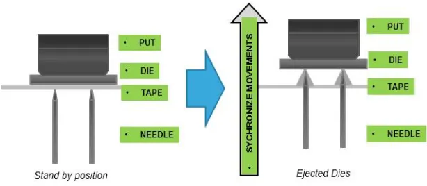
Pick and place sequence of a die attach or diebond machine [4] as illustrated in Fig. 1 emphasizes on the synchronous upward movement of bond head and needle with regards to individually cut die. Individual dice were separated into the wafer tape by the ejection movement of needle against the vacuum hold wafer tape. Different studies in pick and place process are discussed in [5,6,7,8].
For standard pick and place procedure, needle and pick-up tool (PUT) are the primary indirect materials used to pick the individual die from the tape.
Commonly in die attach materials, PUT covers 70-90 percent of the total die size and ejector design configuration with exact outline as compared with the dimension of the die. Furthermore, applicable indirect materials will differ according with the actual die construction and requirements.
For machine set-up procedure, pick and place includes “Teach Z Height” parameter to ensure accurate distance of the PUT to the actual die top surface. These can be performed through recipe “teach” setting, using these procedure machine bond-arm Z travel is computed automatically by the actual reference height distance from die surface to bond-arm standby position.
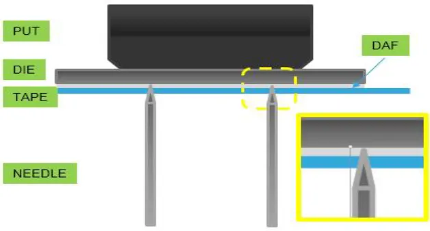
Through a standard pick and place set-up, needle reference height positions are taught on the bottom solid part of the die. Fig. 2 shows the location of the needle underneath the die and tape interface.
In Comparison with die attach films (DAF) packages, needle positioning are beneath the bottom part of the die due to the soft structure of the DAF that during “Z height” learning needle will protrude to the tape and pierced through the DAF since tape has no solid body.
Based on Fig. 3 illustration, DAF package processing needle are located under the die during standby height position.
During ejector wait height position, die are seated above the ejector needles. For standard pick sequence, dies from wafer tapes were separated during eject up movement of the needle together with the supply of vacuum at pepper pot. There is a tendency that the wafer tape are sucked up above the flat surface of the pepper pot and will be hold during needle movement. Simultaneous to vacuum suction, needle will move upward to separate the die from the tape. Dice during needle sequence is supported above by a leveled pick-up tool on top of the die, this is provided with a vacuum to avoid shifting during the picking up sequence. Afterwards, all picked dies will be transferred or placed to lead frame or substrate.
2.2 Indirect Material versus Standard Pick and Place
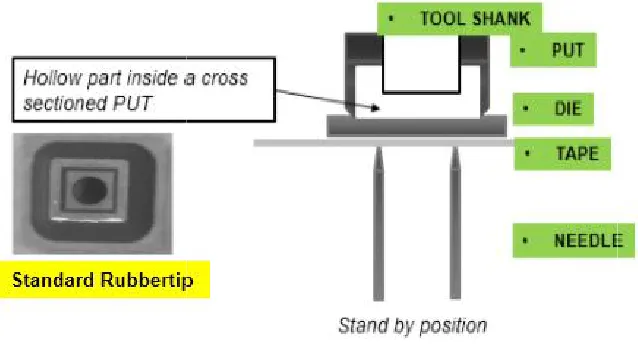
These section explains the relationship of indirect material during pick sequence. Common indirect materials adapted at standard processing is designed having relief or large hollow center portions. These was used to maximize the vacuum needed to hold the die during pick. For die attach process, it is necessary to have enough vacuum too stably hold the die during the movement.
Problem with standard indirect materials and pick sequence as shown in Fig. 4 is observed with high risk for die breakage due to the no equivalent support parallel with the needle location.
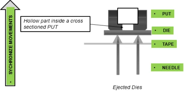
Fig. 5 illustrates fulcrum effect encountered during needle ejection movement due to the bias needle and PUT configuration. The defect manifestation evident at needle location and localization shows cracking in series with needle location both observed vertically on top and bottom part of die.
2.3 Modification in Indirect Materials
By deeply analyzing the defect signature, modification on indirect materials and improving the standard pick sequence has an upright course in providing the innovative solution for thin packages. Changing the current design of the indirect materials needed in processing such pick-up tool including the rubber tip as shown in Fig. 6 from standard design (with relief) to full contact pick-up tool eliminates bias top support versus needle location.
Full contact design ensures parallel support at needle location and pick-up tool, during ejector movement needle will fall on the solid part of the pick-up tool giving upward relief to fulcrum effect during picking process as illustrated in Fig. 7.
Based on the principle of the new design, bending of die which is contributed by the hollow portion from standard PUT design is minimize or eliminated. By these elimination, primarily enhances the facility of the structure of the die at pick position.
2.4 New Pick-up Sequence (Distance to Die)
Rodriguez and Gomez; JERR, 4(2): 1-9, 2019; Article no.JERR.47696
possible deviation at bondhead and needle motors, because of its inherent variation. Position of bondhead and needle can deviate into minimal machine tolerances. This was proven to be detrimental to die since thinning of die made it less resistant to breakage.
In addition, due to the package construction, DAF material is considered for thin packages. Based on the machine response, needle are protruded during “teach Z position”. These shows that die will be seating above the protruded needle during the pick sequence of the machine as shown in Fig. 8. As earlier mentioned, there are minimal deviation on pick z height. To summarize, standard pick and place has high risk in cracking or breakage due to observed possible contributing factors.
By addition of “distance to die” parameter to pick-up sequence results to pick-pick-up tool that will situate above the die without direct contact on the surface. With these, no counter influence during movement of ejector from “stand by” to reference height.
During needle ejection from reference height position, needle will push the die upward
until “distance to die” height will be met. By the result, direct contact of the PUT to die
during pick sequence are eliminated. There will be no collision between die, needle and PUT during pick position. By these responses micro crack possibility during pick can be avoided done by providing enough distance during pick process.
Fig. 2. Position of needle on standard packages
Fig. 4. Cross section of pick
Fig. 5. Cross section of pick-up tool used on standard pick and place (eject
Fig. 6. Standard rubber tip (left), and full contact rubber tip (right) Fig. 4. Cross section of pick-up tool used on standard pick and place
up tool used on standard pick and place (eject-up movements)
Standard rubber tip (left), and full contact rubber tip (right) up tool used on standard pick and place
Rodriguez and Gomez; JERR, 4(2): 1-9, 2019; Article no.JERR.47696
Fig. 7. Cross sectioned area of full contact rubber tip in lined with the needle location
Fig. 8. Pick-up sequence with addition of distance to die
3. EXPERIMENTAL SECTION
The study in Table 1 covers 2 die sizes to be used as test subjects in the study. Both are divided into rectangular and symmetrical type of die. Since the experiment covers thin packages, DAF was used as adhesives in bonding the individual die to substrate.
Initial matrix of Table 2 shows both die sizes to be subjected with different PUT and distance to die parameter.
Three “distance to die parameters” in Table 3 were tested to analyze which of the given selection will result to robust
parameter.
Table 1. Die evaluation
Type of die Die size Adhesive
Rectangular 2.0 x 3.0 mm DAF
Symmetrical 2.5 x 2.5 mm DAF
Table 2. DOE matrix for evaluation
Type of die Die size Pick-up tool Distance to die
Rectangular 2.0 x 3.0 mm Full No
Yes
Symmetrical 2.5 x 2.5 mm Full No
Table 3. Distance to die parameter
Parameter Distance to die
# 1 A
# 2 B
# 3 C
4. RESULTS AND ANALYSIS
All experiment undergone separate legs of experiment in determining the most effective parameter to be set as initial reference. Table 4 shows result of comparison for full contact and standard rubber tip in terms of defects occurrence during pick and place processing.
Based on the table of experiment both symmetrical and rectangular package has an evidence of die crack issue given with no distance to die parameter. But comparing the occurrence of defect results that full contact is better compared with standard rubber tip.
4.1 Design of Experiments
Design of experiments (DOE) includes the occurrence of defect through processing of thin packages, and with the aid of SAS-JMP [9], a system software for statistical analysis. Miss picked and die crack are the main defect measured. These was chosen due to its correlation with the implementation of improvement for indirect material and pick sequence.
Evaluation in Table 5 applies full contact PUT for symmetrical and rectangular dies these is in compliance with the primary result of comparison of indirect materials.
Based on the Table 5, both symmetrical and rectangular dies were tested with three type of “distance to die” parameters. Based on the result Parameter #2 has the best response according with the defect manifestation results and in comparison with different parameters. Both die size of the experiment shows good response that can be achieved during the implementation of parameter #2 in addition with defined PUT configuration. Furthermore, experiment is justified by the tally of defect occurrence. Other pick parameter were not alter during the experiment to avoid noises during the trial.
4.2 Line Stressing Results
During the line stressing and production of larger quantity, Defects are monitored and recorded based on its’ occurrence and tallied with the number of rejected units according with the defect designation. Fig. 9 shows the breakdown of die crack from WK1522-WK1553. Scope includes early line stressing and production for thin packages.
Based on the die crack trend, the average die crack occurrence falls to 20 PPM for the last quarter of the year. Stabilized production improvement was observed during wk43 after defining the robust condition for die attach process. Shown in Fig. 10 is the Pareto of manufacturing rejects for thin packages.
Based on the latest manufacturing result dated WWK1604. Die crack at die attach station is measured less than 5 PPM based on the overall manufacturing rejects. Result shows that during the implementation of robust process and parameter flow at pre-assembly and Die attach, die crack is measured not on the alarming level.
Table 4. Die evaluation
Die Size Pick-up Tool Remarks
Rectangular Standard Frequent die crack and miss-pick issues
Full Contact Fewer evidence of die crack and miss-pick defects Standard Frequent die crack and miss-pick issues
Symmetrical Full Contact Fewer evidence of die crack and miss-pick defects
Table 5. DOE evaluation result
Die size Pick-up tool Distance to die Miss pick Die crack
Rectangular Full contact A x
B
C x
Symmetrical Full contact A x
B
Rodriguez and Gomez; JERR, 4(2): 1-9, 2019; Article no.JERR.47696
Fig. 9. Die crack trend
Fig. 10. Pareto diagram of manufacturing defects of think packages
5. CONCLUSION AND RECOMMENDA-TIONS
These study summarize that thin packages are very prone with thinning related defect such as die crack. Due to the thinning, die became less resistant to breakage. Moreover, considering the existing machine capability and indirect materials available with the production resources it was observed to have high risk to manifest defects.
Based on the result of the experiment presented with the study, having full contact rubber tip
shows better improvement in minimizing the observed fulcrum effect on a standard pick and place sequence. Result with the comparison of standard and full contact rubber tip shows that full contact is better in terms of defect manifestation. Improved materials and machine sequence are applicable both with symmetrical and rectangular die dimension. Given that proper design configuration must be considered.
Newest rubber machine platforms includes better die handling technology use in a much safer pick processing. Also, exploration of related additional pick parameter that can be helpful with the improvement of die handling.
Implementation of defined indirect material and pick setting is applicable with machine platforms with “distance to die” setting. Furthermore, evaluation with small and large die size is recommended. Suggested setting can be considered for the qualification.
It is highly recommended, if not necessary, that the assembly manufacturing processes observe proper ESD controls. Opportunities highlighted in [10,11] are useful to help ensure ESD check and controls. Eventually, continuous improvement is important for sustaining the quality excellence of any product and of the assembly manufacturing plant.
ACKNOWLEDGMENTS
The authors would like to express sincerest appreciation to the New Product Introduction team and colleagues of STMicroelectronics Calamba who have greatly contributed to the success of the work. Moreover, the authors would like to extend gratitude to the Management Team for the utmost support.
COMPETING INTERESTS
Authors have declared that no competing interests exist.
REFERENCES
1. May GS, Spanos CJ. Fundamentals of semiconductor manufacturing and process control. 1st Ed., Wiley-IEEE Press, USA; 2006.
2. Doering R, Nishi Y. Handbook of semiconductor manufacturing technology. 2nd ed., CRC Press, USA; 2007.
3. Geng H. Semiconductor manufacturing handbook. 1st Ed., McGraw-Hill Education, USA; 2005.
4. ESEC 2008 diebonder machine operations manual; 2008.
5. Kahler J, Heuck N, Stranz A, Waag A, Peiner E. Pick-and-place silver sintering die attach of small-area chips. IEEE Transactions on Components, Packaging and Manufacturing Technology. 2012;2(2). 6. Koepp R, Allen T, Fassett J, Teng A.
Achieving high speed RFID die pick and place operation. 33rd IEEE/CPMT International Electronics Manufacturing Technology Conference; 2008.
7. Huang, HH, Wey J. Research on the high-speed pick and place device for die bonders. 8th IEEE International Conference on Control and Automation. 2010;2(2). 8. Abdullah Z, Vigneswaran L, Ang A, Yuan
GZ. Die attach capability on ultra thin wafer thickness for power semiconductor. 35th IEEE/CPMT International Electronics Manufacturing Technology Conference; 2012.
9. SAS Institute Inc. JMP statistical discovery software.
Available:https://www.jmp.com/en_ph/soft ware.html
10. Gomez FR, Mangaoang T. Elimination of ESD events and optimizing waterjet deflash process for reduction of leakage current failures on QFN-mr leadframe devices. Journal of Electrical Engineering, David Publishing Co. 2018;6(4):238-243. 11. Gomez FR. Improvement on leakage
current performance of semiconductor IC packages by eliminating ESD events. Asian Journal of Engineering and Technology. 2018;6(5).
© 2019 Rodriguez and Gomez; This is an Open Access article distributed under the terms of the Creative Commons Attribution License (http://creativecommons.org/licenses/by/4.0), which permits unrestricted use, distribution, and reproduction in any medium, provided the original work is properly cited.
Peer-review history: