www.adv-radio-sci.net/6/165/2008/
© Author(s) 2008. This work is distributed under the Creative Commons Attribution 3.0 License.
Radio Science
The asynchronous rapid single-flux quantum electronics – a
promising alternative for the development of high-performance
digital circuits
B. Dimov1,2, Th. Ortlepp2, V. Mladenov3, S. Terzieva3, and F. H. Uhlmann2
1Institut f¨ur Mikroelektronik- und Mechatronik Systeme gGmbH, Ilmenau, Germany 2RSFQ design group, Technische Universit¨at Ilmenau, Ilmenau, Germany
3Dept. Theoretical Electrical Engineering, Technical University of Sofia, Sofia, Bulgaria
Abstract. In this paper, we investigate the application of the asynchronous logic approach for the realization of ultra high-speed digital electronics with high complexity. We evaluate the possible physical, technological, and schematical origins of restrictions limiting such an application, and propose solu-tions for their overcoming. Although our considerasolu-tions are based on the rapid single-flux quantum technique, the con-clusions derived can be generalized about any type of digital information coding.
1 Introduction
Since the invention of the first transistor in 1947, the classi-cal semiconductor electronics strictly follows its exponential progress in terms of speed and complexity (Moore, 1965). The main reason for this is the burst of the information tech-nologies and the data exchange during the past few decades, which impose exponentially growing requirements on the performance of the digital electronics. Up to now, they have been met by corresponding increasing of the clock frequency of the digital chips, which results in rapid growth of the power density dissipated and crucial problems with the ther-mal noise (Kish, 2002). The overcoming of all these prob-lems requires the involving of the newest technological so-lutions and a huge manpower, and has already reached its physical and economical limits. Therefore, the newest gen-erations of microprocessors do not stress designs based on extremely high clock speeds but rather involve techniques like reducing the instructions set, multiple cores operating in parallel, longer pipelines, etc., which allow more efficient usage both of the CPU’s clock cycle and power. In parallel to this, alternative techniques and design concepts are searched
Correspondence to: B. Dimov ([email protected])
intensively, which can provide more efficient digital signal processing in terms of speed and price.
Such a very promising technique for the development of high-performance digital electronics is the asynchronous logic approach (Brzozowski and Seger, 1995). There, the circuit’s components react to changes on their inputs as these changes arrive, and produce changes on their outputs imme-diately after the end of the particular computation. Thus, the operation speed is determined by the local latencies, not by the global worst-case latency as in the synchronous case. No clock signal is provided to synchronize the circuit operation, and the data exchange is coordinated locally by handshak-ing feedbacks. In this way, the typical for the synchronous electronics global clocking problems are solved. Other im-portant and quite attractive advantages of the asynchronous digital circuits are:
– low power consumption – switchings occur only in the circuit parts involved in the current computation, instead of at all nodes at each clock interval;
– reduced emissions of electromagnetic noise – generally, the switchings occur at random places and at arbitrary time;
receiver sender
data, request acknowledge
Fig. 1. Asynchronous data exchange between two circuit blocks.
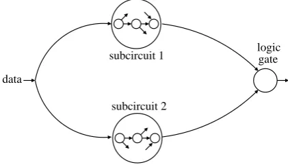
data
subcircuit 1
subcircuit 2
logic gate
Fig. 2. Signal competition within asynchronous digital circuit.
for each building block, but should be done globally about the whole circuit. The latter results in lack of techniques and CAD tools supporting the asynchronous logic-level design, as will be discussed in Sect. 2 of the paper. Here, we present our novel concept for logic-level synthesis and optimization of complex asynchronous digital circuits. It is based on the Rapid Single-Flux Quantum (RSFQ) technique for digital signal processing (Likharev and Semenov, 1991), but most of its principles can be generalized about any kind of digital electronics.
2 Timing considerations within the asynchronous digi-tal circuits
In general, the asynchronous digital circuits can be design to be Delay-Insensitive (DI) (Brzozowski and Seger, 1995), i.e. to operate properly for any delays of their components. For this, a handshaking feedback should be provided between each pair of communicating blocks, as shown in Fig. 1. In case of large-scale circuits, this leads to extremely compli-cated topologies and significant lost of speed.
Much simpler and faster circuits can be realized, if the handshaking feedbacks are omitted always when possible (Mladenov et al., 2006). Being no more DI, such an asyn-chronous circuit operates correctly under certain timing as-sumptions, whose violation leads to signal competitions, hazards, and erroneous behaviour. In order to avoid the latter, the designer should be able to detect all pairs of competitive signal paths within the circuit topology.
A signal competition occurs, if there are different paths, through which a given signal can reach one and the same component of the circuit. This is shown in Fig. 2. We have elaborated a universal approach for detection of all such
competitive structures. This approach maps the circuit un-der analysis into equivalent directed graph. By this mapping, each gate is represented as a graph’s vertex, and each inter-connect – as a directed edge with direction corresponding to the one of the signal propagation. In this way, the problem is transformed to find all pairs of directed paths between each pair of graph’s vertices. It is a conventional problem of the graph theory, whose solution has been presented in Mlade-nov et al. (2007) in details.
Once all pairs of competitive signal paths are detected, the designer should derive the conditions about their time de-lays, whose violation leads to signal conflicts. As next, it should be checked whether the violation of these conditions is possible, and such a possibility should be eliminated by proper handling of the delay times of the components of the competitive signal paths. For this, efficient techniques for modelling, manipulation, and optimization of the delay times of the circuit components should be available. We have de-veloped such techniques about the RSFQ electronics, whose basics will be described in Sect. 3.
3 Basics of the RSFQ digital electronics
The RSFQ technique has been invented in the middle of the 1980s by a team of Russian scientists (Likharev et al., 1985), who have suggested an entirely new approach for digital in-formation coding. Its switching element is the overdamped tunnel Josephson junction, consisting of two superconduc-torsS1andS2separated by a thin nonsuperconductive
bar-rier, as shown in Fig. 3.
Letθ1andθ2be the phases of the complex pair wave
func-tions of the both superconductors, andφ=θ1–θ2be their
dif-ference. LetIs be the lossless supercurrent flowing through the Josephson junction,Ic– its maximum value (also called critical current of the junction), andU (t )– the voltage drop over the junction. The electrical properties of the Josephson junction are described with:
Is =Icsinϕ(t ) (1) and
dϕ(t ) dt =
2π U (t ) 80
, (2)
with80=2.07 mV·ps being a fundamental physical constant
named the magnetic flux quantum. These relations are popular as the dc (Eq. (1)) and the ac (Eq. (2)) Josephson effect (Josephson, 1962). The balance of the currents over the junction is:
i(t ) =Is +
U (t ) R +CJ
dU (t )
withi(t )being the total current through the junction,CJ – the capacitance of the junction, andR– its normal resistance. Using Eqs. (1) and (2), Eq. (3) can be rewritten as:
i(t ) =Icsinϕ(t )+ 1
R 80
2π dϕ(t )
dt +CJ 80
2π d2ϕ(t )
dt2 . (4)
As seen from Eq. (4), the Josephson junction has equal equi-librium states, if the corresponding values of the supercon-ductive phase drop φ differ with 2π. A transient process during which φ changes with 2π is called a switching of the junction. A voltage pulse with picosecond duration is generated during such a switching, and its properties can be derived by integrating Eq. (2):
∞ Z
0
U (t ) dt =80, (5)
i.e. such a pulse carries exactly one magnetic flux quantum
80. Due to the quantizing condition expressed by Eq. (5),
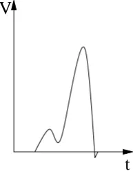
these pulses are named Single Flux Quantum (SFQ) pulses and they are used to code the binary data within the RSFQ electronics (i.e. the RSFQ electronics is pulse-based, con-trary to the classical semiconductors, where the binary data are represented by voltage levels). The typical shape of an SFQ pulse is shown in Fig. 4.
Currently, all superconductive digital circuits are based on the RSFQ technique. Within the modern roadmaps for electronics (Semiconductor Industry Association, 2005), this technique is considered as a promising alternative to the semiconductor logic not only for development of supercom-puters, but also for many advanced applications like space technologies, telecommunications, medical science, quan-tum computing, etc. Its unique features are (Likharev and Semenov, 1991):
– extreme low power consumption – the energy dissipated during one switching of single Josephson junction is of order of 10−19Joule, while the signals are commu-nicated via superconductive (i.e. lossless) transmission lines. Thus, the problem with the large power dissi-pation of the high-integrated semiconductor digital cir-cuits is not presented;
– extreme high operation speed achieved with relatively large lateral dimensions – only few years after the in-vention of the RSFQ technique, digital RSFQ circuits with micrometer features sizes operating at subTHz fre-quencies have been demonstrated (see e.g. Kaplunenko et al. (1989); Chen et al. (1999));
– intrinsically digital data representation – due to the na-ture of the flux quantization (see Eq. (5)), the different binary states are inherently defined.
Nevertheless, the RSFQ electronics still suffers from the lack of a successful large-scale application. Only few
S1
S2
U(t)
I
θ1
θ2
nonsuperconductive connection
Fig. 3. Externally shunted tunnel Josephson junction.
t
V
Fig. 4. Typical shape of an SFQ pulse.
middle-scale RSFQ devices have been reported up to now operating at clock frequencies of only few tens GHz (Bunyk et al., 2003; Tanaka et al., 2007). The big gap between the speed performance of the simple and the middle-scale RSFQ digital devices is tightly connected to the compli-cated global clock distribution network of the complex syn-chronous RSFQ digital circuits. A significant part of the to-tal circuitry of any synchronous RSFQ middle-scale applica-tion belongs to the clock distribuapplica-tion network, which leads to three negative consequences:
– a great amount of the total dc bias current is consumed by the clocking, leading to parasitic magnetic fields, which disturb the operation of the computational RSFQ electronics. Additionally, the transport of the huge dc bias current imposes severe requirements to the inter-face between the superconductive RSFQ chip and the normal conductive supply network. Both effects restrict the integration level of the RSFQ digital devices; – the global clock distribution network complicates
sig-nificantly the RSFQ layouts, often requiring “critical” structures (like crossings, vias, etc.), which may lead to parasitic interactions and provoke fabrication faults, thus diminishing the fabrication yield;
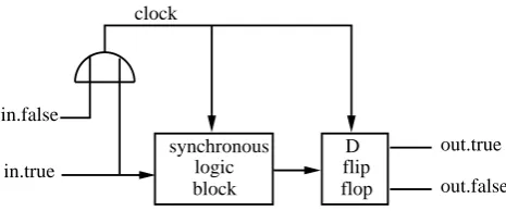
synchronous
block logic
D
flop flip clock
out.true
out.false in.true
in.false
Fig. 5. Inclusion of a synchronous logic block within an
asyn-chronous architecture based on the DR data coding: in.true and
in.false – “true” and “false” lines of the DR input channel,
respec-tively; out.true and out.false – “true” and “false” lines of the DR output channel, respectively.
restricts the minimization of the global clock interval, i.e. the high-speed performance of the large-scale syn-chronous RSFQ circuit.
All these negative effects can be more or less over-come by quantitative improvements of the currently existing RSFQ fabrication technologies and by application of new ap-proaches for design of high-integrated RSFQ digital circuits (Kang and Kaplan, 2003; Johnson et al., 2003). Neverthe-less, the design of large synchronous RSFQ circuits meets the speed of light as a fundamental physical limitation about the global synchronization. Generally, the problem with the in-creasing the global clock frequency is equivalent to reducing the geometrical size of the synchronous circuit (Sylvester and Keutzer, 2001), i.e. the product of the feature sizes and the clock frequency can be regarded as a quantitative estimation of the global synchronization problems within the densely packaged digital circuits realized with a given fabrication technology. About the modern semiconductor CPUs (fea-ture sizes below 100 nm; clock frequency of several GHz), the global clock synchronization already imposes very hard restrictions towards the further increasing of the speed and the circuit complexity (see e.g. Sylvester and Keutzer, 2001). The modern LTS RSFQ fabrication technologies have feature sizes of fewµm and intend clock frequencies of the large-scale applications above 100 GHz, i.e. their product “fea-ture sizes”דclock frequency” is of order of 1000 greater than the one of the modern semiconductor CPUs. There-fore, the realization of a synchronous RSFQ digital circuit having multigigahertz clock frequency and even approach-ing the complexity of the nowadays semiconductor electron-ics is unimaginable with the present LTS RSFQ fabrication technologies (Dimov, 2005), and the implementation of the asynchronous logic approach is a vital precondition for the overcoming of this restriction.
As already stated in this Section, the RSFQ digital elec-tronics is pulse-based, and in such a case the most reli-able asynchronous communication is provided by the Dual-Rail (DR) data coding shown schematically in Fig. 1. It
uses two lines per bit of information that has to be com-municated, which are usually named as “true” and “false” one. A pulse only in the “true” line is used for coding of Boolean “1”; a pulse only in the “false” line is used for coding of Boolean “0”, while a simultaneous propagation of pulses in both lines is forbidden. If an additional line is provided for the acknowledge signal, this communication is delay-insensitive. An important advantage of this data cod-ing is that synchronous blocks can be easily included into the asynchronous architecture (the so-called globally asyn-chronous locally synasyn-chronous circuits, see Brzozowski and Seger, 1995). The latter is shown in Fig. 5.
Based on the DR data coding, we have developed and tested an entire cell library (Dimov, 2005), containing all gates necessary for the high-level synthesis of complex asyn-chronous RSFQ digital circuits. A complete description of the schematics, the operation principles, and the electrical and time-domain parameters of its components can be found in Dimov (2004). As already stated, for the successful imple-mentation of these gates within complex asynchronous dig-ital circuits, efficient techniques for the modelling, manipu-lation, and optimization of their delay times are needed. We have developed such techniques and they are presented in the following Sections of the paper.
4 Time-domain jitter of the RSFQ electronics
4.1 Sources of time-domain jitter
Once the digital gate is designed, its nominal delay timedn can be predicted exactly e.g. by simulations. Although this constant is a very important time-domain parameter of the gate, it is quite insufficient for the logic-level design of high-speed complex circuits. The reason for this is the delay time jitter, the sources for which can be classified as:
– spread of the fabrication process: during the production of the circuit, the parameters of the fabrication tech-nology deviate stochastically from their nominal values, which leads to spread of the electrical characteristics of the fabricated circuit. The latter results in deviation of its delay time from the nominal valuedn. This is an in-evitable stochastic process, i.e. the resulting delay time cannot be determined in advance, and can be predicted only by means of the statistics;
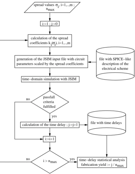
time−domain simulation with JSIM
passfall criteria fulfilled
i:=i+1
file with SPICE−like description of the electrical scheme
file with time delays
yes no
no
yes spread valuesσi
generation of the JSIM input file with circuit parameters scaled by the spread coefficients
, i=1,..,m ; nmax
i:=1 ; j:=0
calculation of the spread coefficients ki(σi), i=1,..,m
calculation of the time delay ; j:=j+1
i > nmax time−delay statistical analysis fabrication yield := j / nmax
Fig. 6. Block diagram of JSIMA:m– number of randomly gener-ated scaling coefficients,nmax– maximum number of iterations.
proportional shifting of all circuit parameters of one and the same type (e.g. all resistors, all inductances, all critical cur-rents, etc.), and the local one, which represents the random shifting among circuit parameters of one and the same type. In case of established RSFQ fabrication processes, the tech-nological parameter spread within the chip is usually negli-gibly small. Moreover, the gradients of the parameters of the operation environment are also negligibly small through the tiny circuit area. Therefore, the global spread of the delay times dominates over the local one, and for simplification of our modelling procedure, we neglect the latter.
4.2 Modelling of the delay time spread
In order to model the delay time spread of the RSFQ gates, we make the assumption, that there is no correlation between the factors determining it. As stated in Ortlepp (2005) and Dimov (2005), this assumption is not absolutely correct, but gives a good approximation due to the big number of such factors.
In this paper, we will consider only the delay time spread due to the variations of the fabrication process; however the same approach can be applied also about the spread caused by fluctuations of the operation environment. Under the assumptions done above, each global electrical parameter
+Ub
+Ub +Ub
+Ub +Ub
+Ub
+Ub +Ub +Ub
IN IN OUT1 OUT1 OUT2 OUT2 J1 J2 J3 J4 J5 J6 J7 J8 J9 J10 J12 J16 J17 J18 J19 J20 J21 J24 J25 J22 J23 L1 L2 L3 L4 L5 L6 L7 L8 L9 L10 L11 L14 L16 L17 L18 L19 L20 L21 L22 L23 L24 L25 L26 L27 L28 L29 R1 R2 R3 R4 R5 R6 J13 L15 L12 L13 R8 R9 J14 J15 R7 R10 J11
Fig. 7. Electrical scheme of the asynchronous dual-rail RSFQ 1×2 demultiplexer.
of the circuit is subjected to a Gaussian distribution hav-ing mean valueµ equal to its nominal value, and standard deviation σ being parameter of the fabrication technology. For the modelling of the impact of the fabrication spread on the delay time of the circuit, we have developed the Win-dows/DOS compatible software package JSIMSA (Mlade-nov, 2006) based on the free Josephson junction circuit sim-ulator JSIM (Fang and van Duzer, 1989). Its block diagram is shown in Fig. 6. Within one iteration loop of the program, a set of coefficients is initially generated having standard de-viations specified by the fabrication foundry. They are used to scale the nominal electrical parameters of the circuit, thus modelling their spread during the fabrication process. The resulting netlist of the circuit is simulated with JSIM, and the obtained time-domain behaviour is estimated as working (good) or not operating (bad). In case of a working circuit, it is counted and its delay time is automatically calculated and stored in a file. This cycle is repeated many (typically over 100 000) times. Finally, we build the delays’ histogram, which is analyzed by means of the statistics, thus deriving the mathematical model of the delay time distribution of the in-vestigated circuit. Additionally, we calculate the circuit fab-rication yield asj/nmax, withj – the number of the working
circuits, andnmax– the total number of simulated circuits.
We have applied this technique for statistical description about all gates from our asynchronous RSFQ cell library (see Dimov, 2004). Below, we will discuss the results about the most complex gate of the library – the dual-rail 1×2 demul-tiplexer. Its electrical scheme is shown in Fig. 7, while its element values and operation principle can be found in Di-mov (2004) and DiDi-mov et al. (2005a).
We have assumed only three independent global circuit parameters, i.e. at each iteration loop of JSIMA, we gen-erate three independent scaling coefficients – kL, ki, and
kg, subjected to Gaussian distributions with mean values
(a)
60 70 80
0 50 100 150 200 250
60 70 80
0 50 100 150 200 250
delay, ps
repetition rate
(b)
50 60 70 80 90 100
0 20 40 60 80 100 120
50 60 70 80 90 100
0 20 40 60 80 100 120
repetition rate
delay, ps
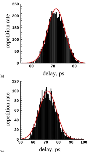
Fig. 8. Delay time spread of the 1×2 dual-rail demultiplexer in Fig. 7 caused by the technological spread: (a)σkL=σki=σkg=10%, obtained standard deviation=5.06%; (b)σkL=σki=σkg=20%, ob-tained standard deviation=9.41%.
respectively. Within the analysed circuit, we scale all induc-tances bykL, all junction critical currents and all dc bias cur-rents byki, and all junction parasitic inductances to ground bykg.
The resulting delay times are shown in Fig. 8 for the cases
σkL=σki=σkg=10% andσkL=σki=σkg=20%. As by all other gates from the cell library, the resulting statistical distribution of the delay time can be successfully fitted to a Gaussian one. The obtained large standard deviations clearly demonstrate the strong impact of the technological parameter spread over the jitter of the time-domain behaviour of the RSFQ circuits. Therefore, such an analysis should be incorporated within the derivation of the timing conditions ensuring no signal haz-ards between the competitive signal paths within the asyn-chronous digital circuits (see the discussions in Sect. 2). In this way, the delay time of each signal path is no more a con-stant value equal to the sum of the nominal delay times of the path’s components; it should be considered with its statisti-cal distribution resulting from the overlapping of the statis-tical distributions of the delay times of these components.
150 160 170 1800.050
0.055 0.060 0.065
σd
/d
σd/d
design value
spread reduction
150 160 170 180
Ic , µA
0.6 0.7 0.8 0.9 1.0
fabrication yield yield
yield degradation
optimum with respect to yield
Fig. 9. Dependence of the fabrication yield and the ratioσd/dof the asynchronous dual-rail 1×2 demultiplexer in Fig. 7 on the crit-ical currentIcof the junctionsJ14−J21. Assumed technological spread:σkL=σki=σkg=10%.
Similarly, the timing conditions ensuring hazard-free data exchange are no more Boolean variables (i.e. they can be either fulfilled or not), but have statistical nature (i.e. they can be fulfilled with a certain probability). We conclude that the exact statistical prediction of the signal conflicts is a key component of the successful design of high-speed complex asynchronous RSFQ circuits, and the proposed technique is a powerful tool for its accurate performance.
4.3 Optimization of the delay time spread
A very important and time-consuming step of the small-scale RSFQ design flow is the optimization of the cell library com-ponents (see Dimov, 2005). Within the classical synchronous RSFQ design, the goal of this step is to adjust properly the circuit’s parameters in order to maximize the gate’s fabrica-tion yield. In this way, one obtains a maximum fabricafabrica-tion yield also of the complex synchronous RSFQ digital circuit composed from these optimized gates.
As already emphasized in the beginning of this paper, the correct operation of the complex asynchronous circuits de-pends not only on the correct operation of their building blocks alone, but also on the timing assumptions allowing the omitting of handshaking feedbacks. Therefore, we opti-mize the components of our asynchronous RSFQ cell library with respect to minimize the standard deviation of their de-lay time spreads, keeping the fabrication yields reasonably large. By this, we minimize the probability of signal haz-ards within the complex asynchronous designs based on this library, keeping their yield acceptable.
delay time, a.u.
probability, a.u.
first signal path second signal path
probability of signal hazard
d1n d2n
delay time, a.u.
probability, a.u.
first signal path second signal path probability of signal hazard
d1n d2n
delay time, a.u.
probability, a.u.
first signal path second signal path
d1n d2n
Fig. 10. Overlapping of the delay time distribution of competitive signal paths: (a) without optimization of the delay times (highest
prob-ability of signal conflicts); (b) after minimization of the delay times standard deviations (reduced probprob-ability of signal conflicts); (c) after minimization of the delay times standard deviations and proper tuning of the nominal delay times (no probability of signal conflicts).
Below, we designate their value withIc, whiledandσd des-ignate the nominal value of the gate’s delay time and its stan-dard deviation, respectively. The dependence of the gate’s fabrication yield and the ratioσd/d onIcis shown in Fig. 9. The maximum fabrication yield is obtained at Ic=162µA, which is far away from the optimum ofσd/d. Therefore, we choose a nominal valueIc=175µA, reducing the fabrication yield with only few percents, but shrinking with about 10% the ratioσd/d. In this way, the time-domain stability of the gate is improved, while its yield is slightly diminished.
5 Elimination of signal conflicts within complex asyn-chronous RSFQ digital circuits
With the novel technique for minimization of the delay time spread of the RSFQ gates, one can significantly reduce the standard deviation of the delay times of the competitive sig-nal paths. In this way, the probability of overlapping of their statistical distributions is also diminished, which corresponds to reduced probability of erroneous digital operation due to signal hazards. Nevertheless, the latter can still remain un-acceptably large for high-speed complex applications. The only way for its further minimization is to manipulate the mean values of the delay times of the competitive signal paths, i.e. to tune properly the nominal delay times of their components. This is schematically shown in Fig. 10.
In Dimov and Uhlmann (2004), we have derived the pos-sible methods for manipulation of the switching speed of the Josephson junctions and compared them with respect to the following criteria:
– straightforward technological realization – the tuning of the delay times should be performed without significant redesign of the layout of the RSFQ circuit;
– minimum deterioration of the gate compatibility – ap-plying such a tuning, no parasitic interactions should occur between the circuit components. Otherwise, ex-tensive reoptimization would be necessary;
– efficient delay time tuning – the applied method should be able to manipulate precisely the RSFQ delay times
0.5 1.0 1.5 2.0
rm
−500 50
100 Xb, %Xi, %
delay, ps
Xl, %
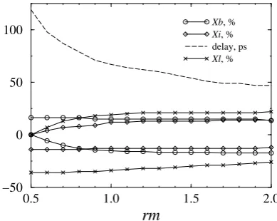
Fig. 11. Impact of the scaling of the external shunt resistors of the
Josephson junctions on the delay time and the operation margins of the asynchronous dual-rail 1×2 demultiplexer in Fig. 7: rm – scal-ing coefficient of the junctions’ external shunts; Xb, Xi, and Xl – global margins of the dc bias currents, the junctions’ critical cur-rents, and the superconductive inductances, respectively.
within large interval of values around their nominal values;
– minimum degradation of the fabrication yield and the operational margins – in this way, the reliable operation of the circuit after its production is ensured.
functional
specification structure designlogic−level gatelist
asynchronous RSFQ cell library
layout design documentation
logic−level functional
verification optimization
and speed topological
modelling RSFQ delay
passfall criteria
RSFQ delay tuning
Fig. 12. Advanced high-level design flow for complex asynchronous RSFQ digital circuits.
6 Conclusions
The signal conflicts are one of the hardest constraints for the realization of complex asynchronous digital circuits. This problem is even more pronounced within the RSFQ digital technique due to the extremely high operation speed of the Josephson junctions. In this paper, we have presented our novel techniques for detection of competitive signal paths, estimation of the probability of signal conflicts in them and its minimization by optimization of the spread of the RSFQ delay times and proper tuning of their mean values. Using these techniques, we have extended the standard logic-level design flow to an advanced design flow for complex asyn-chronous RSFQ digital circuits, which is shown in Fig. 12. In this way, the synthesis of high-performance asynchronous RSFQ digital circuits has been improved significantly.
Acknowledgements. This work is supported by the DFG research
project Uh53/4-3 and by the DAAD PPP-program (contracts DAAD-13/2005 and D/04/08637) between Ilmenau University of Technology, Germany, and Technical University of Sofia, Bulgaria.
References
Brzozowski, J. A. and Seger C.-J. H.: Asynchronous Circuits, Springer-Verlag, 1995.
Bunyk, P., Leung M., Spargo, J., and Dorojevets, M.: FLUX-1 RSFQ Microprocessor: Physical Design and Test Results, IEEE T. Appl. Supercon., 13, 433–436, 2003.
Chen, W., Rylyakov, A. V., Patel, V., Lukens, J. E., and Likharev, K. K.: Rapid Single Flux Quantum T-Flip Flop Operating up to 770 GHz, IEEE T. Appl. Supercon., 9, 3212–3215, 1999. Dimov, B.: The Asynchronous Rapid Single-Flux Quantum
(RSFQ) Logic – a Promising Alternative to the Conventional Synchronous RSFQ Electronics, http://www4.tu-ilmenau.de/EI/ ATE/kryo/asyn/index.htm, 2004.
Dimov, B. and Uhlmann, F. H.: High-Speed Asynchronous RSFQ Logic Cells with Flexible Gate Delays, IOP Publishing, Conf. Series No. 181, 3429–3436, 2004.
Dimov, B.: General Restrictions and Their Possible Solutions for the Development of Ultra High-Speed Integrated RSFQ Digital Circuits: PhD thesis at Faculty of Electrical Engineering at Il-menau University of Technology. Wissenschaftsverlag IlIl-menau, Germany, 2005.
Dimov, B., Khabipov, M., Balashov, D., Brandt, C. M., Buchholz, F.-Im., Niemeyer, J., and Uhlmann, F. H.: Asynchronous RSFQ Demultiplexer Based on Dual-Rail Information Coding, Super-cond. Sci. Tech., 18, 664–667, 2005a.
Dimov, B., Khabipov, M., Balashov, D., Brandt, C. M., Buchholz F.-Im., Niemeyer, J., and Uhlmann, F. H.: Tuning of the RSFQ Gate Speed by Different Stewart-McCumber Parameters of the Josephson Junctions, IEEE T. Appl. Supercon., 15, 284–287, 2005b.
Fang, E. S. and van Duzer, T.: A Josephson Integrated Circuit Sim-ulator (JSIM) for Superconductive Electronic Application, Ext. Abstr. 2nd ISEC, Tokyo, Japan, 407–410, 1989.
Johnson, M. W., Herr, Q. P., Durand, D. J., and Abelson, L. A.: Dif-ferential SFQ Transmission Using Either Inductive or Capacitive Coupling, IEEE T. Appl. Supercon., 13, 507–510, 2003. Josephson, B. D.: Possible New Effects in Superconductive
Tun-neling, Phys. Lett., 1, 251–253, 1962.
Kang, J. H. and Kaplan, S. B.: Current Recycling and SFQ Signal Transfer in Large Scale RSFQ Circuits, IEEE T. Appl. Supercon., 13, 547–550, 2003.
Kaplunenko, V. K., Khabipov, M. I., Koshelets, V. P., Likharev, K. K., Mukhanov, O. A., Semenov, V. K., Serpuchenko, I. L., and Vystavkin, A. N.: Experimental Study of the RSFQ Logic Ele-ments, IEEE T. Magn., 25, 861–864, 1989.
Kish, L. B.: End of Moore’s Law: Thermal (Noise) Death of Inte-gration in Micro and Nano Electronics, Phys. Lett. A, 305, 144– 149, 2002.
Likharev, K. K., Mukhanov, O. A., and Semenov, V. K.: Resistive Single Flux Quantum Logic for the Josephson-Junction Technol-ogy, SQUID’85, 1103–1108, 1985.
Mladenov, V., Todorov, V., Dimov, B., Ortlepp, Th., and Uhlmann, F. H.: Statistical Description and Optimization of the Time-Domain Parameters of Asynchronous RSFQ Digital Circuits, Proc. 51st IWK, TU Ilmenau, 145–146, 2006.
Mladenov, V., Filipova, K., Petrakieva, S., Dimov, B., and Uhlmann, F. H.: Analysis of Signal Competition in Asyn-chronous Ultra High-Speed Digital Circuits, Przeglad Elek-trotechniczny, 11, 197–200, 2007.
Moore, G. E.: Cramming More Components onto Integrated Cir-cuits, Electronics, 38, 114–117, 1965.
Ortlepp, Th.: Dynamische Analyse stochastischer Einfluesse in der supraleitenden Einzelflussquantenelektronik: PhD thesis at Fac-ulty of Electrical Engineering at Ilmenau University of Technol-ogy, Wissenschaftsverlag Ilmenau, Germany, 2005.
Semiconductor Industry Association: International Technology Roadmap for Semiconductors, http://www.itrs.net, 2005. Sylvester, D. and Keutzer, K.: Impact of Small Process Geometries
on Microarchitectures in Systems on a Chip, P. IEEE, 89, 467– 489, 2001.