,PSOHPHQWLQJD8QLTXH&KLS,'RQD5HFRQILJXUDEOH3RO\PRUSKLF&LUFXLW
/XNDV6HNDQLQD5LFKDUG5X]LFND=GHQHN9DVLFHN9DFODY6LPHN3HWU+DQDFHN
Brno University of Technology, Faculty of Information Technology, IT4Innovations Centre of Excellence
Bozetechova 2, 612 66 Brno, Czech Republic e-mail: [email protected]
http://dx.doi.org/10.5755/j01.itc.42.1.925
$EVWUDFWThe need for secure physical implementations of cryptography functions has become urgent in the recent years. In particular, a unique unclonable chip ID has been implemented using various techniques. In this paper, we investigate the use of polymorphic gates as a new mechanism for implementing a unique chip ID in systems already containing some polymorphic gates. The proposed solution exploits the fact that switching time of polymorphic gates (controlled by ܸௗௗ) is slightly different even for neighboring gates on the same die because of fabrication variations.
We applied a partial reconfiguration in order to generate 48-bit IDs on the reconfigurable polymorphic REPOMO32 chip that we have developed in our previous research. In some application scenarios, we achieved 94.44% stable bits which is reasonably close to existing approaches.
.H\ZRUGVUnclonable ID; Polymorphic Gate; Process Variation; Reconfigurable Circuit; Security.
,QWURGXFWLRQ
The requirement for security has become as much important as the functionality, cost or maintainability even for ordinary applications and systems. In this context, the security means protecting data and HW/SW systems from unauthorized access, use, modification or destruction. Classical cryptography which is based on computationally hard to break algorithms provides various solutions against some of these problems. Physical attacks such as side-channel attacks on cryptographic devices have shown that even computationally hard to break functions are not sufficient in protecting secure information when their physical implementation does not take into account the security issue. Hence we can observe an increased importance of physical security and mechanisms ensuring physical unclonable functions and data [26].
Nowadays, it is often required for some embedded systems to provide a unique unclonable identification number (ID). Typical applications where the ID could be utilized include integrated circuit (IC) identification and authentication, encryption of communication channels and intellectual property (IP) protection in case of field programmable gate arrays (FPGAs).
On-chip IDs are usually implemented either by writing a unique number to a non-volatile memory or post-fabrication modification of a chip or introducing circuits which derive unique information from inherent fabrication process variations. The last
approach has attracted a considerable attention in the recent years mainly because it represents a reasonably secure and cheap solution (see Sect. 2).
In our previous work we have developed and fabricated a small reconfigurable polymorphic chip called REPOMO32 (REconfigurable POlymorphic MOdule) [17]. The REPOMO32 chip can be programmed similarly to other digital programmable chips, by means of a configuration bit stream which defines the functionality of REPOMO32’s elementary reconfigurable blocks. In addition, however, REPOMO32 contains polymorphic gates – new electronic components whose logic function can be switched unconventionally as response to various means including power supply voltage (in our case). The main feature which distinguishes polymorphic logic from ordinary programmable logic is that a polymorphic gate does not contain any switch or multiplexer to select one of kdifferent functions. The multifunctionality is inherently embedded in the structure of each polymorphic gate. This concept has been introduced by Stoica et al. [22] and later explored by others, e.g. [6, 18].
REPOMO32 is not defined by a configuration bit stream solely. It also depends on the level of power supply voltage.
If an electronic system contains a reconfigurable polymorphic device (such as REPOMO32) it may be programmed to perform various functions that combine standard logic functionality with capabilities of sensing in one compact structure. Such systems usually contain electronic circuits enabling controlled changes of Vdd that are required in particular applications. Various applications have been proposed utilizing this concept. For a survey, see Section 3.
In this article, we present a new application of polymorphic electronics. We investigate the use of polymorphic gates as a new mechanism for implementing an unclonable ID in systems already containing some polymorphic gates. The proposed solution exploits the principle that the switching time of polymorphic gates (controlled by Vdd) is slightly different even for neighboring gates on the same die because of fabrication variations. We propose a simple circuit which compares the output signals of a pair of polymorphic gates and determines which of them has switched its logic function earlier as a response to the
Vddchange. A single bit of ID is then generated. More bits can be generated using additional polymorphic gates and comparators.
Therefore, in addition to their original function, various polymorphic systems could be equipped with a new functionality (i.e. unclonable ID) almost for free. The experimental evaluation of the proposed method has been carried out using 21 (universal) REPOMO32 chips, i.e. we have not designed a new chip to perform the experiments. The results show that the proposed scheme is able to produce unique and reasonably non-colliding IDs.
The rest of the paper is organized as follows. Section 2 briefly introduces the area of on-chip IDs. The REPOMO32 chip, which will be used for experimental evaluation, is described in Section 3. Section 4 deals with the proposed implementation of on-chip ID using the REPOMO32 chip. The results, which include the ID collision analysis and ID stability analysis, are summarized in Section 5. Conclusions are given in Section 6.
8QLTXH2Q&KLS,'
Obtaining a unique ID from a chip is a problem very similar to the unique cryptographic key generation problem. We need a number which is unique to a particular chip and does not change during time. The first implementations of the on-chip IDs were based on writing a unique number to a non-volatile memory or post-fabrication modification of the chip using lasers or fuses. In 2000, Lofstrom et al. proposed a new method utilizing inherent process variations that exist from die to die for obtaining a unique ID [8]. Unlike post-fabrication creating of IDs,
the ID codes are assigned randomly here. Recently published papers have shown that a unique ID can be extracted from each chip by comparing variations in transistors characteristics [23], digital path delays [10, 24] or random initialization states of static RAM cells [4], i.e. by utilizing the features that are undesirable in common digital circuits [2]. However, traditional delay-based solutions exploit only IC's process variations for ID generation.
More advanced approaches have utilized equivalent resistance variations in the power distribution system [5] and variations of environment (temperature, power supply noise and crosstalk) [27]. A detailed survey and classification can be found in [12].
As physical variations creating the ID are below the resolution of the manufacturing equipment it is difficult for an attacker to make a reasonably good clone of the chip. Unfortunately, the output values can not directly be used as a unique ID because approximately 4-5% bits are unstable [28]. Hence any implementation must ensure that each particular chip is identified with a very high probability. In particular, determining a sufficient number of bits for each ID and ensuring high stability in an operational environment (noise, unstable Vdd) are crucial for obtaining highly stable ID codes. An analysis of the probability of misidentification has been performed for different unstable bit percentages in [23].
,'&ROOLVLRQV
There is a finite probability of the ID code collision within a given number of chips. Following the analysis given in [23], ID collision between any two chips can be expressed as 1/2X where X is the
number of bits in an ID code. The total probability of ID collision across Ychips can be expressed as
Yn X
c
n
P
1
)
2
1
1
(
1
(1)Figure 1 shows the ID collision probability versus different number of chips Yfor various ID lengths. It can be seen that the use of randomly assigned IDs might be highly reliable for many applications. The collision probability is less than 10-9 even for short
IDs (64 bits) when 10 thousand chips are fabricated.
5HTXLUHPHQWVRQ,'V
)LJXUHProbability of ID collision versus different number of chips for various ID lengths
)LJXUHThe REPOMO32 chip shown together with the implementation details of a single CLE block and NAND/NOR gate
The Hamming distance between the ID codes obtained from two different chips should be, on average, half of the total number of bits in the ID. The average Hamming distance significantly below X/2 indicates that there are many collisions and the underlying variations of physical process are not sufficient. In order to make a potential attack even more difficult the number of zeros has to be as close as possible to the number of ones in every ID.
Performing of the analysis of the average Hamming distance, determining of the number of unstable bits and measuring of the zero-one
distribution is important for evaluation of any proposal in this area.
5HFRQILJXUDEOH3RO\PRUSKLF&KLS
is presented in this paper, employs polymorphic gates originally proposed in 2008 [15].
The main motivation for development of polymorphic electronics is potentially very fast and cheap reconfiguration of polymorphic gates, e.g. by means of Vdd. Current applications of polymorphic electronics include multifunctional circuits (counters [13] and filters [16]), test vector reduction [18] and self-testing circuits [11, 29]. Since conventional tools do not support synthesis of polymorphic circuits, various design and optimization methods have been proposed in this domain [3, 9, 19]. They typically combine classic approaches (such as Binary Decision Diagrams or satisfiability problem solving) with evolutionary computing. Theoretical research in this area has lead to a new completeness theory for polymorphic Boolean networks [7].
A recent work that falls into this context has shown a novel graphene reconfigurable logic device based on the control of p-n doping configurations using split gates [25]. By using split gates to change the grapheme properties, multi-function logic gate was obtained and dynamically reconfigured. This kind of devices is considered as a new way for implementing some reconfigurable electronic systems. We can speculate that, for example, Tabula’s 3D Spacetime FPGAs [1] could benefit from it in the future.
In order to demonstrate crucial features of elementary polymorphic circuits (such as small polymorphic combinational circuits), the REPOMO32 chip has been developed and tested [17].
5(3202
REPOMO32 is primarily intended for implementation of polymorphic four-input/four-output combinational circuits. As Fig. 2 shows, the chip consists of 32 two-input Configurable Logic Elements (CLEs) organized in an array of 4 rows and 8 columns. A CLE can be programmed to perform one of the following functions: AND, OR, XOR and polymorphic NAND/NOR (controlled by Vdd). When
Vdd = 3.0 - 3.8 V the NAND/NOR gate exhibits the NOR function and when Vdd = 3.9 - 5V the gate exhibits the NAND function. Remaining gates do not change their logic functions with changes of Vdd
within the range of 3 - 5 V.
REPOMO32's logic behavior is defined by its configuration bits and the level of Vdd. The configuration bits control a set of multiplexers which are responsible for interconnecting the CLEs and selecting their logic functions. In total, 8 bits define the configuration of a single CLE. The configuration of the chip is stored in 32 8-bit latch registers. The configuration of a single CLE is performed by supplying CLE's address (addr)and configuration data (data)followed by activating the WE signal. The chip can completely be reconfigured in 32 configuration steps. The primary outputs Z0 … Z3 are connected directly to CLEs of the last column. There are no
synchronization registers in REPOMO32. The chip has 28 pins and occupies the area of 2900 u1970Pm.
It was fabricated using AMIS CMOS 0.7 Pm
technology.
The REPOMO32 chip is considered as a small module which may be embedded into a larger system. Note that REPOMO32 is not intended for implementing an unclonable ID. However, we will show that it can be programmed to obtain a basic unclonable ID.
5(3202.LW
A REPOMO32/kit is a dedicated experimental board which has been designed with the aim to conveniently facilitate test, evaluation and measurement procedures of all the features available inside the REPOMO32 chip [20]. This evaluation platform contains a DIL-28 socket for an integrated circuit with polymorphic gates (REPOMO32 chip), which may be configured by means of external switches or signals. A set of fast buffers is deployed in order to separate available input ports from the surrounding environment. The REPOMOKit also contains a Xilinx XC9572XL CPLD which may be used as a configuration controller for REPOMO32 or to customize an additional application-specific logic.
A special attention has been paid to the power generation and distribution across the board. Flexible power system is virtually divided into several independent branches, which deliver power supply within a range of 3.3–5V to the individual components onboard. It consists of dedicated rails for on-board auxiliary logic and a set of programmable power sources for the REPOMO32 chip itself. For example, the user may choose between stabilized 3.3/5V voltage in either manual way or by means of using a signal from external controller or logic. Another feasible alternative how to obtain Vddis based on using programmable power supply, which makes it possible to generate an eligible level of the output voltage within the range of 3.3-5V. A digital potentiometer and integrated microcontroller are employed for this task. The REPOMO32/kit contains a dedicated heated chamber which is used to create special kind of working environment, where the temperature may reach up to 150 °C. The whole conception is based around metal box with dimensions of 76 mm u48 mm
subsequently managed by an 8-bit MCU, in particular MC9S08QE8 manufactured by Freescale. Its tasks include processing of test parameters, temperature measurement with sensor ADT7301 and heating regulation by means of switching power to the spiral heating wire. Temperature measurement can be carried out with a resolution of 0.03125 °C, which is more than sufficient for the character of REPOMO32 chip thermal analysis.
0HDVXUHPHQWRQ3RO\PRUSKLF*DWHV
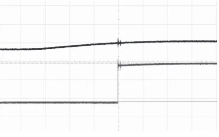
Dynamic characteristics of polymorphic gates of REPOMO32 chip were investigated for normal temperature in [20]. Fig. 3 shows the output of the NAND/NOR gate when the chip is exposed to supply voltage ramp up from 3.3 V to 5 V level. In order to observe a change on the output logic signal, the NAND/NOR gate has different logic values assigned at its input ports (i.e. the 01 or 10 combination).
Fig. 4 shows a delay of one particular critical path created using four CLEs (one of them configured as the NAND/NOR) in the REPOMO32 chip as a function of temperature. It can be seen that the length of critical path tpdis almost constant to approx. 100°C. After this limit, tpdrises significantly. It means that the chip goes slower for high temperatures. Note that the experiment was performed for Vdd = 3.3 V on four randomly selected chips. The results of experiments show that there are no significant differences among chips for traditional temperature range [14].
)LJXUH 3Response of a polymorphic NAND/NOR gate (down trace) exposed with supply voltage ramp up from the
3.3V to 5V level (upper trace). The inputs of the NAND/NOR gate are set at '0' and '1'. Time base is 1 Ps/div
)LJXUHCritical path length vs. temperature for four
selected chips
8QFORQDEOH,'RQ5(3202
Implementing of unclonable ID on the REPOMO32 chip is a challenging task since REPOMO32 has been designed for completely different purposes. The proposed solution is based on the fact that the switching time of polymorphic gates (controlled by Vdd) is slightly different even for neighboring gates on the same die because of fabrication variations. There are several constraints that have to be considered when polymorphic gates of the REPOMO32 chip are utilized for unique ID generation.
x Since there are only four outputs it is possible to produce only a few bits of a particular ID in one step.
x Since there are not direct connections from primary inputs to CLEs that are situated in columns 2-8 it is necessary to configure some CLEs as wires (i.e. identity function) to make connections from the primary inputs to particular CLEs.
x Since no data registers exist in the REPOMO32 chip the resulting ID must be stored in an external register.
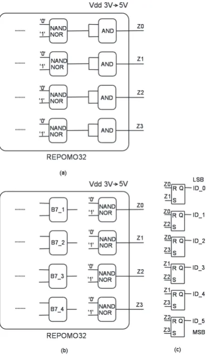
The proposed solution overcomes these problems by a partial reconfiguration of the REPOMO32 chip. The resulting ID is then generated in several steps. As only four primary outputs are available, we use only four polymorphic gates (one column of CLEs) to generate a part of the ID in one step. Fig. 5b shows that the outputs of four polymorphic gates which are configured as NAND/NORs are connected to a set of S-R (set reset) latches (Fig. 5c). The S-R latches may be implemented either on an external chip (on the CPLD in our case) or as a part of our future polymorphic reconfigurable device. An S-R latch determines which of two polymorphic gates has switched its logic function earlier as a response to the
Vdd change (3V o 5V.). The resulting bit is then considered as one bit of the ID. It is necessary to ensure that the inputs of the NAND/NOR gates are fed by mutually inverse logic values to invert the output value of the gate with the change of Vdd. These values come from the primary inputs via CLEs (situated in columns 1-7) that must be configured to operate as wires (e.g. using the AAND A=Asetting).
Therefore, the unique bits are obtained when Vddis changed and under assumption that physical characteristics (delays during switching) of pairs of gates differ from die to die.
)LJXUHThe on-chip ID on REPOMO32: (a) The NAND/NOR gates configured to column 7; (b) The NAND/NOR gates configured to column 8; (c) The S-R
circuits used to generate and store the ID
remaining columns are configured as “wires”. The S-R latches are reused. This strategy is illustrated for columns 7 and 8 in Fig. 5a, b. The initial configuration requires 32 configuration steps (all CLEs have to be configured). A 6-bit ID is extracted using the first column of CLEs (configured as the NAND/NOR function) while columns 2–8 operate as “wires”. Then, in order to obtain next 6 unique bits, 8 CLEs (located in columns 1 and 2) have to be reconfigured (the first column is now the “wire”; the second column performs the NAND/NOR functions). The same strategy is repeated for remaining columns. In total, eight 6-bit IDs can now be produced using a single REPOMO32 chip.
0HDVXUHG5HVXOWVDQG'LVFXVVLRQ
In order to evaluate the proposed method, IDs were measured for 21 REPOMO32 chips available to us. Table 1 gives the 6-bit IDs obtained for all columns of all the chips. We repeated the measurement 1000 times for each chip to establish the number of unstable bits. The resulting average number of unstable bits varies from 5.56% (column 8) to
17.94% (column 2) as shown in the last section of Table 1. We hypothesize that lower values measured for columns 5-8 are due a closer connection of polymorphic gates to the S-R circuits; i.e. delays which may introduce errors are more stable. The average number of unstable bits is 11.08 % when the whole 48-bit ID is considered.
7DEOH The 6-bit ID obtained from each column for 21 REPOMO32 chips (A-U)
7DEOHMeasured Hamming distance of the ID codes for all combinations of 21chips (A-U)
Table 2 shows the Hamming distances obtained for 48-bit IDs. The average Hamming distance is 22.83r4.11 (see the histogram in Fig. 6) which is a value reasonably close to the theoretical value 24.
Figure 7 shows the average Hamming distance for IDs containing 6, 7…24 bits that were obtained from columns 1-4 and 5-8. It can be seen that more reliable IDs were obtained using columns 5-8. In order to obtain collision free IDs, 10 bits are sufficient for our set of 21 chips. The ratio of the number of “1” vs the number of “0” is 1.25 in the 48-bit IDs.
)LJXUHHistogram of Hamming distances for 48-bit IDs
)LJXUHThe average Hamming distance of ID codes vs the
number of bits in IDs for columns 1-4 and 5-8
total. We observed different quality of IDs read from different columns of the chip. The quality of generated IDs may be increased by introducing various error correction codes as proposed e.g. in [28].
A straightforward approach to implementing a k -bit signature in a future polymorphic ASIC is the utilization of a sufficient number of independent polymorphic gates and their direct connection with the S-R latches.
In comparison with the implementation proposed in this article, that approach would lead to a much faster ID generation (no reconfiguration will be needed) and increasing the quality of IDs as the number of unstable bits would be around 5.56% (see column 8 in Table 1).
&RQFOXVLRQVDQG)XWXUH:RUN
In this paper, we showed that polymorphic electronics can be utilized to implement unique on-chip IDs. We applied a partial reconfiguration in order to generate 48-bit IDs on the REPOMO32 chip. If IDs were obtained from polymorphic gates connected directly to the S-R circuits (i.e. from column 8 of REPOMO32) only 5.56% bits are unstable which is a result reasonably close to existing approaches achieving 4% on ASIC [23] and FPGA [4].
Future work will consists of replacing our reconfigurable chip by a new chip specialized for this application where a sufficient number of polymorphic gates will be directly connected to the S-R latches. We will also introduce a suitable error correcting scheme.
$FNQRZOHGJHPHQWV
This work was partially supported by the Czech Science Foundation under project Natural Computing on Unconventional Platforms P103/10/1517, the research program Security-Oriented Research in Information Technology MSM 0021630528, the BUT project FIT-S-11-1 and the IT4Innovations Centre of ExcellenceCZ.1.05/1.1.00/02.0070.
5HIHUHQFHV
[1] Abax Product Family Overview. URL: www.tabula.com, 2012
[2] (%DUHLãD9-XVDV.0RWLHMnjQDV5âHLQDXVNDV
Delay Fault Models and Metrics. In: Information Technology And Control, 2005, Vol. 34, No. 4, pp. 307-317.
[3] = *DMGD / 6HNDQLQDOn evolutionary synthesis of compact polymorphic combinational circuits. In:
Journal of Multiple-Valued Logic and Soft Computing, 2011, Vol. 17, No. 6, pp. 607-631.
[4] -*XDMDUGR66.XPDU*-6FKULMHQ37X\OV
FPGA intrinsic PUFs and their use for IP protection. In: Cryptographic Hardware and Embedded Systems Workshop, LNCS 4727, Springer, 2007, pp. 63-80. [5] 5+HOLQVNL'$FKDU\\D-3OXVTXHOOLFA physical
unclonable function defined using power distribution system equivalent resistance variations. In: Proc. of Design Automation Conference, ACM, 2009, pp. 676-681.
[6] '+HQWULFK (2UXNOX -6DQLLH Polymorphic Computing: Definition, Trends, and a New Agent-Based Architecture. In: Circuits and Systems, 2011, Vol. 2, No. 4, pp. 358-364.
[8] ./RIVWURP :5'DDVFK '7D\ORU IC identification circuit using device mismatch. In:Proc. of the IEEE International Solid State Circuits Conference, IEEE, 2000, pp. 372–373.
[9] :/XR==KDQJ;:DQJDesigning polymorphic circuits with polymorphic gates: a general design approach. In:IET Circuits, Devices & Systems, 2007, Vol. 1, No. 6, pp. 470-476.
[10]$0DLWL 15DJKXQDQGDQ $5HGG\ 36FKDXPRQWPhysical unclonable function and true random number generator: A compact and scalable implementation. In: Proceedings of the 19th Great Lakes Symposium on VLSI. ACM, 2009, pp. 425-428. [11]00DVKD\HNKL ++$UGDNDQL $2PLGLDQ A
new efficient scalable bist full adder using polymorphic gates. In: World Academy of Science, Engineering and Technology Journal, 2010, Vol. 61, pp. 283-286.
[12]85KUPDLU\ 6'HYDGDV ).RXVKDQIDUSecurity based on Physical Unclonability and Disorder. In:
Introduction to Hardware Security and Trust, M. Tehranipoor and C. Wang (ed.), Springer, 2012, pp. 65-102.
[13]55X]LFND Gracefully degrading circuit controllers based on polytronics. In: Proc. of 13th Euromicro Conference on Digital System Design.IEEE Computer Society, 2010, pp. 809-812.
[14]55X]LFND 96LPHN /6HNDQLQD Behavior of CMOS Polymorphic Circuits in High Temperature Environment. In: Proceedings of the 2011 IEEE Symposium on Design and Diagnostics of Electronic Circuits and Systems. IEEE CS, 2011, pp. 447-452. [15]55X]LFND /6HNDQLQD 53URNRS Physical
demonstration of polymorphic self-checking circuits. In: Proc. of the 14th IEEE Int. On-Line Testing Symposium.IEEE Computer Society, 2008, pp. 31-36. [16]/6HNDQLQD55X]LFND=*DMGDPolymorphic FIR filters with backup mode enabling power savings. In:
2009 NASA/ESA Conference on Adaptive Hardware and Systems, IEEE, 2009, pp. 43-50.
[17]/6HNDQLQD 55X]LFND =9DVLFHN 53URNRS /)XMFLN Repomo32 – New reconfigurable polymorphic integrated circuit for adaptive hardware. In: 2009 IEEE Workshop on Evolvable and Adaptive Hardware,IEEE CIS, 2009, pp. 39-46.
[18]/6HNDQLQD /6WDUHFHN =.RWDVHN =*DMGD
Polymorphic gates in design and test of digital circuits. In: Int. Journal of Unconventional Computing, 2008, Vol. 4, No. 2, pp. 125-142.
[19]/6HNDQLQD =9DVLFHN A SAT-based Fitness Function for Evolutionary Optimization of Polymorphic Circuits, In: Proc. of the 2012 Design,
Automation and Test in Europe, Dresden, EDAA, 2012, pp. 715-720.
[20]9 6LPHN 5 5X]LFND / 6HNDQLQDOn analysis of fabricated polymorphic circuits. In: Proc. of the 13th Int. IEEE Symposium on Design and Diagnostics of Electronic Circuits and Systems, IEEE, 2010, pp. 281-284.
[21]$6WRLFD 5=HEXOXP ;*XR '.H\PHXOHQ ,)HUJXVRQ 9 'XRQJ Taking Evolutionary Circuit Design From Experimentation to Implementation: Some Useful Techniques and a Silicon Demonstration. In: IEE Proc.-Comp. Digit. Tech., 2004, Vol. 151, No. 4, pp. 295-300.
[22]$6WRLFD 56=HEXOXP '.H\PHXOHQ
Polymorphic electronics. In: Proc. of Evolvable Systems: From Biology to Hardware Conference. LNCS 2210, 2001, pp. 291-302.
[23]<6X -+ROOHPDQ %32WLV A digital 1.6 pj/bit chip identification circuit using process variations. In:
IEEE Journal of Solid-State Circuits, 2008, Vol. 43, No. 1, pp. 69-77.
[24] *(6XK6'HYDGDV. Physical unclonable functions for device authentication and secret key generation. In:
Proc. of Design Automation Conference.ACM, 2007, pp. 9-14.
[25]67DQDFKXWLZDW -8/HH ::DQJ &<6XQJ
Reconfigurable multi-function logic based on graphene p-n junctions. In: Design Automation Conference. ACM, 2010, pp. 883-888.
[26]07HKUDQLSRRU &:DQJ (GV Introduction to Hardware Security and Trust. Springer Verlag, Berlin, 2012, pp. 195-229.
[27];:DQJ 07HKUDQLSRRU Novel physical unclonable function with process and environmental variations. In:Proc. of Design, Automation and Test in Europe, 2010, pp. 1065-1070.
[28]+<X 3+:/HRQJ ++LQNHOPDQQ /0|OOHU 0*OHVQHU 3=LSI Towards a unique fpga-based identification circuit using process variations. In:19th International Conference on Field Programmable Logic and Applications. IEEE, 2009, pp. 397-402. [29]56=HEXOXP $6WRLFD. Multifunctional Logic
Gates for Built-In Self-Testing. NASA Tech Briefs.
Vol. 30, No. 3, 2006, p. 10.
[30]'3$JUDZDO 4$=HQJ Introduction to Wireless and Mobile Systems, Thomson Brooks, 2003, ISBN 0534-40851-6.