INTERNATIONAL JOURNAL OF ENGINEERING SCIENCES &
MANAGEMENT
AUTHENTICATION WITH AES CRYPTOGRAPHIC ENCRYPTION CHIP DESIGN AND SIMULATION
Nitin Gupta*, Manoj Kumar
*Research Scholar, Mewar University,Chhittorghara, India Dept. of Mathematics,R.K. (P.G.) College Shamli,U.P.,India
ABSTRACT
Authentication is an indispensable part of Cryptography, which is an unconditionally secure key distribution technique based on the laws of nature. The paper explains the encryption technique using AES algorithm with 128 bits block size and 128 bit key size. The design is developed using S box technique with optimal hardware solution with the help of VHDL programming language. The design is synthesized on Vertex-5 FPGA using Xilinx 14.2 software and Modelsim 10.1 b. The algorithm is implemented to work in software and the file is to be encrypted in software and transferred to the machine containing the FPGA, which guarantees the secured communication and authentication. The concept of secured communication can be authenticated ATM machines, smart devices, biometrics applications and password protected devices. Remote authentication schemes allow a valid user to login a remote server and to access the services provided by the remote server over an insecure channel. Password based authentication schemes are the most widely used techniques for remote user authentication. Password based remote user authentication schemes are used to check the validity of a login request made by a remote user.
KEYWORDS: Advanced Encryption Standard (AES) method, Encryption and Decryption, Field programmable gate Array (FPGA).
INTRODUCTION
been the traditional and widely accepted tool of authentication .A valid user enters his/her password and host confirm it from the user every time he /she tries to log in[2, 5].
AES ALGORITHM
AES is based on the Rijndael cipher and developed by two Belgian cryptographers, Vincent Rijmen and Joan Daemen. They submitted a proposal to NIST during the AES selection process.Rijndael is a family of ciphers with different key and block sizes. TheAdvanced Encryption Standard(AES) [2, 4 ,11] is standardized by the U.S. National Institute of Standards and Technology (NIST) in 2001 and is a specification for the encryption of electronic data established. For AES, NIST selected three members of the Rijndael family, each with a block size of 128 bits, but three different key lengths: 128, 192 and 256 bits. U.S government has been adopted AES and is now accepted worldwide. It is the advanced version of DES algorithm developed in 1977. The algorithm used in AES is based on symmetric key approach in which same key is shared by both encrypting and decrypting. In the US, AES was announced by the NIST as U.S. FIPS PUB 197 (FIPS 197) on November 26, 2001. This announcement followed a five-year standardization process in which fifteen competing designs were presented and evaluated, before the Rijndael cipher was selected as the most suitable. After the approval of Secretary of Commerce, AES became effective as a federal government standard on May 26, 2002. AES is included in the ISO/IEC 18033-3 standard. AES is available in many different encryption packages. AES is the first publicly accessible and open cipher approved by the National Security Agency (NSA) for top secret information when used in an NSA approved cryptographic module. The criteria defined by selecting AES fall into three areas Security, Implementation and cost of the algorithm. The main emphasis was the security of the algorithm to focus on resistance of cryptanalysis attacks, implementation cost should be less so it can be used for small devices like smart cards. The AES algorithm is a private key block cipher. It encrypts data of block size 128 bits. It uses three key sizes, 128 bits, 192 bits and 256 bits in three versions. AES uses three different types of round operations. Table I shows the number of rounds in three versions of AES. But, in each version final round key is 128 bits.
Table I: Round key size and number of rounds in three versions of AES [11, 14]
Cipher Key size No. of rounds Round Key Size
128 bits 10 128 bits
192 bits 12 128 bits
256 bits 14 128 bits
Fig.1 AES encryption with shift row transformations [11, 16]
Replacement of DES, Excellent security, limited key size. . It encrypts data of block size 128 bits. It uses three key sizes, 128 bits, 192 bits and 256 bits in three versions. AES uses three different types of round operations
Fig.3 Subbyte Transformation [11]
The first transformation is Subbytes transformation used for encryption and inverse Sub Bytes used for decryption. The transformation is a nonlinear byte substitution that operates independently on each byte of the State using a substitution table (S-box). In the method multiplicative inverse is taken in the finite field GF (28) and affine transform to do the Subbytes transformation. In the inverse affine transform values have to find for inverse Subbytes transformation then multiplicative inverse of that byte. In the fig 3. it is indicated, the usage of the transformation can be done. There are two hexadecimal digits x and y in one state element, the left digit (x) defines the row and the right digit (y) defines the column of the substitution table. The junction of these two digits is the new bytes. Inverse Subbytes transformation is a method of inverse of Subbytes transformation. It is also possible to find in the similar way only table which is used for mapping the byte is different. The Subbytes transformation is done through S-box technique. There are two techniques to perform substitutions, (i) using composite field arithmetic (ii) using S-BOX table.
In the AES algorithm, there are four steps like Sub Byte, Shift Row, Mix Column and Add Round Key in normal rounds. The design consideration highlights some following modifications:
Exclusion of shift row transformation
Pipelining for high throughput with pipelined structure [17]
Design optimization to keep handy balance between throughput and Silicon area
Exclusion of Shift Row Transformation
Fig.4 (a) Row Transformation [15]
Fig.4 (c) LUT with matrix [14]
In the AES algorithm, the primary requirement is of high data rate. High data rate can be achieved with the help of pipelined architecture. Pipelining is not for whole rounds required for encryption/decryption but one main constraint is that pipelining is only possible within each round. Further round can start only when previous round is totally completed as input data of the next round solely depend on the output of the previous rounds. Therefore, the design mainly concentrates on pipelined architecture implementation and methodology of each round. The design is optimized to keep handy balance between throughput and silicon area. There are different types of hardware architectures for AES algorithms are possible. The best architecture is one which is having the best tradeoff between clock speed and silicon Area for higher throughput. S-Box [15] transformation uses least 16 cycles are required to process 16 elements through S Box, if it is assumed in each cycle one element is processed through. Each AES round is having 4 steps. Using pipelined structures within each round, total cycles required (for 10 round of AES Algorithm for 128 bit data & 128 bit key) is approx 220 cycles. Here silicon area is saved but losing high data throughput. In the extreme case, whole 10 rounds can be completed within 44 cycles using 16 SBox (LUT). In this case, though high throughputs are achieved, silicon area may be too much wasted. So our design mainly keeps the compromise between data throughput and silicon area in FPGA by introducing 4 SBox (LUT). Here whole encryption / decryption round completes within approx 90 cycles.
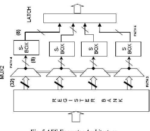
ENCRYPTOR ARCHITECTURE
Fig. 5 AES Encryptor Architecture
Encryption process starts, after the key expansion is over. First of All, in encryption process, a pre round has to be performed which XORs the original 128 bits of input data with the original 128 bits of key and the intermediate result is stored in the register bank. Once the pre round is over then the remaining rounds of operation are performed. These rounds processed in the following manner: Intermediate register bank is used to read the data applied to four 4x1 mux of 32 bits from where the selected data is feed to the input of S-box. The S box transforms the data to their corresponding transformed data and pass it to mix column stage for further processing. The Mix column stage gets these 32 bits of data and according to the algorithm multiplies the data with a standard matrix to produce a 32 bit output. Now this output is applied to the Add Round Key[16, 17] which also has the 32 bits input from the key memory. These two 32 bits inputs are XORed in this module and are getting stored in the intermediate Register Bank again for the next round. Therefore, with the help of pipeline structure, all the four column of the new intermediate matrix are obtained one after the other keeping all the modules of the design busy all the time. In the last round, Mix Column stage is skipped and the result from the Add Round Key is gets stored in the output cipher text Memory. The proper selection of the module and data path for a particular round is done by the FSM controller [3]. The Controller also controls the Key Scheduling module so that valid keys are called for the particular round. The whole procedure of encryption is done for 128 bits plain text and 128 bits key in 88 cycles excluding the 62 cycles for the key expansion module. But the key expansion overhead does not cause degrading of the performance because for a input of larger size, the same expanded keys are again and again.
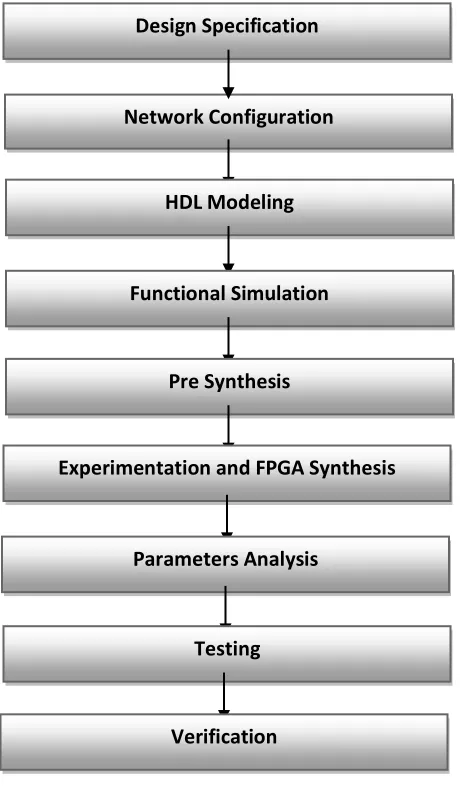
METHODOLOGY
Fig. 6 Steps in methodology
Design Specification: In design specifications the designer decides to develop the chip either in top down or bottom up approach. In bottom up approach the circuit is designed using micro module to form a design and top down approach a design is distributed in sub modules. In the multistage networks bottom up approach is utilized to implement the design.
Network Configuration: The designer has to choose the cluster size of the design. In the case of particular network, the block size and key size may be dependent or variable.
HDL Modeling: The designer has to understand the feasibility to design with the supporting languages such as
VHDL, Verilog HDL, and System C etc. The designer also decides the modeling of chip and design constructs in data flow, behavioral and structural model.
Functional Simulation: The designed modules are checked according to their functionality and test cases. The
functional simulation depends on the test benches developed by the designer, clock frequency and reset circuitry.
Pre Synthesis: Pre synthesis includes the RTL simulation, device synthesis report contains the summary of hardware parameters with combinational and sequential circuit. If the hardware utilization is greater than the 100 % for the configured device, the designer has to redesign and check for the optimized device and timing parameters.
Experimentation and FPGA Synthesis: The experimental setup is arranged to check the functionality of chip with its compatibility and interfacing to FPGA board. The maximum support frequency of FPGA board is analyzed to check the data transfer rate. In the experimental setup inputs can be through switches, and output
Network Configuration Design Specification
HDL Modeling
Functional Simulation
Pre Synthesis
Experimentation and FPGA Synthesis
Parameters Analysis
Testing
can be analyzed with the help of LEDs. There is inbuilt ADC and DAC in Virtex 5 FPGA to check the real time functionality.
Parameters Analysis: The FPGA source and target parameters are analyzed with the help of optimized FPGA
results. Static timing analysis and device utilization is also analyzed with minim speed grade and memory utilization.
Testing: The synthesized results are tested for the different test cases and combination with the help of LUTs. In the multistage network the inlets and outlets functionality is checked for maximum combination, inert and interexchange communication. The developed chip is also tested for analog input given to FPGA and processed output signals on DSO. The signal characteristics are also tested with the FPGA device compatibility and display unit.
Verification: The Design Under Test (DUT) is verified with timing parameters and test cases. Standard VHDL
has all the features necessary to code randomization of stimulus and functional coverage, both are very important while verifying larger, system-level designs. Verification is used to describe testing of a group of logic using a test bench, implemented for every verification level.
RESULTS AND DESCRIPTION
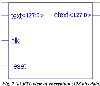
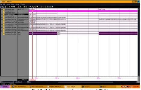
The simulation results RTL view of the chip is a top view representation depicting its pins details and input/ output logic. The possible inputs and ouputs used in the development of the chip are represented with their RTL view.
Fig. 7 (a) RTL view of encryption (128 bits data)
Fig. 5 (b) Modelsim output waveform of encryption (128 bits)
The description of the pins in listed in table 2
Table 2 Pins for AES encryption logic Pins Description
text Input text of the encryption end it can be of ‘N’ bits, simulation results show for 128 bits. It is of std_logic_vector type
clk clk is used for synchronization and provide clock pulse to work digital logic at duty cycle reset Reset is used to reset the logic circuitry and synchronized with clock pulse of rising edge
ctext Ciphex text is the text which is encrypted at the transmitting end. It can be any garbage value and it is of std_logic_vector type
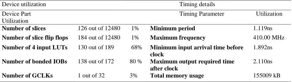
Table 3 Utilization in AES Design
Device utilization Timing details
Device Part Utilization
Timing Parameter Utilization
Number of slices 126 out of 12480 1% Minimum period 1.119ns Number of slice flip flops 184 out of 12480 1% Maximum frequency 410.00 MHz
Number of 4 input LUTs 130 out of 189 68% Minimum input arrival time before clock
1.892ns
Number of bonded IOBs 138 out of 172 80 % Maximum output required time after clock
2.110ns
Number of GCLKs 1 out of 32 3% Total memory usage 155009 kB
CONCLUSIONS
Remote users can be authenticated using passwords, smart cards etc. The authentication is integrated with Cryptographic AES encryption and decryption logic. The AES algorithm for encryption logic is implemented by selection of key and block size bits (128 bits).For higher throughput, 16 S-Box is used completing whole processes. In future work can be carried out for encryption and decryption of video. The proposed implementation is more efficient and suitable for hardware critical applications, and authenticate secured transmission with password facility. An optimized coding for the implementation of Rijndael algorithm for 128 bits has been developed which results in a throughput of Virtex 5 FPGA device. Architectural and algorithmic optimization like pipelining, exclusion of shift row, on the fly round key generation has been incorporated in the design.
REFERENCES
1. Ashwini M. Deshpande, Mangesh S. Deshpande and Devendra N. Kayatanavar, “Implementation of AES Encryption and Decryption” International Conference on “Control, Automation, Communication and Energy Conservation -2009, (page 1-5)
2. A. Hodjat and I. Verbauwhede, "Area-throughput trade-offs for fully pipelined 30 to 70 Gbits/s AES processors," IEEE Transactions on Computers, vol. 55, pp. 366-372, Apr. 2006.
3. Adesh Kumar, Sonal Singhal, Piyush Kuchhal “Network on Chip for 3D Mesh Structure with Enhanced Security Algorithm in HDL Environment” International Journal of Computer Applications (0975 – 8887) Volume 59– No.17, December 2012, pp(6-12)
4. B. Gladman, "A Specification for Rijndael, the AES Algorithm." [Online]. Available:http://fp.gladman.plus.com/cryptography_technology/rijndael/aesspec.pdf.
5. Cheng Wang and Howard M. Heys “Using a Pipelined S-Box in Compact AES Hardware Implementations” 2010 IEEE Xplorer, pp(101-105)
6. I. Hammad, K. E. Sankary and E. E. Masry, “High-Speed AES Encryptor With Efficient Merging Techniques,” IEEE Embedded Systems Letters, Vol.2 (3), pp.67- 71, Sept. 2010.
7. J. M. G. Criado, M. A. V. Rodriguez, J. M. S. Perez, J. A. G. Pulido, “A new methodology to implement the AES algorithm using partial and dynamic reconfiguration,” Integration, the VLSI Journal, Vol.43(1), pp. 72-80, Jan. 2010.
8. J. V. Dyken, J. G. Delgado-Frias, “FPGA schemes for minimizing the power-throughput trade-off in executing the Advanced Encryption Standard algorithm,” Journal of Systems Architecture, Vol.56(2–3), pp. 116-123, Mar. 2010.
9. Nikos Sklavos, Alexabdros Papakonstinou, Spyros Theoharis Odysseas Koufopavlou, “Low-power Implementation of an Encryption/Decryption System with Asynchronous Techniques”, VLSI Design, Taylor and Francis 2002 Vol. 15 (1), pp. (455–468)
10. Prosanta Gope, Ashwani Sharma Ajit Singh Nikhil Pahwa “An Efficient Cryptographic Approach for Secure Policy Based Routing (TACIT Encryption Technique)”, Conference Proceedings, IEEE Xplorer, (2011), pp (359-363)
11. Saurabh Kumar Thesis on “VLSI Implementation of AES Algorithm” NIT Rourkela, 2013, pp (1-72) 12. "Specification for the Advanced Encryption Standard (AES). Technical Report FIPS PUB 197", (NIST),
Nov. 2001, [Online]. Available:http://csrc.nist.gov/publications/fips/fips197/fips-197.pdf.
14. Shuenn-Shyang Wang and Wan-Sheng Ni An Efficient FPGA Implementation of Advanced Encryption Standard Algorithm IEEE Xplorer 2004 pp (597)
15. Tim Good and Mohammed Benaissa, “Very Small FPGA Application-Specific Instruction Processor for AES”, IEEE Transactions on Circuit and Systems-I, Vol. 53, No. 7, July 2006.
16. William Stallings “Cryptography and Network security” Fifth Edition Pearson india Ch-1 to Ch-5, pp 31-200
17. X. Zhang, K. K. Parhi, “High-Speed VLSI Architectures for the AES Algorithm,” IEEE Transactions on Very Large Scale Integration (VLSI) Systems, Vol. 12 (9), pp. 957-967, Sep. 2004.
![Fig. 2 Flow of AES Algorithm [11]](https://thumb-us.123doks.com/thumbv2/123dok_us/7828075.1666442/3.612.79.538.77.196/fig-flow-of-aes-algorithm.webp)
![Fig.3 Subbyte Transformation [11]](https://thumb-us.123doks.com/thumbv2/123dok_us/7828075.1666442/4.612.92.525.81.341/fig-subbyte-transformation.webp)