Evolution of Ultra-High-Speed CCD Imagers
T. Goji ETOH
1),2), Cuong VO LE
1), Yuichi HASHISHIN
1), Nao OTSUKA
1), Kohsei TAKEHARA
1),
Hiroshi OHTAKE
2), Tetsuya HAYASHIDA
2)and Hirotaka MARUYAMA
2)1)School of Science and Engineering, Kinki University, Higashi-Osaka 577-8502, Japan 2)NHK Science and Technical Research Laboratories, Tokyo 157-8510, Japan
(Received 9 December 2006/Accepted 11 April 2007)
This paper reviews the high-speed video cameras developed by the authors. A video camera operating at 4,500 frames per second (fps) was developed in 1991. The partial and parallel readout scheme combined with fully digital memory with overwriting function enabled the world fastest imaging at the time. The basic configu-ration of the camera later became a de facto standard of high-speed video cameras. A video camera mounting an innovative image sensor achieved 1,000,000 fps in 2001. In-situ storage with more than 100 CCD memory ele-ments is installed in each pixel of the sensor, which is capable of recording image signals in all pixels in parallel. Therefore, the sensor was named ISIS, the in-situ storage image sensor. The ultimate parallel recording opera-tion promises the theoretical maximum frame rate. A sequence of more than one hundred consecutive images reproduces a smoothly moving image at 10 fps for more than 10 seconds. Currently, an image sensor with ultra-high sensitivity is being developed in addition to the ultra-ultra-high frame rate, named PC-ISIS, the photon-counting ISIS, for microscopic biological observation. Some other technologies supporting the ultra-high-speed imaging developed are also presented.
c
2007 The Japan Society of Plasma Science and Nuclear Fusion Research
Keywords: high speed, high sensitivity, imager, video camera, ISIS, image sensor DOI: 10.1585/pfr.2.S1021
1. Introduction
Since the early 1990’s, the authors have been engaged in development of high-speed video cameras. This paper reviews the evolution process of the high-speed video cam-eras in Kinki University with the outlook for the future.
In 1991, a video camera of 4,500 frames per second (fps) was developed (Etoh, 1992) [1]. The camera had six-teen parallel readout ports and was capable of reading out a part of the full frame. The partial and parallel readout scheme enabled imaging at the world fastest frame rate. The camera is equipped with fully digital memory with no mechanical elements such as a video tape recorder. As the number of recordable consecutive frames was limited by capacity of the digital memory, overwriting function was installed to record the image sequence of the target event within the frame memory by continuously replacing old image signals with the latest ones. The image sensor was designed to fit an MCP-type image intensifier commercial-ized at the time to fully utilize scarce incident light during the shortened frame interval for the increased frame rate.
The camera was later released to market as PHOTRON FASTCAM and KODAK EKTAPRO HS4540, and became a de facto standard of high-speed video cam-eras.
In 2001, the authors developed a video camera with the maximum frame rate of 1,000,000 fps (Etoh et al., 2002) [2]. The major innovation was development of a author’s e-mail: [email protected]
special CCD image sensor for the ultra-high-speed con-tinuous image capturing. Each of the pixels of the sensor is equipped with a linear CCD storage area. The continu-ously captured image signals are simultanecontinu-ously stored in the CCD storage attached to each pixel. The simultaneous recording at all pixels allowed recording at the ultra-high frame rate. Therefore, the special CCD image sensor was named “ISIS”, the In-situ Storage Image Sensor. At the end of each linear situ CCD storage channel, a drain is in-stalled for continuous overwriting recording, which facili-tates synchronization of image capturing with occurrence of the target event.
Through applications of the video camera mount-ing the ISIS to microscopy and transmission electron mi-croscopy, it turned out that the sensitivity of the camera is far below the level required for the ultra-high-speed micro-scopic imaging. In 2003, a project named “Development of the ultra-high-speed bionanoscope” was set up [3], which makes the ultra-high-speed microscopic imaging possible. The most important component is the PC-ISIS, the photon-counting ISIS with high sensitivity as well as ultra-high frame rate.
Device simulations of the PC-ISIS revealed that the theoretical maximum frame rate of the sensor is about 100 Mfps with some decrease of dynamic range. Recently, basic research on the PC-ISIS aiming at the frame rate of 100 Mfps in the future has started.
For ultra-high-speed observation, it is impossible to
c
overcome difficulty due to the insufficient light intensity only by improvement of the image sensor. Every part of the total system, such as the image sensor, the optics, the illumination subsystem, the timing control system, etc., should be improved and adjusted to maximize efficiency of the system for the very weak light condition.
The pixel size of the ISIS is large with the memory in it, and, thus, the pixel count is not large. Therefore, we are developing technologies to make large-area image sensors. This paper also presents some of the technologies.
2. ISIS: Ultra-High-Speed Image
Sen-sor
2.1
Structure
The ISIS structure invented by Etoh and Mutoh (2005) [4] is shown in Fig. 1.
The pixel of the ISIS has a large photodiode. One pixel
Fig. 1 The basic structure of an ISIS.
Fig. 2 A photograph of a packaged ISIS. The chip is pack-aged with rotation of a small angle to compensate the slanted configuration of the photodiode/pixel grid shown in Fig. 1.
element of the ISIS is composed of the photodiode, an in-situ CCD storage channel stretching downward from the photodiode, and a drain attached at the end of each CCD storage channel. The center of a pixel is at the center of the photodiode, consisting of a pixel grid, which is slightly slanted to the CCD grid. Thus, the chip is mounted in a package in a slanted position as shown in Fig. 2.
The storage area is composed of the CCD storage channels and vertical readout CCD channels with short bends stretching beside each column of the photodiodes. A vertical readout CCD consists of a string of the last seg-ments of the in-situ CCD storage eleseg-ments connected with CCD switches.
2.2
Operations
2.2.1 Image capturing operation
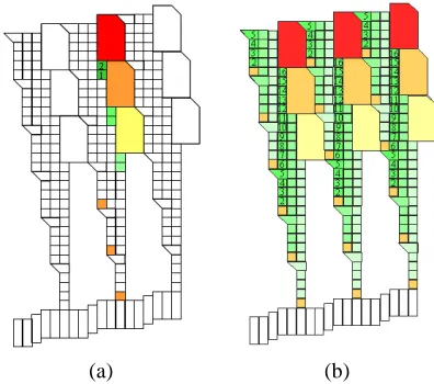
The image capturing operation is shown in Fig. 3. Fig. 3(a) and Fig. 3(b) show the states in which the image signals of the first two frames and of the second to the six-teenth frames are recorded, respectively. In Fig. 3(b), the image signals for the first frame have already been drained to the outside of the sensor through the drain. The image capturing operation with the overwriting continues until the target event occurs and a trigger signal to stop the im-age capturing operation is released to the sensor.
2.2.2 Readout operation
After the image capturing operation ceased, the image signals stored in the in-situ storage are read out to a buffer memory outside the sensor and, finally, reconstructed as consecutive image frames. At first, the image signals stored in the vertical readout CCDs, i.e., the last segments of the storage CCD elements, are readout through the horizontal readout CCDs. When the vertical readout CCDs become empty, the image signals stored in the storage CCD ele-ments are transferred to the vertical readout CCDs until they are filled with the image signals. The operation is re-peated until all the image signals are read out of the sensor
(a) (b)
and the in-situ storage CCDs become empty.
2.3
Test sensor and example image
The first sensor of the ISIS was developed in 2001, named ISIS-V2, and mounted on a camera developed by Shimadzu Corporation [2]. Now the camera is available in market. The very high performance has been proved through applications of the camera to various targets in sci-entific and engineering research and development.
Fig. 4 shows example images of a shock wave re-flected at and transferred through a water surface captured at 500,000 fps. Sound in water propagates much faster than in air as learned from textbooks.
Fig. 4 Shock wave propagation at a water surface. (Captured by Takayama et al with the ISIS-V2 at 500,000 fps)
Fig. 5 Laser ablation of gelatin (10 wt%; water 90 wt%). (Cap-tured with the ISIS-V2 at 250,000 fps)
Fig. 6 A soap bubble (Captured with the ISIS-V4 at 5,000 fps).
Fig. 5 shows ablation from gelatin by a shot of a pulsed laser beam captured at 250,000 fps [5]. The wave length, the pulse width and the energy density of the beam are 10.6 microns, 80 ns and 6.7 J/cm2, respectively.
2.4
Evolution of the ISIS
The ISIS-V2 is a monochrome sensor with the pixel count of only 81,120 (=312×260). The color version with higher resolution with the pixel count of 302,400 (=420× 720) has been developed by NHK (Ohtake, Hayashida et
al., 2006) [6]. The ISIS is continuously being evolved. As
shown in the following sections, currently, the ISIS-V12 with ultra-high sensitivity as well as ultra-high frame rate is under processing, and the ISIS-16M, aiming at 16 Mfps at first and 100 Mfps in the future, is being designed with sacrifice of the dynamic range.
The ISIS concept has been applied to develop novel high-speed image sensors in other organizations. For ex-ample, in the LCFI, the linear collider flavour identifi-cation, a group of scientists are developing a new sen-sor based on the concept (Allport et al., 2005, Stefanov, 2006) [7, 8]. They employed the CMOS readout scheme combined with the ISIS for the storage part for more flex-ible readout after capturing a signal sequence. The combi-nation was proposed by the authors in 2002 (Etoh et al., 2002) [9] and named RA-ISIS, the random-access in-situ storage image sensor.
The evolution process is summarized in Table 1. Ex-ample images of the ISIS-V4, the color and high-resolution version of the ISIS, are shown in Fig. 6.
3. PC-ISIS: Image Sensor with
Ultra-High Speed and Ultra-Ultra-High
Sensi-tivity
3.1
The PC-ISIS
3.1.1 Combined technologies
sen-Table 1 The evolution of high-speed image sensors in Kinki University and NHK.
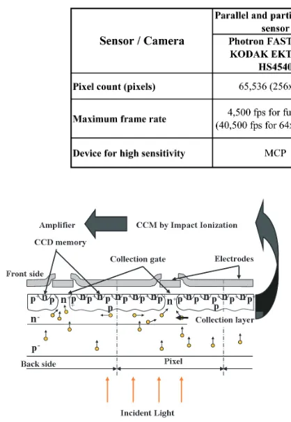
Fig. 7 PC-ISIS: the cross section1-1’ in Fig. 1.
sitivity is also required. The sensitivity of less than 10 photons will be achieved by introduction of three exist-ing technologies: backside-illumination, coolexist-ing, and the CCM, Charge Carrier Multiplication invented by Hynecek (1993) [10].
The sensor under development satisfies both require-ments of the ultra-high speed and the ultra-high sensitivity. The sensor was named the PC-ISIS, the Photon-Counting In-situ Storage Image Sensor.
3.1.2 Cross-section structure
The cross section 1-1’ in Fig. 1 is shown in Fig. 7. The ISIS structure and the CCM are installed on the sur-face of the ISIS. Therefore, the structure of the PC-ISIS is much more complex than that of the standard back-side illuminated CCD. In this figure, arrows express flow of electrons.
In the figure,
(1) Electron-hole pairs are generated in the backside layer by the incident light to the backside of the sensor.
(2) The electrons are transferred to the collection gates through the collection layer, and stored as image signals in the linear CCD channels, which run perpendicularly to the paper surface.
(3) The holes are continuously drained from the sen-sor.
3.2
Pixel structure
The specifications of the pixel and the sensor are sum-marized as follows:
(1) Pixel Size
The length of a CCD cell is 3.6µm. Each pixel con-sists of ten CCD channels, the collection gate and drains for holes and electrons. Each CCD channel has twelve CCD cells. The size of a pixel is the product of the size and the number of CCD cells in one channel, i.e., 3.6µm
×12 elements=43.2µm. (2) Thickness of the chip
To achieve fast electron transfer, the sensor should be completely depleted. Therefore, thinning process is ap-plied to the chip to 24 micron thick.
(3) Pixel count and the size of the chip
The pixel count is 172,800 pixel (480×360). The size of the photo-receptive area is 20.73×15.552 mm2,
calcu-lated by multiplying the pixel size and the pixel count. (4) Number of frames
The number of frames of continuously captured image is 117, which is the same as the number of the CCD storage elements for one pixel.
(5) Sensitivity
With combination of the 100% fill factor by back-side illumination and the amplification by impact ioniza-tion (CCM), the sensitivity is expected to be less than 10 photons for standard readout rate.
Since the PC-ISIS is a backside-illuminated image sensor, it is sensitive to ultraviolet rays and visible light.
On the other hand, infrared ray and some portion of red light penetrate through the 24-micron-thick chip and reach the CCD storage channel made on the surface. There-fore, the sensitive wave length of the sensor is limited up to 600 nm.
(6) Other functions
Overwriting mechanism is installed. Continuous par-allel readout is also possible up to 500 fps.
4. Further Increase of the Frame Rate
4.1
CCD element structure
which results in the lower dynamic range.
Fig. 8 shows the plane structure of the CCD element.
4.2
Sensor structure
Fig. 9 shows the plane structure of the sensor. It has four independent blocks, each with a photo-receptive area, a readout CCD, a CCM, an amplifier and a readout tap. The driving voltage is delivered both from the top and the bottom edges of the sensor.
Fig. 8 The plane structure of the new CCD elements.
Fig. 9 The plane structure of the sensor.
Table 2 The parameters and results of the preliminary simulation.
4.3
Preliminary simulations
4.3.1 Transfer in the collection layer and the theoreti-cal maximum frame rate
Preliminary simulations are conducted by using the parameters shown in Table 2.
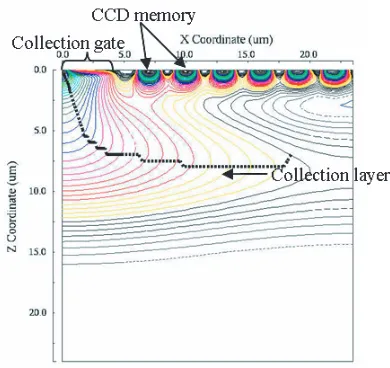
The frame rate is the inverse of the time for an elec-tron to travel from the edge of a pixel to the collection gate through the collection layer, and finally to the input gate. Along the electron path, sufficiently smooth electric field must be realized, as shown in Fig. 10. Even if there is a slight up-and-down or a long flat root in the path, electrons are trapped or detained, which causes serious decrease of the traveling time. To achieve the maximum frame rate, the minimum electric potential gradient (electric field) in the path should be maximized. Extensive simulation study for the pixel of 43.2×43.2µm2and the thickness of 24µm has finally realized that the traveling time through the collec-tion layer is 5.6 ns and that in the colleccollec-tion gate is 0.9 ns; the total is less than 6.5 ns. Therefore, the theoretical max-imum frame rate of this sensor is expected to be more than 100,000,000 fps.
4.3.2 Channel potential and charge handling capacity Preliminary simulations are also conducted to opti-mize the channel potential profile and estimate the charge handling capacity. The charge handling capacity was so far estimated as 3,000 e- for the virtual transfer system and 5,000 e- for the standard two phase transfer system, re-spectively.
5. Sensor with a Large Area
5.1
Technologies to produce large sensors
The ISIS has very large pixels, since many storage el-ements are installed in each pixel, resulting in the relatively small pixel count. Therefore, to increase the spatial resolu-tion of the ISIS, it is required to enlarge the size.Large image sensors are also required in various sci-entific and engineering fields for higher spatial resolution. For example, a standard window size of a TEM is much wider than that of the standard image sensors.
Currently, there are three technologies available to make large-area image sensors as follows:
Fig. 11 ISIS-V4 made by butting [6].
Fig. 12 Terraced image sensor.
(1) Stitching, (2) Butting, and (3) Overlapping. Stitching connects the mask images on a wafer to make an IC chip with a large area. The yield rate of an IC device decreases inversely proportionate to the third to the forth power of the area. Since the chip is processed and diced as one large sensor after stitching on the wafer, the yield rate seriously drops for increasing the area.
Butting pastes medium-size chips on a surface of a package with very small gaps. It has been applied to large-size sensors for astronomy. Usually, one column and/or row between adjacent chips is lost. Fortunately, since the pixel size of the ISIS is very large, butting was success-fully applied to the ISIS-V4 to double the pixel count from 420×360 to 420×720 as shown in Fig. 11 (Ohtake, Hayashida et al., 2006) [6].
An example of overlapping technology is shown in Fig. 12. This is “The Terraced Image Sensor” proposed by Etoh et al. (2002) [11]. The narrow open area of each chip receives the incident light and the other area is used for memories and image signal processing, such as ADC.
5.2
Precision dicing close to the photodiode
To make butting sensors and terraced image sensors, the wafer should be diced very close to the photodiodes.
Fig. 13 shows the diced cross section. The dicing an-gle is slightly larger than 90 degrees for perfect butting. A special dicing machine with slanted saw was introduced. Otherwise, the bottom edges of the chips contact and the top edges have some opening by automatically slightly
Fig. 13 Dicing with a small angle [6].
(a) Dicing lines (b) Leakage
slanting dicing saw of the standard dicing machine. Fig. 14 shows the leak current due to dicing very close to a diode (Ohtake, Hayashida et al., 2006) [6]. If the dis-tance from the edge of the photodiode is larger than 3µm, no leakage appears practically. The critical distance is pos-sibly decreased by removing the surface of the dicing face from which micro cracks may have developed to the depth of three microns.
5.3
Focusing for the terraced image sensor
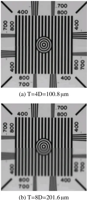
Fig. 16 shows the results of experiments on the depth of focus on two terraced chips with the thickness of 50µm.Commonly, the depth of field is expressed as D=2×(F-value of the optical system)×(pixel size) Generally, if the thickness T of the chip is less than 2D, the incident light image focuses on both of the chip surfaces.
For the experiments, a video camera with a progres-sive CCD image sensor with 1,000×1,000 pixels of the CCD element size of 9.0 ×9.0µm2 is applied. The
F-value is 1.4. Therefore, the depth of field D is 25.2µm
Fig. 15 The test pattern.
Fig. 17 Terraced image sensor for Dynamic TEM. (=2×1.4×9).
The test pattern is shown in Fig. 15.
In the experiments, the camera was slid from the po-sition of the perfect focusing. Fig. 16 shows the perfectly focused images in the upper half of the frame and the de-focused ones in the lower half.
The result showed that if the defocusing distance is less than 100.8µm, i.e., the thickness T is less than 4D, defocusing is negligible, which suggests that the terraced
(a) T=4D=100.8µm
(b) T=8D=201.6µm
image sensor is practical.
Fig. 17 proposes a terraced image sensor for the TEM. The terraced surface is covered with fiber-optics with stepped bottom surface and the flat top surface. The fiber is made of glass doped with thick lead to prevent the CCD from damage due to X rays.
6. Conclusion
Since the early 1990’s, the authors have been engaged in development of high-speed video cameras. This paper summarized the evolution process in the past and the per-spective of the future development.
The maximum frame rate of the currently available cameras is 1 Mfps. Design of the new sensor aiming at 100 Mfps in the future has started.
To achieve 100 Mfps, other supporting technologies should be developed in parallel, which includes a special power circuitry.
The authors sincerely hopes our ultra-high-speed video cameras will contribute to research and development on the plasma physics and engineering.
[1] T.G. Etoh, A high-speed video camera of 4,500 fps, Journal of the Institution of Television Engineers 46 (5), 543 (1992) (in Japanese).
[2] T.G. Etoh et al., A CCD image sensor of 1Mframes/s for continuous image capturing of 103 frames, Digest of Tech-nical Papers, ISSCC 2002, pp.46-47 (2002).
[3] URL http://bionanoscope.web.infoseek.co.jp/eng/index. html
[4] T. Etoh and H. Mutoh, U.S. Pat. No. 6972795B1, High-speed imaging device (2005).
[5] Y. Hashishin et al., unpublished original image.
[6] H. Ohtake, T. Hayashida et al., 300,000-pixel ultrahigh-speed high-sensitivity CCD and a single-chip color camera mounting this CCD, Broadcast Technology, NHK STRL
28, 2 (2006).
[7] P. Allport et al., Linear Collider Flavour Identification: Case for Support, P306/D89506, pp.1-43 (2005).
[8] K. Stefanov et al., Nucl. Instrum. Methods 565 (1), 157 (2006).
[9] T.G. Etoh et al., An in-situ storage image sensor of 1,000,000 fps with slanted linear CCD storage, ITE Tech-nical Report 26 (26), 27 (2002).
[10] Jerry Hynecek, U.S. Pat. No.5,337,340, Charge multiply-ing detector (CMD) suitable for small pixel CCD image sensors (1993).
[11] T.G. Etoh, Progress beyond ISIS: Combined triple-ISIS camera, video trigger and terraced image sensor, Proc. of
25th International Congress on High-Speed Photography

![Fig. 11 ISIS-V4 made by butting [6].](https://thumb-us.123doks.com/thumbv2/123dok_us/8446956.1703579/6.595.350.507.466.585/fig-isis-v-made-by-butting.webp)