Study of the Interconnect Failure Mechanism and
Micro-effort for ULSI
Qian Lin
1, Haifeng Wu
2*1 College of Physics and Electronic Information Engineer, Qinghai Nationalities University, Xining, 810007,
China.
2 Chengdu Ganide Technology, Chengdu, 610073, China.
* Corresponding author. Tel.: 13997266556; email: [email protected] Manuscript submitted March 10, 2019; accepted April 11, 2019. doi: 10.17706/ijcce.2019.8.3.104-118
Abstract: Interconnect reliability has been regarded as a discipline that must be seriously taken into
account from the early design phase of ultra large scale integration (ULSI). A synthetic review of valuable solutions to improve interconnect reliability is proposed in this paper. At first, a comprehensive review of the interconnect failure mechanisms and micro-efforts are carried out. Four types of interconnect failure mechanisms including EM, SM, TM and TDDB are illustrated in detail. Depending on their different effects for failure, the interconnect micro-effects are classified into the positive effects including the short-length effect, self-healing effect, reservoir effect and the negative effects which involves the skin effect, joule heating, current crowding , bandwidth, coupled noise, parasitic, RC delay, crosstalk and power dissipation and so on. Secondly, a novel qualitative evaluation method based on the radar chart has been presented, which visually shows the contrast of the key performance related to the interconnect failures. These present results might provide some valuable guidance for the study of IC interconnect reliability.
Key words: Ultra large scale integration (ULSI), electromigration, interconnect reliability, RC delay, failure
mechanisms, micro-effects.
1.
Introduction
crosstalk and noise cannot be neglected and become the new challenges for interconnect reliability [3]. In this case, the main interconnect failure mechanisms and micro-effects are summarized here, which are closely related to some factors such as current density, temperature, width and so on. In order to evaluate the interconnect reliability, how to measure the impacts of failure mechanisms, micro-effects and the related factors on interconnect reliability should be considered. Furthermore, a novel qualitative evaluation method has been presented, which show their influences on interconnect reliability visually. This paper is arranged as following, the failure mechanisms and micro-effects have been summarized in Section II. A novel method to evaluate the interconnect reliability is presented in Section III. Finally, the conclusion is given in the Section IV.
2.
Interconnect Failure Mechanisms and Micro-effects
With the advent of nanometer era, it needs large quantity of complex interconnects to connect highly integrated chip with the other electronic components. In view of the above-mentioned, interconnect reliability must be addressed. In order to analysis the interconnect reliability, it is extremely necessary to find out the reasons and influence factors for the IC interconnect failure. In this part, the failure mechanisms and micro-effects of interconnect are analyzed. One of the goals is to identify the failure mechanisms and their impacts on the interconnect properties.
(a) The number of papers for failure mechanisms (b) The paper distribution of failure mechanisms Fig. 1. The statistic for interconnect failure mechanisms.
2.1.
Interconnect Failure Mechanisms
With the increase of failure rate, to identify the failure mechanism is the key to ensure reliability. There are mainly four types of interconnect failure mechanisms [4] including EM, SM, TM and TDDB. The paper statistic is investigated in Fig. 1(a) and (b), which indicates that EM is the most significant threat for interconnect reliability in the high performance IC.
2.1.1. EM failure
EM is a complex multi-physics problem including electrical, thermal and mechanical. Since EM failure had been found in the 60’s, research on EM has progressed significantly and the physics theory was well established. The first report on EM was presented by Fiks in 1959 [9]. Then, Huntington and his coworkers contributed to EM failure and proposed that electron wind force was taken as the only driving force for EM mass transport [10]. The reduction in line width and the increase of temperature gradient which is caused by the changes of temperature and mechanical stress gradient are the major reasons for EM [11]. Tan investigated the influence of temperature and stress gradient for the Cu narrow interconnect [12]. Then Arzt and Kraft studied the effect of surface tension gradient in EM. Later, Dalleau combined these driving forces to analysis EM in Al considering voids dynamic growth [13]. The work by Li showed that current density was no longer the sole driving force for EM when the line width became less than 0.20μm.
EM failure is generally described by the famous Black equation which is used to determine the maximum current density flowing in a wire safely. In 1969, Black proposed the classic EM failure time formula, it can be written as equation (1) [14], where A is a constant based on interconnect geometry and material, j is the current density, Q is the activation energy (0.5eV for Cu and Al alloys), KB is the Boltzmann constant and T is
the temperature. 2 exp B Q MTF Aj K T
(1)
From the equation (1), it can be observed that the meantime to failure ( ) of interconnect decreases exponentially with the increase of temperature [15
interconnect lines and becomes the typical lifetime assessment method now.
Cu EM and Al EM are significantly different due to their different architectural schemes. While the EM in Al interconnects was well studied. It was found that EM in Al was caused by the diffusion of grain boundary in the 1960s [16]. Under the higher current density, metal ions of interconnect film are prone to spread and diffuse, especially in metal wire with the bamboo structure. It is reported that failure rate caused by EM is extremely high after 0.18um technology node in Al [17]. Nowadays, EM can be predicted by combing the FEA and ANN techniques for ICs [18], [19]. In addition, the introduction of new materials and processing schemes leads to even more challenges in guaranteeing interconnect robustness.
2.1.2. SM failure
Except for EM, the stress-induced-voiding (SIV) or SM is the major failure mechanism which is the result of vacancy movement due to the stress gradient [20]. The stress gradient is the driving force for vacancy diffusion that contributes to the void growth. When interconnect line is placed in the condition of high temperature or no electricity, open circuit is formed by the growth of void and the increase of interconnect resistance [21]. It has been found that large stress builds up and results in the difference of CTE between the metal lines and surrounding dielectrics. The change of temperature in the manufacturing or baking process would form vacancy or cavity nucleation and make the residual thermal stress existed in interconnect system. Areas with the concentrated stress are thought to be the probable spots where voids nucleate. Moreover, the space or hollow is formed along the direction of stress gradient. Generally, SIV occurs at the metal/dielectric interface or via, depending on the properties of the material, geometrical and other aspects related to process.
2.1.3. TM failure
The elevated temperature is the major contributor for reliability degradation. In the micro-interconnect structure, high current which is caused by the geometrical shape of interconnect lines would produce a large number of joule heating and local temperature rise and even temperature gradient. The temperature gradient brings about TM which occurs along the direction of temperature gradient [22]. It is investigated
MTF
that the thermo-mechanical stress is the dominant factor and can’t be ignored when the line width is below 200 nm. It is reported that TM is found to be the key failure in the 3D interconnect.
2.1.4. TDDB failure
The TDDB failure in the Cu/ULK interconnect stacks has become one of the most critical reliability issues for state-of-the-art interconnect dielectrics in recent years. TDDB has never been an issue for the Cu/SiO2 interconnects, but when the dimension is below 90 nm, it has become the most serious reliability challenge. TDDB failure is the breakdown related to dielectric materials and time in interconnect system [23]. It is a wear-out of dielectric caused by the electric field and temperature. Under the action of electric field, the drift of Cu ions in dielectric layer directly produces TDDB failure. Extensive efforts are made to solve this issue and several models have been proposed to describe the relationship between electric field and lifetime. Chen did research on TDDB failure and reliability lifetime model for Cu interconnect [24]. Because of the different properties of Cu and Al, the Cu interconnect with barrier layer would bring prominent differences from the Al without barrier layer in TDDB degradation. Due to the decrease of intrinsic breakdown strength of dielectric material, TDDB failure has received extensive concern now.
2.2.
Interconnect Micro-effects
The lifetime is the important index to signify the interconnect reliability. With the reduction of feature size and the improvement of working frequency, it is vital to emphasize the interconnect micro-effects which directly influence the interconnect lifetime [25]. For instance, as the operating frequency continues to spiral upward, the interconnect parasitic effect must be considered, which is caused by the increase of interconnect resistivity and capacity. In additional, the problems of delay, power dissipation, bandwidth and noise become more stringent [26].
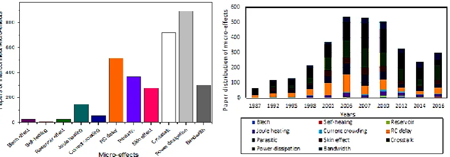
In addition, a comprehensive analysis of the interconnect micro-effects is given and the paper distribution is illustrated in Fig. 2 (a) and (b). It indicates that parasitic, RC delay, crosstalk and power dissipation have attracted more attention nowadays. Depending on their different effects for failure, these micro-effects are classified into the positive effects and the negative effects.
(a)Nnumber of papers for interconnect micro-effects (b)Paper distribution of interconnect micro-effects Fig. 2. The statistic of interconnect micro-effects.
2.2.1. Positive effects
A. Short-length effect (blech effect)
difference of hydrostatic stress at anode and cathode, *
Z is the effective charge of the Cu, is the resistance of metal, q is the charge of metal, Ω is the atomic volume.
*
(jL)Blech
Z q
(2)
It means that when the product of conductor length (L) and void density (j) is less than a certain threshold, no EM occurs. It has found that shorter Al wires are substantially less susceptible to the EM damage than longer lines when stressed under the same condition [28]. The short-length effect in the DD Cu interconnects has been investigated through the experiments on the lines of different lengths, different current densities in the three-level structure [29].
The product (jL) Blech is determined by the varying metal length and current density [30]. Fig. 3 depicts the decreasing tendency of (jL) Blech with the failure rate, which means that the reliability is improved by (jL) Blech. Moreover, short-length effect has a profound impact on increasing current limit and brings long EM lifetime. In general, jL/B (B is the effective Bulk Modulus) is used as a figure of merit to describe immortality of interconnect lines. However, jL2/B is the correct figure of merit [31]. Therefore, as an accelerated EM factor, (jL)
when it reaches a certain value.
Fig. 3. The trend of (jL)Blech vs. failure rate [30].
B. Self-healing effect (back-flow effect)
EM can cause atomic directed movement then form gradient concentration. Because of the existence of mass gradient, the phenomenon of atoms redistribution is called self-healing or back-flow effect which can reduce EM and repair the EM defects. Because the change of materials is inevitable, so the repair is incomplete. In the case of alternating current or pulse, self-healing effect improves the EM lifetime and is benefit to interconnect reliability [32].
C. Reservoir effect
Reservoir effect means that the part area of metal provides a large number of metal ions which likes an ion library. It is available to fill the missing ions in contact or near vias during EM [33]. In order to compensate the metal ions which are stopped near the borders by the electronic wind migration, it is necessary to control the via formation and expansion. The reservoir area is consisted of the top cap, via area and end lap in MLI structure. It is defined as an extended region of metal line under or over vias.
as the line extension part serves as reservoir of atoms during EM. Nguyen explored the effect of reservoir area on the EM reliability using Al and Cu interconnect respectively [34]. The results reflected the dependency of median time to failure (MTTF) was on the total reservoir area rather than the via pattern. It is reported that the reservoir slows down EM failure and prolongs the interconnect lifetime but up to a certain extend beyond which there is no improvement. Generally, reservoir effect is benefit to improve the interconnect reliability.
2.2.2. Negative effects
A. Skin effect
High density integration makes the conditions of heat dissipation deteriorated constantly. Especially in the signal lines of high frequency, the influence of skin effect is indispensable. The skin effect refers to the exponential reduction of current density along the direction of conductor center and the total current distribution can be equivalent to uniform current distribution in metal layer with a thickness of delta (δ). When the frequency exceeds the certain value, skin effect will occur. A self-consistent method to guide the reliability design of high frequency for a two-level Cu interconnects incorporating the impact of skin effect was presented in [35]. The main intention is to analyze the impact of the signal attenuation induced by skin effect.
B.
Joule heating effect (self-heating effect)
As the scaling of IC and the increase of current density, Joule heating has received tremendous attention in interconnect. The impact of Joule heating in metal lines becomes an unavoidable problem. Joule heating which is also named as self-heating is depended on the factors such as current density, interconnect resistivity, ambient temperature, surrounding materials and interconnect design. For example, the metal/Si contacts and inter-layer vias often bear extremely high current density and Joule heating. In the process of signal transmission, the impact of thermal performance cannot be ignored when current flows through the interconnect lines. The heat of the top interconnect is difficult to dissipate and would induce failure. And the Joule heating of the Cu wires can be expressed as equation (3):
2
S
QI (3)
where Q is the Joule heating, ISis the current density in Cu lines, is the resistivity of Cu. The rise of
temperature and temperature gradient caused by Joule heating has significant influence on the IC reliability. In reference [36] showed the effect of self-heating based on a 4-level interconnect test structure and presented a thermal simulator for the design process. Moreover, it is found that non-uniform current distribution introduces higher power density than the uniform one near contacts. Joule heating also strongly impacts the power dissipation of interconnect which is the another challenge for the complicated IC.
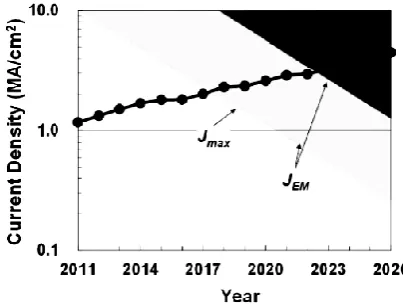
C. Current crowding effect
Fig. 4 shows that current crowding has become remarkable with the improvement of technology. With the increasing current density, the current crowding and current gradient indeed exist in the angled structure. When the current crowding occurs in the Cu and interfaces of barrier layer, EM is intensified. In order to relieve current crowding, the interconnect optimal design is the best choose [37]. Kwok [38] did the pioneer attempt to understand the current distribution in two-level studs and vias. They used the two-dimensional FEM simulation to calculate the distribution of current and temperature in MLI.
Fig. 4. The general trend of current density.
D. Interconnect parasitic effect
As the increase of interconnect density, interconnect parasitic effect has become the major restrictive factor for realization of high speed, high density, low power consumption, multi-function of IC. The capacitance is the dominant contribution to the parasitic effect and limits the speed of circuit directly. Therefore, in order to reduce the cross-section area of interconnect is the most beneficial measure. In addition, the exploration of new material is inevitable to reduce parasitic effect. For instance, Cu is used to reduce the interconnect resistance and low-k is used to reduce interconnect capacitance. Another method is to analyze the parasitic effect based on some parasitic models. How to build the precise and effective interconnect parasitic model has become the focus for interconnect design. In addition, the inductive effect began to be highlighted in the distributed RLC equivalent circuit model with the nano-scale CMOS process.
E. RC delay
In parallel, the interconnect delay is becoming the limitation of the overall signal propagation. The total resistance (R) of the interconnect structure is now a significant factor affecting the chip performance. At the same time, the capacitance (C) between wires is increasing due to the decreasing spacing between wires. Both factors significantly increase the RC delay of IC. Nowadays, the limitation to IC reliability is not the gate delay of device, but the interconnect delay which is caused by the parasitic components. The interconnect resistance and capacitance between metal layers are the major parasitic components, which directly decide the RC delay. That is to say by reducing total resistance and capacitance can decrease the interconnect delay. The RC delay in interconnect wires can be calculated by the equation (4) as follow:
2
0 2 2
1 1
2 ( )
delay
RC k L
W T
(4)
where L is the length of interconnect line, T is the height of metal, W is the thickness of metal, ρ is the resistance of metal, k is the dielectric constant, 0is the dielectric constant of vacuum. When the working
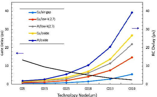
Fig. 5. Gate delay and interconnect delay versus year.
RC delay severely impacts the interconnect performance. Therefore, it is necessary to take measures to optimize delay. It is reported that the efficient methods to reduce RC delay include using low-k dielectric, inserting repeater and increasing line width [39]. The first approach to reduce interconnect delay is to improve the interconnect materials. The silicate and Cu can help to reduce resistance of polycrystalline silicon and metal wire. Low-k dielectric is used to reduce capacitance. It is widespread to use the Cu and low-k in advanced CMOS process. As the Fig. 6 shown, different interconnect structures have different RC delay and gate delay, especially the Cu/air-gap structure has the lowest RC delay. However, the new materials generally can keep only one or two generations, delay has not been solved thoroughly. To update technology is the only way to deal with the delay.
Fig. 6. Gate delay vs. RC delay in different interconnect structures.
Fig. 7.The delay for local and global gate delay with/without repeater.
F. Crosstalk and coupled noise
When the peak value of interference noise induced by the electromagnetic coupling between the adjacent lines is big enough, logic chaos of transmission signal occurs and makes the terminal load out of order [40]. The crosstalk and coupled noise are the potential failure in high speed electronic system. What is more, crosstalk would change effective characteristic impedance and system delay. Meanwhile, the signal integrity is also destroyed by the crosstalk and noise.
G. Interconnect power dissipation
With the tendency of miniaturization and function integration, the interconnect density and power dissipation increase obviously. Circuit designers must minimize the parasitic capacitance to reduce the power dissipation and improve circuit speed. In 2012, ITRS pointed out that the layer number of interconnect has reached 13, interconnect length of IC has accumulated up to 103 m, while the power dissipation of individual IC continues to increase [41]. It indicates that power dissipation has become new focus for interconnect reliability. In addition, interconnect power dissipation increases greatly and occupies a large proportion of the whole power dissipation. It directly impacts the integration and reliability of the system.
Fig. 8. The trend of dynamic power dissipation.
H. Interconnect bandwidth
The bandwidth is the amount of data which is transmitted in chip per unit time. For a given chip, the interconnect bandwidth is the function of unit delay and the number of interconnect and it is given by the equation (5):
1
( )Ttotal
W S
L
(5)
where is the interconnect bandwidth, W is the line-width, S is the line thickness, L is the line length, T
total is the total delay time. Due to the increase of signal frequency, the improvement of bandwidth has become the important part for high speed IC. The target of interconnect design is to obtain larger bandwidth and keep acceptable delay of unit length as far as possible. The large bandwidth means big data throughput and the small delay means high performance interconnect. To increase line width and line spacing is effective to reduce delay at the expense of part bandwidth. They can’t reach the optimal value at the same time and need to make the reasonable compromise.
2.3.
Evaluation Method
How to evaluate these failure mechanisms and micro-effects in interconnect reliability? Various factors ought to be taken into account, such as the current density, frequency, resistance, capacitance, width and temperature and so on.
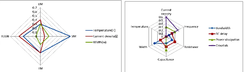
In general, the interconnect micro-effects is divided into two sets, which are related to performance failure and physics failure. The RC delay, crosstalk, power dissipation and bandwidth belong to the physics failure, while Joule heating, current crowding, parasitic effect and skin effect belong to the performance failure. It is reported that current density, temperature, frequency, width, resistance and capacity are the key factors to decide these micro-effects. In order to evaluate the extent, a novel qualitative evaluation method has been put forward-radar chart. Every radial axis represents a performance index and the distance represents the extent of impact.
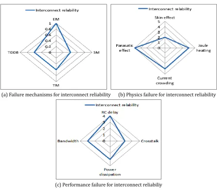
Take the failure mechanisms for example, by scoring for the factors according the extent of impact. The radar chart is as the Fig. 9 and 10 shown respectively, the longer the wire, the greater the impact. From the Fig. 9 (a) we can see that temperature is the major impact and width is the minimum impact for failure mechanisms. From the Fig. 10 (a), it is found that EM accounts for the maximum proportion for interconnect reliability.
(c) The factor distribution of physics failures
Fig. 9. Key influences on failure mechanisms and micro-effects.
(a) Failure mechanisms for interconnect reliability (b) Physics failure for interconnect reliability
(c) Performance failure for interconnect reliabiliy
Fig. 10. The influence distribution of failure mechanisms and micro-effects for interconnect reliability.
In the case of micro-effects, the radar chart is as Fig. 9 (b) and (c) shown, the longer the wire, the greater the impact. From the Fig. 9 (b) and (c) we can see that impact distribution for the performance failure and physics failure. From the Fig. 10 (b) and (c) it is shown that parasitic effect and RC delay account for the maximum proportion for interconnect reliability.
interconnect structure the process changes are of crucial importance. Therefore, the interconnect modeling and the process changes need to be taken into account in the interconnect challenges. According to the figures above, we can clearly identify the impact of failure mechanisms or micro-effects for the interconnect reliability. When certain factor varies, it is easy to trace the related failure mechanisms or micro-effects. In turn, when failure occurs, we can quickly pay attention to the certain factors. It is effective to find the reasons for any failures. All these can give some guidance to control failures.
3.
Conclusion
An overview of IC interconnect reliability has been presented. In general, the failure mechanisms and micro-effects for interconnect are analyzed and summarized here. Moreover, a novel qualitative evaluation method has been presented, which visually show the contrast of these failure mechanisms and micro-effects.
With the development of semiconductor industry, the technical and physical extremity would be broken by exploring new materials and new technologies. Moreover, the interconnect parasite, crosstalk noise and RC delay have become the most difficult challenges for IC. All these can provide some valuable guidance for the study of IC interconnect reliability.
Acknowledgment
This work was supported in part by the National Natural Science Foundation (6184110), the Applied Basic Research Plan of Qinghai (2017-ZJ-753), the High-level talent program of Qinghai University for Nationalities (2017XJG04).
References
[1] Srinivasan, J., Adve, S. V., Bose, P., & Rivers, J. A. (2004, July). The impact of technology scaling on lifetime reliability. Proceedings of theInternational Conference on Dependable Systems and Networks (pp. 177-186).
[2] Schaller, R. R. (1997). Moore’s law: Past, present and future. IEEE Spectrum, 34(6), 53-59.
[3] Ekekwe, N. (2010). Power dissipation and interconnect noise challenges in nanometer CMOS technologies. IEEE Potentials, 29(3), 26-31.
[4] Liu, X. Y., Shao, J., Wang, Y., & Zeng C. H. (2011, May). Research on failure modes and mechanisms of integrated circuits. Proceedings of the IEEE Prognostics and System Health Management Conferenced (pp. 1-3).
[5] Oates, A. S., & Lin, M. H. (2009). Electromigration failure distributions of Cu/low-k dual-damascene vias: Impact of the critical current density and a new reliability extrapolation methodology. IEEE Trans
Device Mater Rel., 9(2), 244-254.
[6] Croes, K., Wu, C., Kocaay, D., Bömmels, J., & Tőkei, Z. (2015, May). Reliability mechanisms and lifetime extrapolation methods for scaled interconnect technologies. Proceedings of the IEEE International
Interconnect Technology Conference and Materials for Advanced Metallization (pp. 295-298).
[7] Zheng, H., Yin, B. F., Chen, L. G., et al. (2018, March). Changeable electromigration failure mode in wide Cu interconnects. Proceedings of theChina Semiconductor Technology International Conference (CSTIC)
(pp. 1-3).
[8] Moreau, S., & Bouchu, D. (2013, April). Reliability of dual damascene TSV for high density integration: The electromigration issue. Proceedings of the IEEE International Reliability Physics Symposium (IRPS)
(pp. CP.1.1-CP.1.5).
14-28.
[10] Duryea, T. W., & Huntington, H. B. (1988). The driving force for EM of an atom adsorbed on simple metal surface. Surface Science, 19(2), 261-281.
[11] Anthony, S. O. (2016, May). Interconnect reliability challenges for technology scaling: A circuit focus.
Proceedings of the IEEE International Interconnect Technology Conference/Advanced Metallization
Conference (IITC/AMC) (pp. 59-60).
[12] Tan, C. M., & Roy, A. (2006). Investigation of the effect of temperature and stress gradients on accelerated EM test for Cu narrow interconnects. Thin Solid Films, 504(1-2), 288-293.
[13] Dalleau, D., & Weide-Zaage, K. (2001). Three-dimensional voids simulation in chip metallization structures: A contribution to reliability evaluation. Microelectron. Reliab., 41(9), 1625-1630.
[14] Black, J. R. (1969). Electromigration-a brief survey and recent results. IEEE Trans. Electron. Dev, 16(4), 338-347.
[15] Li, W., & Tan, C. M. (2011, Nov.). Black's equation for today's ULSI interconnect EM reliability-A revisit.
Proceedings of the International Conference of Electron Devices and Solid-State Circuits (pp.1-2).
[16] Blech, I. A. (1976). Electromigration in thin aluminum films on titanium nitride. J. Appl. Phys., 147(4), 1203-1208.
[17] Tan, C. M., Zhang, G., & Gan, Z. (2004). Dynamic study of the physical processes in the intrinsic line electromigration of deep submicron copper and aluminum interconnects. IEEE Trans. Device Mater Rel.,
14(3), 450-456.
[18] Lin, Q., Fu, H. P., He, F. F., & Cheng, Q. F. (2016). Interconnect reliability analysis for power amplifier based on artificial neural networks. Journal of Electronic Testing Theory and Applications, 32(4), 481-489.
[19] Lin, Q., Fu, H. P., Na, W. C., He, F. F., Li, X., et al. (2016). Interconnect reliability analysis of ULSI using automated model generation algorithm. International Journal of RF and Microwave Computer-Aided
Engineering, 26(6), 481-488.
[20] Hauschildt, M., Hennesthal, C., Talut, G., Aubel, O., Gall, M., Yeap, K. B., & Zschech, E. (2013, April). Electromigration early failure void nucleation and growth phenomena in Cu and Cu (Mn) interconnects.
Proceedings of the IEEE International Reliability Physics Symposium (IRPS) (pp. 2C.1.1-2C.1.6).
[21] Gavin, D. R., Derryl, D. J., & Allman, D. (2015, April). An evaluation of accelerated failure time models of stress-migration and stress-induced voiding failures under vias. Proceedings of the IEEE International
Reliability Physics Symposium (pp. 2D.3.1-2D.3.6).
[22] Yao, W., Justison, P., & Poppe, J. (2013, Aug.). Stress-induced-voiding risk factor and stress migration model for Cu interconnect reliability. Proceedings of the IEEE International Reliability Physics
Symposium (IRPS) (pp. 2C.5.1-2C.5.8).
[23] Patra, S., Chen, D., & Geiger, R. (2012, Aug.). Reliability modeling of metal interconnects with time-dependent electrical and thermal stress. Proceedings of the IEEE 55th International Midwest
Symposium on Circuits and Systems (MWSCAS) (pp. 514-517).
[24] Lin, M., Liang, J., Juan, A., & Su, K. C. (2013, July). Electrical properties of low-k dielectric in copper interconnect structures. Proceedings of the 20th IEEE International Symposium on the Physical and
Failure Analysis of Integrated Circuits (IPFA) (pp. 208-211).
[25] Xia, F., He, J., Prabhumirashi, P., Schmitz, A., Lowrie, A., Hicks, J., Shusterman, Y., & Brain, R. (2011, April). Characterization and challenge of TDDB reliability in Cu/low K dielectric interconnect. Proceedings of
theInternational Reliability Physics Symposium (pp. 2C.1.1-2C.1.4).
International Reliability Physics Symposium (pp. EM.2.1-EM.2.6).
[27] Sakurai, T. (1993). Closed-form expressions for interconnection delay, coupling, and crosstalk in VLSI.
IEEE Trans Electronic Device, 40(1), 118-124.
[28] Manning, K. (2012, Oct.). The application of a modified Blech product to aluminum-based metallization for increased current density. Proceedings of the IEEE International Integrated Reliability Workshop
Final Report (IRW), (pp. 129-131).
[29] Oates, A. S. (2013, June). The electromigration short-length effect and its impact on circuit reliability.
Proceedings of the IEEE International Interconnect Technology Conference (pp. 1-3).
[30] Li, B. Z., Christiansen, C., Burke, C., Hogle, N., & Badami, D. (2013, April). Short line electromigration characteristics and their applications for circuit design. Proceedings of the IEEE International Reliability
Physics Symposium (pp. 2.1-2.5).
[31] Hau-Riege, S. P. (2002). Probabilistic immortality of Cu damascene interconnects. Journal of Applied
Physics, 91(4), 2014-2022.
[32] Cheng, Y. Q., Todri-Sanial, A., Yang, J. L, & Zhao, W. S. (2016). Alleviating through-silicon-via electromigration for 3-D integrated circuits taking advantage of self-healing effect. IEEE Transactions
on Very Large Scale Integration (VLSI) Systems, 24(11), 3310 - 3322.
[33] Chen, X. M., Gao, G., Geng, B. L., & Li, S. S. (2017, Oct.). Impact of side reservoir on electromigration of copper interconnects. Proceedings of theInternational Conference on Electron Devices and Solid-State
Circuits (EDSSC) (pp. 1-2).
[34] Guan, Z., & Marek-Sadowska, M. (2016, May). AFD-based model of EM lifetime and reservoir effect.
Proceedings of the IEEE International Interconnect Technology Conference/Advanced Metallization
Conference (IITC/AMC) (pp.206-208).
[35] Yao, M., Zhang, X. L., Zhao, C. Y., & Ma, J. G. (2011). Self-consistent design issues for high frequency Cu interconnect reliability incorporating skin effect. Microelectronics Journal, 51(5), 1003-1010.
[36] Croes, K., Li, Y., Lofrano, M., Wilson, C. J., & Tőkei, Z. (2013, April). Intrinsic study of current crowding and current density gradient effects on electromigration in BEOL copper interconnects. Proceedings of
theIEEE International Reliability Physics Symposium (IRPS) (pp. 2C.3.1-2C.3.4).
[37] Kim, A., Li, B. Z., & Linder, B. (2018, March). Transient self-heating modeling and simulations of back-end-of-line interconnects. Proceedings of the IEEE International Reliability Physics Symposium
(IRPS) (pp. P-MR.2-1-P-MR.2-5).
[38] Kwok, T., Nguyen, T., Ho, P., & Yip, S. (1987, April). Current density and temperature distributions in multilevel interconnection with studs and vias. Proceedings of theIEEE International Reliability Physics Symposium
[39] Shi, F., Wu, X. B., & Yan, Z. Y. (2014). Improved analytical delay models for RC-coupled interconnects.
IEEE Transactions on Very Large Scale Integration (VLSI) Systems, 22(7), 1639-1644.
[40] Matthew, S., Halligan, D., & Beetner, G. (2014). Maximum crosstalk estimation in lossless and homogeneous transmission lines. IEEE Transactions on Microwave Theory and Techniques, 62(9), 1953-1961.
[41] Kazerooni, M., Cheldavi, A., & Kamarei, M. (2010). Crosstalk and electromagnetic interference noise investigation for a coupled pair of microstrip lines with a break in ground structure. IET Microwaves,
Antennas & Propagation, 4(9), 13364-1346.
[42] Jiang, L. L., Cheng, Y. H., & Mao, J. F. (2010). Analysis and optimization of thermal-driven global interconnects in nanometer design. IEEE Transactions on Components, Packaging and Manufacturing
Technology, 1(10), 1564-1572.
Qian Lin received the Ph.D. degree in circuits and systems with Tianjin University in 2017, Tianjin, China. She is currently an associate professor in Qinghai University for nationalities. Her research interests include the modeling and simulation of IC reliability.
Haifeng Wu has received the BE and ME degrees in electronics from University of
![Fig. 3. The trend of (jL)Blech vs. failure rate [30].](https://thumb-us.123doks.com/thumbv2/123dok_us/1310693.1638649/5.595.183.411.353.512/fig-trend-jl-blech-vs-failure-rate.webp)