IMPLEMENTATION OF
COMPLEMENTARY PASS TRANSISTOR
LOGIC FOR LOW POWER MULTIPLY AND
ACCUMULATE CIRCUIT
Y. JYOTHI M.Tech.
Assistant Professor, Department of ECE, Baba Institute of Technology and Sciences Visakhapatnam,Andhra Pradesh, Pin code: 500048, INDIA
E-mail: [email protected]
G. ASWAN KUMAR M.Tech.
Assistant Professor, Department of ECE, Baba Institute of Technology and Sciences Visakhapatnam,Andhra Pradesh, Pin code: 500048, INDIA
E-mail: [email protected]
S. SINDU BHAVANI M.Tech scholar,
Assistant Professor, Department of ECE, Baba Institute of Technology and Sciences Visakhapatnam,Andhra Pradesh, Pin code: 500048, INDIA
E-mail: [email protected]
ABSTRACT:
A high-speed with a low-power logic circuit technique, is used for many VLSI applications. An SRPL i.e., Swing restored pass-transistor logic network which is introduced here in this paper is used to perform logic evaluation. And additionally, to drive gate outputs, a latch-type swing restoring circuit is used. This technique renders a very high circuit performance. In this paper, we use an SRPL based multiply and accumulate circuit (MAC) for multimedia applications and this is implemented using double metal 0.4micron CMOS technology.
Keywords: SRPL (Swing Restored Pass Transistor Logic), MAC (Multiply and Accumulate Circuit), 0.4Micron
CMOS
1.INTRODUCTION
In the development of microelectronic technologies, the demand for electronic circuits with extremely low supply voltages as well as low power consumption is very important. Additional requirements such as more speed in operation performance and accuracy of signal processing became necessary requirements in many applications.
The fulfillment of the above mentioned demands is not so easy and appears to be problematic. Since the last two decades, the signals representing information are in the form of electric voltages and currents as a result of the evolution of new applications of Digital signal processing.
For any digital signal processing or control system, the fundamental operation would be Multiplication. The speed and accuracy of a digital system depends upon the performance of the resident multipliers. Another important component in digital system is an adder as they are extensively used in other arithmetic operations such as subtraction, multiplication and division. Hence, for the advanced execution of binary operations inside a circuit compromised of such blocks, the digital adder’s performance should be improvised. The performance of a digital circuit block can be known by analyzing its parameters like power dissipation, the layout area and its operating speed.
technology could not improve the battery storage capacity not much than 30% for every five years, which is not at all sufficient to handle the increasing power requirements of portable systems. Low-power devices are expected to have small battery size, less weight, and long lifetime of the battery.
Though the power dissipation criteria are important for portable devices, the operation speed performance continues to be the main goal for digital designers. Consumers expect higher speed, more functionality and higher levels of integration from their cellular phones and other hand-held devices. To emphasize the importance of speed, researchers use energy delay product as an evaluation figure for digital systems. At the same time, reduction in the power dissipation should not come at the expense of speed performance. Increasing the performance while keeping the power dissipation constant is also considered to be one of the low-power design problems.
A major research problem for many years is the designing of low-power circuits with CMOS technology. Several logic families have been proposed and used to improve circuit performance which is much better than that of the conventional static CMOS family. High speed circuit families are becoming attractive in deep submicron technologies since the performance results obtained from the process scaling are decreasing as the feature size decreases.
In the design of multipliers, low power requirement is a challenging task. VLSI designers have different options to reduce the power dissipation in various design stages. The best approach is the Supply voltage scaling because it reduces switching activities and active power but it has the disadvantage of degrading the performance and robustness.
The restrictions the multiplier has to satisfy the area, power and speed requirements. 2. Different Logic Techniques
2.1 Pass-transistor logic:
Pass transistor logic (PTL) describes several logic families which are used in the design of integrated circuits. By eliminating the redundant transistors it reduces the number of transistors used to make different logic gates. Transistors are used as switches to pass logic levels between nodes of a circuit, rather than switches which are connected directly to supply voltages. The number of active devices can be reduced using this type of method but it is disadvantageous in one way because the output levels can be no higher than the input level. Each transistor in series has a lower voltage at its output when compared to its input. If several devices are connected in series in a logic path, then a conventional gate should be constructed to restore the signal voltage to its full value. However, the conventional CMOS logic always switches transistors to the power supply rails so that the logic voltage levels in a sequential chain do not decrease. Since there is less isolation between the input signals and the outputs, designers must take care to assess the effects and consequences of unintentional paths within the circuit. The design rules restrict the arrangement of circuits to avoid sneak paths, charge leakage and slow switching for a proper operation. To ensure adequate performance, simulation of circuits is necessary 2.2 Double Pass Transistor Logic:
Double-pass transistor logic has very limited capacity to drive a load but it eliminates some of the inverter stages required for complementary pass transistor logic by using both N and P channel transistors, with dual logic paths for every function. It has high speed due to low input capacitance.
2.3 Complementary Pass Transistor Logic:
Complementary pass-transistor logic (CPL) or "Differential pass transistor logic" refers to a logic family which is designed for specific advantages. Multiplexers and latches use this logic family for many purposes.
2.3.1. CIRCUIT DESIGN OF CPL:
2.3.2 OUTPUT WAVEFORM FOR FULL ADDER CPL:
(CPL) uses a logic network and CMOS inverters for the driving of the outputs. If the soft pull-up latch is not used, this arrangement can have leakage current through the inverter. Double pass-transistor logic (DPL) uses both PMOS and nMOS devices in the pass-transistor network to avoid non full swing problems. However, it has high area and high-power drawbacks.
Differential cascode voltage switch with pass gate (DCVSPG) is similar to the cascode voltage switch logic proposed. But, it shortens the stack height by the use of a pass-transistor network for logic evaluation and introduces a symmetrical logic topology in the true and complement logic evaluation trees. When used in a long chain without intermediate buffering, this logic style can have degraded pull-down performance. Hence, to avoid the drawbacks of these four logic techniques we now choose for the Swing restored pass-transistor logic (SRPL).
3.SWING RESTORED PASS-TRANSISTOR LOGIC: 3.1 Basic circuit
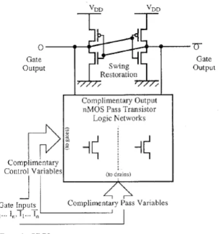
The generic SRPL gate consists of two main parts as shown in the above Figure. A complimentary output pass-transistor logic network is constructed of n-channel devices and a latch-type swing restoring circuit consists of two cross-coupled CMOS inverters. The gate inputs are of two types- the first one is the pass variables that are connected to the drains of the logic network transistors and the second one is the Control variables that are connected to the gates of the transistors.
The logic network has the ability to implement any random Boolean logic function. For instance, the above figure shows the implementation of an SRPL full adder. The swing restoration circuit restores the complimentary outputs of the pass-transistor logic network to full swing.
4. MULTIPLY AND ACCUMULATOR CIRCUIT
Fig. Multiply and accumulate circuit
4.1 MAC Architecture:
It has a 16 bit wide multiplier and multiplicand whereas the accumulated Result has a bit width of 32. The frequency of operation was expected to be more than sufficient to cover even the most advanced multimedia applications and hence a pipelined scheme was not implemented. Further, pipelining introduces problems of sophisticated control and timing, extra area and power required by the pipeline registers.
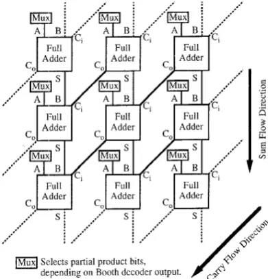
The scheme used was a Booth decoding to obtain eight partial products, which are then added in a carry-save manner as shown in the below Figure. Each full adder row receives a running sum and carry from the row above. The very top adder of each column of the summation receives one of its inputs from the accumulated total of the previous cycle, which is then fed back. Wallace tree architecture for partial product addition is not used here because such architecture would lead to larger power consumption due to large area and wiring requirements. Using the SRPL technique described above, each of the full adders in the partial product summation array is constructed.
Fig. Carry Save Addition of partial products
Performance:
margin problems that will intensify the future reduction of the supply voltage and this reduction in V, will also lead to speed degradation.
6. CONCLUSION:
A recently made high-speed, low-power logic circuit technology is proposed and it is used to implement a multiply and accumulate circuit in double metal 0.4 micron CMOS. So, In future it can be further extendable to reduce the number of transistor with low power. SRPL MAC is 0.4 ns slower than the CPL version. CPL is nearly as twice as fast as CMOS. The MAC consumes power of 34mW and it achieves a frequency of 1.50 MHz .It assures much promise for multimedia applications.
REFERENCES:
[1] A.P.Chandrakasan, and R.W.Brodersen,”low power digital CMOS design”
[2] M. Suzuki et al., “A I .5 ns 32-bit CMOS ALU in double pass-transistor logic, “in Proc.1993 IEEE Int. Solid-State Circuits Conj’,, Feb.1993, vol. 36, pp. 90-91.
[3] Low power multiplier design using delayed evaluation Gerald E. Sobelman and Donovan L. Raatz
[4] J.H.Satyanarayana and k. k parthi “A theoretical approach to estimation of bounds on power consumption in digital multipliers” [5] C.Farnsworth, D.A Edwards and S.S.Sikand, utilizing Dynamic logic for low power consumption in digital multipliers”
[6] K. Yano 3.8 ns CMOS 16 X 16 multiplier using complimentary pass-transistor logic,” IEEE J. Solid-State Circuits, vol.25. No. 2, pp. 388-395, Apr. 1990.
[7] J.M. Rabaey, M.pedram, “low power design methodologies”