IJSRSET173227 | Received : 07 March 2017 | Accepted : 23 March 2017 | March-April-2017 [(3)2: 249-253]
© 2017 IJSRSET | Volume 3 | Issue 2 | Print ISSN: 2395-1990 | Online ISSN : 2394-4099 Themed Section: Engineering and Technology
249
Pulse Width Modulation Technique Based FPGA
Implementation of Ac Motor Speed Control
1
Sundaram A,
2Kibru Mesfin Germamo,
3Bekalu Lakie Yideg
123
Department of Electrical and computer Engineering, Wolkite University, Ethiopia
ABSTRACT
In this paper a pulse width modulation is used to regulate the current sent to the motor. Unlike SCR method which switch at line frequency, PWM controls produce smoother current at higher switching frequencies, typically between 1 kHz to 20 kHz. This consists of a large reservoir capacitor and a H-bridge arrangement of switching elements e.g. thyristors, MOSFET, solid state relays or transistors. This technique is used to control the power to inertial electrical devices, made practical by modern electronic power switches. The advantage of hardware parallelism, FPGAs exceed the computing power of digital signal processors (DSPs) by breaking the paradigm of sequential execution. FPGA technology offers flexibility and rapid prototyping capabilities in the face of increased time-to-market concerns. It enables to test an idea or concept and verify it in hardware without going through the long fabrication process. The cost of making incremental changes to FPGA designs is negligible. The validity of the proposed controller is confirmed through the simulation results. To implement it in the laboratory various parameters like rotor flux, rotor current and operating points, rotor parameter tuning are to be estimated. The proposed speed control system can be useful for the variable speed drive systems.
Keywords : FPGA Implementation, PWM, SCR, AC Motor Control
I.
INTRODUCTION
In the long run of research for the speed control of AC motors, a number of control methods were implemented which replaced the application of DC drives in the upcoming industrial requirements. Solid state drives , Microprocessors, windows based Graphical User Interface (GUI), Proportional Integral Derivative (PID) controller, Fuzzy Logic Controller were the important techniques that ruled the area of speed control.
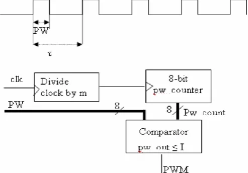
Figure 1. PWM generation and output
II.
METHODS AND MATERIAL
Figure 1 highlights the components of the physical hardware that implement the PWM. The output of this is used to control the speed of the motor. The period τ is preset as T is 40 ns for the 25 Mhz Xilinx FPGA board. The PWM is developed in verilog with only the 8-bit switches as a control input. The LEDs indicate the presence of 5V, 3V, and each bit value MSB from top. The resistors bias the LEDs and maintain a 3V input to the FPGA. Time domain appearance of the PWM, the duty cycle shown is about 25%.
of designing digital PWM Generators. The implementation of FPGA-based digital control schemes proves cost effective and hence economically suitable for small designs.
The motor should be encoder module attached so that the RPMs could be measured. In my cases the motor is attached to a 1000 pulse/rotation encoder. To measure the frequency a counter can be used. The counter is reset and is enabled for a period Tm. The counter is then incremented at the positive edge of each input signal’s pulse (SI). The count at the end of the period Tm is proportional to the speed .Tm=255* shortest period of the speed signal. Thus the measured speed will range from 0 to 255. The speed is to be measured at every sampling period. The output of the FPGA is only one BCD signal and is provided with a wire to enable each digit. The encoder output is 5V square wave that pulses 1000 times per revolution. The Speed is measured by counting for a given period that will reach a maximum of 1024 at maximum speed to obtain a higher resolution, and smooth display appearance.
Figure 2. Physical implementation of motor driver
Fig 2 shows the physical hardware of a motor driver. The largest device is the 75A POWER MOSFET, the TO-92 package is the VN0106 MOSFET, the TO-220 package is a 20L15T 20A Schottky Diode. The Electrolytic capacitor is used in parallel with the motor to for a smooth speed response of the motor.
1. PROPOSED METHOD
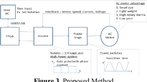
A host PC is used as an input for the AC Motor. Initially MODELSIM is used to verify and check the correct coding procedure and then the coding is written in ALTERA QUARTUS 2 software. This software is used to embed the coding into the FPGA kit. The AC motor is connected to the AC power supply through a FET. The zero crossing detector circuit observes the zero crossing of the input sine wave and generate a pulse accordingly. The output of the PWM waveform is fed as input to the FET switch. When the PWM output is high the motor is switched ON else it is OFF. This pulse is given as input to the FPGA kit. There are 3 buttons
provided on the FPGA kit for the use of reset, logic1 and logic 0. Hence the respective output waveform was obtained.
Figure 3.
Proposed Method
1.1 Design methodology
The coding for the motor speed control is written and is implemented in the MATLAB 2010a. The wave forms of the stator current, rotor speed and electromagnetic torque is obtained and are used for future reference. The same concept is used to design the required coding using MODELSIM 10.1 G and the correctness of the coding is verified. The same logic is applied in ALTERA QUADRUS II to obtain the phase controlled waves forms of various PWM pulses. This coding is given as input to the CYCLONE 3 FPGA kit and its RTL schematic is also checked to obtain the required output.
1.2 Matlab Simulink block diagram
The 230 volt ac supply is an input to the rectifier circuit, which converts ac to dc and then connected to the chopper circuit. A chopper is an electronic switch that is used to interrupt a signal under the control of the other. If the input pulse to the inverter is high then the current flows through the motor and is turned on else no current flows and is turned off.
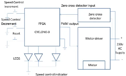
1.3 Hardware Overview
Figure 5. Hardware overview
A 230V AC supply is connected as input to the step down transformer and a desired ac output voltage is obtained that is to be converted as dc. A diode rectifier then provides a full-wave rectified voltage that is initially filtered by a simple capacitor filter to produce a dc voltage. This resulting dc voltage usually has some ripple due to the ac voltage variation. The regulator circuit maintains a constant dc voltage even for any variation in the input dc voltage or any variation in the output dc voltage due to the change in load. This voltage regulation is obtained using the popular voltage regulator IC units.
Figure 5 shows the waveform at different level across the zero crossing detector circuit. The first waveform is the output of the (0-12V) transformer, the second is the output of the bridge rectifier (12V pulsating DC) and the third is the output of the Zero crossing detector. The NPN transistor is turned on for an input voltage above 0.5V and is off less than that. Under off condition the output voltage is Zero, which is detected by the device.
1.4. AC motor driver circuit and design
To access the AC control circuit through PC, the desiged AC circuit is to be connected with the PC. The interfacing diagram for AC control circuit with test motor is shown in the figure 6.
Figure 6. Interfacing ac circuit with motor
In the process of interfacing the zero crossing detectors is connected to the first pin of the parallel port. A program is developed to control the input voltage of the COC test bench. This program is developed to create a delay sinal, varying from 0ms to 10 ms at regular intervals and at the every interval the pulse [5V logic 0.5 ms duration] is set to the parallel port pin no2 to control the AC control circuit. The MOC 3021 is used to isolate the high power from the PC and more over 40 mA is enough to drive the photo detector based TRIAC driver MOC 3021.The output of the MOC 3021 is able to drive the TRIAC. The time delay is adjusted in the program between 0ms to 10ms to obtain a variable voltage from 0 to 230V. To turn off the transistor the input logic1 is given to the pin 2 and the collector current is reduced to 0mA which is not enough to drive the photo detector based TRIAC driver MOC 3021. The output of this MOC 3021 is not able to drive the TRIAC. So there is no any conduction portion in the input wave from.
III. RESULTS AND DISCUSSION
A.
MATLAB simulation output for proposed
method
In figure 7, the various characteristics of AC Motor such as the stator current, rotor speed and electromagnetic torque is obtained as shown using MATLAB 10.2V. It is seen that a smooth transition of Rotor speed and constant speed value were obtained at 500A.
B.
PWM output waveform 1:
Whenever the output Sine waveform passes through the Zero Crossing detector, a pulse is generated. This pulse is given as input to the FPGA kit. There are 3 buttons assigned on the FPGA kit for the purpose of reset, logic1 and logic 0. The wave form is obtained as shown below. This also indicates the ON time duration of both the pulses and it is seen that the duration of ON time of first pulse is greater than that of the second pulse.
Figure 8. PWM output waveform 1
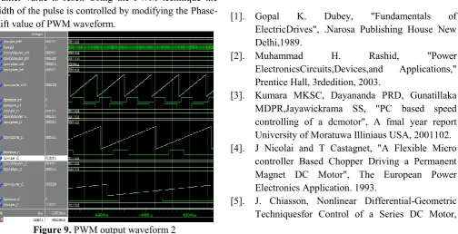
C. PWM output waveform 2
The input is similar to PWM technique but an addition Counter is also used. A pulse is produced whenever the counter value is reset. Using the PWM technique the width of the pulse is controlled by modifying the Phase-shift value of PWM waveform.
Figure 9. PWM output waveform 2
The RTL view of proposed system is shown in Fig 10. The main components are Frequency divider circuit, PWM pulse generator and Duty cycle variation component. The input is given to the FPGA kit via Zero crossing detector and the output is obtained at the PWM pulse generator
Figure 10. RTL view of proposed system
IV. CONCLUSION
The AC motor speed control has been implemented using FPGA in VLSI technology making the program reconfigurable. The main drawback of the earlier method has been overcome and a PWM wave with required phase control is obtained for controlling the speed of the AC motor. By this proposed method a smoother sine wave is obtained, rather than the stepped sine wave obtained from the other methods which are the most important factor for efficiently controlling the motor speed. The main advantages of AC motor speed control by this method includes fast learning capability, robust control rules and improved performance with FPGA.
V.
REFERENCES
[1]. Gopal K. Dubey, "Fundamentals of
ElectricDrives", .Narosa Publishing House New Delhi,1989.
[2]. Muhammad H. Rashid, "Power
ElectronicsCircuits,Devices,and Applications," Prentice Hall, 3rdedition, 2003.
[3]. Kumara MKSC, Dayananda PRD, Gunatillaka MDPR,Jayawickrama SS, "PC based speed controlling of a dcmotor", A fmal year report University of Moratuwa Illiniaus USA, 2001102. [4]. J Nicolai and T Castagnet, "A Flexible Micro
controller Based Chopper Driving a Permanent Magnet DC Motor", The European Power Electronics Application. 1993.
IEEE Transactionson Control Systems Technology.vol 2, p. 35-42,1994.
[6]. A Khoei Kh.Hadidi, "MicroProcessor Based Closed- Loop Speed Control System for DC Motor Using Power MOSFET", 3rd IEEE international conference on Electronics, Circuits and Systems( 1996) vol.2, pp.1247-1250.
[7]. Peter Spasov, "Microcontroller Technology: The 68HC11" Prentice Hall, 5th edition, 2004. 8In System Programming (ISP) for ATMEL chips, http://www.ikalogic.com/isp.php.
[8]. Pulse width modulator module (PWMM),
ATmega8L data sheet.
[9]. ADC devices, ATmega8L data sheet.
[10]. LCD interfacing, the microcontroller and
embedded systems by Muhammad Ali
Mazidi,Janice GillispieMazidi, Rolin D.