IJEDR1702122
International Journal of Engineering Development and Research (www.ijedr.org)723
SIMULATION AND IMPLEMENTATION OF MULTILEVEL
INVERTER BASED INDUCTION MOTOR DRIVE BASED ON
PWM TECHNIQUES
1
CH.Manasa,
2K.Uma,
3D.Bhavana
Students of B.Tech, Electrical and Electronics Depart ment BRECW, JNTUH, Te langana. Under the guidance of Racharla Manju Bhargavi, Associate Professor, Depart ment of
EEE,BRECW,JNTUH,India,man ju.racharla@g mail.co m
Abstract — The main objective of this paper is to control the speed of an induction motor by using five level diode clamped mu ltilevel inverter. To obtain high quality sinusoidal output voltage with redu ced harmonics, mult icarrier PWM control scheme is proposed for diode clamped multilevel inverter. An open loop speed control can be achieved by using V/ƒ method. This method can be imple mented by change the supply voltage and frequency applied to the three phase induction motor at constant ratio. The proposed system is an effective replace ment for the conventional method which produces high switching losses, res ults in poor drive performance. The simulat ion results reveal that the proposed circuit effectively controls the motor speed and enhances the drive performance through reduction in total harmonic d istortion (THD).
Keywords — Diode clamped mu ltilevel inverter, Induction motor, Mu lticarrier PWM technique, THD, V/ƒ method.
I. INTRODUCTION
Majority of industrial drives use ac induction motor because these motors are rugged, reliable, and relat ively ine xpensive. Induction motors are mainly used for constant speed applications because of unavailability of the variable -frequency supply voltage. But many applications need variable speed operations. Historica lly, mechanica l gear systems were used to obtain varia ble speed. Recently, power e lectronics and control systems have matured to allo w these components to be used for motor control in place of mechanical gears. These electronics not only control the motor’s speed, but can improve the motor’s dynamic and steady state characteristics. Adjustable speed ac machine system is equipped with an ad justable frequency drive that is a power e lectro nic device for speed control of an electric mach ine. It con trols the speed of the electric machine by converting the fixed voltage and frequency to adjustable values on the machine side.
High power induction motor drives using classical three phase converters have the disadvantages of poor voltage and current qualities. To improve these values, the switching frequency has to be raised which causes additional switching losses. Another possibility is to put a motor input filter between the converter and motor, wh ich causes additional weight. A further inconvenience is the limited voltage that can be applied to the induction motor determined by inconvenience is the limited voltage that can be applied to the induction motor determined by the blocking voltage of the semiconductor switches. The concept of mu ltile vel inverter control has opened a new possibility that induction motors can be controlled to achieve dynamic performance equally as that of dc motors . Recently many schemes have been developed to achieve mult ilevel vo ltage profile , particula rly suitable for induction motor drive applications. The diode clamp method can be applied to higher level converters. As the number of le vel increases, the synthesized output waveform adds more steps, producing a staircase waveform. A zero harmon ic distortion of the output wave can be obtained by an infinite nu mber of levels . Unfortunately, the number of the achievable levels is quite limited not only due to voltage unbalance problems but also due to voltage clamp ing require ment, circuit layout and packaging constraints.
In this paper, a three-phase diode clamped mult ileve l inverter fed induction motor is described. The diode clamped inve rter provides multiple voltage levels fro m a series bank of capacitors. The voltage across the switches has only half of the dc bus voltage. These features effectively double the power rating of voltage source inverter for a given semiconductor device. The proposed inverter can reduce the harmonic contents by using multica rrier PWM technique. It generates motor currents of high quality. V/ƒ is an efficient method for speed control in open loop.
In this scheme, the speed of induction machine is controlled by the adjustable magnitu de of stator voltages and its frequency in such a way that the air gap flu x is always maintained at the desired value at the steady-state. Here the speed of an induction motor is precisely controlled by using three level d iode cla mped mu ltilevel inverter.
II. CONVENTIONAL MET HOD
The voltage source inverter produces an output voltage or a current levels can be zero or ±Vdc/2 or ±Vdc. This is known as three level inverter. To obtain the quality output voltage or a current waveform with a min imu m a mount of ripple content, it requires high switching frequency along with various pulse width modulation strategies. In high- power and high voltage applications, these three-level inverters have some limitations in operating at high frequency main ly due to switching losses and constraints of device ratings. The dc link voltage of a three-level Inverter is limited by voltage ratings of switching devices; the problemat ic series connection of switching devices is required to raise the dc link vo ltage.
IJEDR1702122
International Journal of Engineering Development and Research (www.ijedr.org)724
Figure 1: Three le vel Inver terFro m the aspect of harmonic reduction and high dc link voltage level, three-level approach seems to be the most promising alternative. The harmonic contents of a three-level inverter are less than that of a two-level inverter at the same switching frequency and the blocking voltage of the switching device is half of the dc -link vo ltage. A three level inverter will not generate common-mode voltages when the inverter output voltages are limited within certain of the available switching states. So the three level inverter topology is generally used in rea lizing the high performance, h igh voltage ac drive systems.
III. DRIVE S YS YEM DES CRIPTION
In the conventional technique normal PWM method is used. So that the voltage and current is of poor qualities and the switching frequency causes more a mount of switching losses. Those drawbacks are rectified using three phase diode clamped mu ltilevel inverter.
Structure of five Level Diode Cla mped Mult ilevel Inverter :
Fig.2. Multile vel inverter based dri ve circuit
IJEDR1702122
International Journal of Engineering Development and Research (www.ijedr.org)725
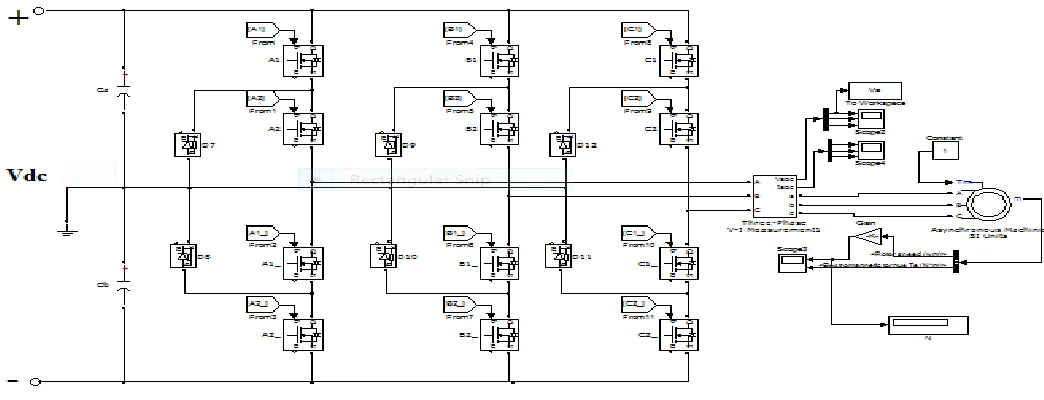
Single leg Diagram of Fi ve le vel inverterThe five-level neutral point-cla mped voltage source inverter is shown in Fig.2.It contains 24 unidirect ional active switches and 18 neutral point clamp ing diodes. The middle point of the four capacitors ―n” can be defined as the neutral point. The major benefit of this configuration is each switch must block only one-fourth of the dc link voltage (Vdc/4). In order to produce fiv e levels, only four of the eight switches in each phase leg should be turned on at any time. The d c-bus voltage is split into five le vels by four series-connected bulk capacitors, C1, C2, C3 and C4 they are same in rating.For DC bus voltage Vdc, the voltage across each capacitor is Vdc/4 and each device voltage stress will be limited to one capacitor voltag e levels Vdc/4 through clamp ing diodes. The diodes are all same type to provide equal voltage sharing and to clamp the same voltage level across the switch, when the switch is in off condition. Hence this structure provides less voltage stress across the s witch.
IV. PRINCIPLE OF OPERATION
To p roduce a staircase-output voltage, consider one leg of the three-leve l inverter, as shown in Fig.3. The steps to synthesize the three-level voltages are as follows.
a. For voltage levels Van = Vdc/ 2 turn on all upper switches S1-S4.
b. For voltage level Van= Vdc/ 4, turn on three upper switches S2-S4 and lowe r switch S5.
c. For voltage level Van=0, turn on two upper switches S3 and S4 and two lower switches S5 and S6. d. For voltage levels Van = -Vdc/4, turn on one upper switch S4 and three lo wer switches S5-S7. e. For voltage levels Van = -Vdc/2, turn on all lower switches S5-S8.
NPC inverter which has been extensively used today in industrial drives, traction as well as FACT’s system Based on concept o f using diodes to limit power devices voltage stress Output phase voltage can assume any voltage level by selecting any of the nodes.
Table.1. shows the voltage levels and their corresponding switch states. State condition 1 means the switch is on, 0 means th e switch is off. There are two co mple mentary switch pairs in each phase.
These pairs for one leg of the inverter are (S1, S5), (S2, S6), (S3, S7), (S4, S8). If one of the comp le mentary switch pa irs is turned on, the other of the same pair must be off.
TABLE 1
IJEDR1702122
International Journal of Engineering Development and Research (www.ijedr.org)726
Fig.4. shows the phase voltage waveform of the three-level inverter. The m-level converter has an m-leve l output phase-leg voltage and a (2m-1)-level output line voltage.Fig.4. Three le vel inve rter output voltage.
The most attractive features of multilevel inverters are as fo llo ws.
a. They can generate output voltages with e xtre me ly low d istortion and lower dv/dt. b. They draw input current with very lo w distortion.
c. They generate smalle r co mmon- mode (CM) voltage, thus reducing the stress in the motor bearings. d. They can operate with a lowe r switching frequency.
V. PROPOS ED SCHEME
The bloc k schematic of mu ltilevel inverter fed three phase induction motor is as shown in Fig.5. The comp lete system will consist of two sections; a power circuit and a control circuit. The power section consists of a power rectifie r, filter capacitor, and three phase diode clamped mu ltilevel inverter. The motor is connected to the multilevel inverter. An ac input voltage is fed to a three phase diode bridge rectifier, in order to produce dc output voltage across a capacitor filter. A capacitor filte r, re moves the ripple contents present in the dc output voltage. The pure dc voltage is applied to the three phase multilevel inverter through capacitor filter. The mu ltilevel inverter has 24 IGBT switches that are controlled in order to generate an ac output voltage from the dc input voltage. The control circuit of the proposed system ma in ly consists of gate driver circuit. Here Mult icarrier PWM technique is used for the production of gate pulses to the IGBT switches. The output ac voltage is obtained from the mu ltile vel inverter can be controlled in both magnitude and frequency (V/ ƒ open loop control). The controlled ac output voltage is fed to the induction motor drive. When the power switches are on, current flows from the dc bus to the motor winding. The motor wind ings are highly inductive in nature; they hold electric energy in the form of current. This current needs to be dissipated while switches are off. Diodes are connected across the switches give a path for the current to dissipate when the switches are off. These diodes are also called freewheeling diodes. The V/ƒ control method permits the user to control the speed of an induction motor at diffe rent rates. For continuously variable speed operation, the output frequency of multilevel inverter must be varied. The applied voltage to the motor must also be varied in linear proportion to the supply frequency to ma intain constant motor flu x.
Fig.5. B asic bl ock diagram
VI. MODULATION STRATEGY
Th is Paper ma inly focuses on multicarrier PWM method. This method is simple and mo re fle xib le than SVM methods. The mu lticarrier PWM method uses several triangular carrier signals, keeping only one modulating sinusoidal signal. If an n -le vel inverter is employed, n-1 carrie rs will be needed. The carriers have the same frequency WC and the same peak to peak amplit ude Ac and are disposed so that the bands they occupy are contiguous. The zero refe rence is placed in the middle of the carrie r s et. The modulating signal is a sinusoidal signal of frequency Wm and amplitude Am. At every instant each carrier is compared with the modulating signal. Each comparison gives 1(-1) and 2(-2), if the modulating signal is greater than the triangular carrier sig nal then the pulse is produced. The results are added to give the voltage level, wh ich is required at the output terminal of the inverte r. Multicarrier PWM method can be categorized into two groups:
1) Ca rrier Disposition (CD) method 2) Phase shifted PWM method. Advantages of mu lticarrie r PWM techniques:
a. Easily e xtensible to high nu mber of levels. b. Easy to imple ment.
IJEDR1702122
International Journal of Engineering Development and Research (www.ijedr.org)727
Re lated to the way the carrier waves are placed in re lation to the reference signal, three cases can be distinguished: Alternative Phase Opposition Disposition (APOD), where each carrie r band is shifted by 180° fro m the adjacent bands. Phase Opposition Disposition (POD), where the carriers above the zero reference are in phase, but shifted by 180° fro m
those carriers below the ze ro refe rence.
In-Phase Disposition (PD), where a ll the carrie rs are in phase. In this paper the gating pulses for MOSFET switches are generated by using In-phase disposition technique.
In this paper the gating pulses for IGBT switches are generated by using In-phase disposition technique.
Fig.6. In-phase disposition techni que
VII. V/ƒ CONTROL THEORY
Fig.7. shows the relation between the voltage and torque versus frequency. The voltage and frequency being increased up to the base speed. At base speed, the voltage and frequency reach the rated values. We can drive the motor beyond base speed by increasing the frequency further. But the voltage applied cannot be increased beyond the rated voltage.
The refore, only the frequency can be increased, which results in the field weaken ing and the torque available being reduced. Above base speed, the factors governing torque become co mple x, since friction and wind age losses increase significantly at higher speeds.
Hence, the torque curve becomes nonlinear with respect to speed or frequency.
Fig.7. S pee d-Tor que c har acteristics with V/ƒ contr ol
VIII. SIMULATED CIRCUITS AND WAVEFORMS
IJEDR1702122
International Journal of Engineering Development and Research (www.ijedr.org)728
Fig.8. PWM simulation circuitFig.9. shows the waveform of sine-triangle intersection. Two carrie rs together with modulation signal have been used to obtain SPWM control.
IJEDR1702122
International Journal of Engineering Development and Research (www.ijedr.org)729
Simu lated model for entire circuit is shown in Fig.10Fig.10. Simulate d circuit
Output voltage waveforms for 50 Hz frequency are s hown in below figure 11
Fig.11. Output line-line voltage for 50 Hz fre quency
IJEDR1702122
International Journal of Engineering Development and Research (www.ijedr.org)730
Fig.12. FFT for output voltageSpeed-Torque curves for 50 Hz and 45 Hz frequencies are shown in figures 13 and 14.
Fig.13. N-T c ur ves for 50 Hz fre quenc y
IJEDR1702122
International Journal of Engineering Development and Research (www.ijedr.org)731
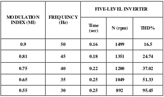
The speed-torque curves conclude that the voltage and frequency applied to the motor gets decreased; then the speed of an induction motor a lso decreased simultaneously.TABLE 2: Speed range for different MI and frequency values.
MO DULATIO N INDEX (MI)
FREQ UENC Y (Hz)
FIVE-LEV EL INV ERTER
Time
(sec) N (rpm) THD%
0.9 50 0.16 1499 16.5
0.81 45 0.18 1351 24.74
0.75 40 0.22 1200 37.02
0.65 35 0.25 1049 51.33
0.55 30 0.25 892 95.45
CONCLUS ION
In this paper a d iode cla mped mu ltilevel inverter has been presented for drive applications. The mult icarrier PWM technique can be imp le mented for producing low harmonic contents in the output, hence the high quality output voltage was obtained. The open loop speed control was achieved by maintain ing V/ƒ ratio at constant value. The simulat ion results show that the proposed system effectively controls the motor speed and enhances the drive performance through reduction in total harmonic distortion (THD). This drive system can be used for variable speed applications like conveyors, rolling mills, printing machines, Blo wers and fans, Text ile machinery and Crushers, Electric vehicle drives etc.
REFERENCE
[1] Jose, Steffen Sernet, Bin Wu, Jorge and Samir Kouro, ―Multileve l Voltage – Source - Converter Topologies for Industrial Med iu m Vo ltage Drives,‖ IEEE Trans on Industrial Electronics, vol.54, no.6, Dec 2007.
[2] Dr.Rama Reddy and G.Pandian, ―Implementation of Multilevel inverter fed Induction motor Drive,‖ Journal of Industrial Technology, vol 24, no. 1, April 2008.
[3] Nikolaus P. Schibli, T. Nguyen, and Alfred C. Rufer, ―AThree- Phase Multilevel Converter for High - Power Induction Motors,‖ IEEE Trans on Power Electronics,vol.13, no.5, Sept 1998.
[4] N.Celanovic and D.Boroyevich, ― A Comprehensive study of neutral-point voltage balancing problem in three level neutral - point- clamped voltage source PWM inverters,‖IEEE Trans on Power Electronics, vol.15, no. 2, pp. 242 – 249, March 2000. pp. 1098-1107, Sept.1999. 5.Leon M.Tolbert, Fang Zheng Peng and Thomas G.Habetler, ―Multileve l PWM methods at Low modulat ion Indices,‖ IEEE Trans on Power Electronics,vol.15, no.4, July 2000.
[5] N.S. Choi, J.G.Cho, and G.H.Cho, ―A general Circu it topology of multilevel inverter,‖ in Proc. IEEE PESC’91, 1991, pp.96-103.