Freescale Semiconductor
Document Number: AN3895
Application Note
Rev. 2, 02/2013
MPR121 Serial Communication
INTRODUCTIONThe MPR121 uses an I2C Serial Interface. The I2C protocol implementation and the specifics of communicating with the Touch Sensor Controller are detailed in this application note.
SERIAL-ADDRESSING
The MPR121 operates as a slave that sends and receives data through an I2C two-wire interface. The interface uses a Serial Data Line (SDA) and a Serial Clock Line (SCL) to achieve bidirectional communication between master(s) and slave(s). A master (typically a microcontroller) initiates all data transfers to and from the MPR121, and it generates the SCL clock that synchronizes the data transfer.
The MPR121 SDA line operates as both an input and an open-drain output. A pullup resistor, typically 4.7 kΩ, is required on SDA. The MPR121 SCL line operates only as an input. A pullup resistor, typically 4.7 kΩ, is required on SCL if there are multiple masters on the two-wire interface, or if the master in a single-master system has an open-drain SCL output.
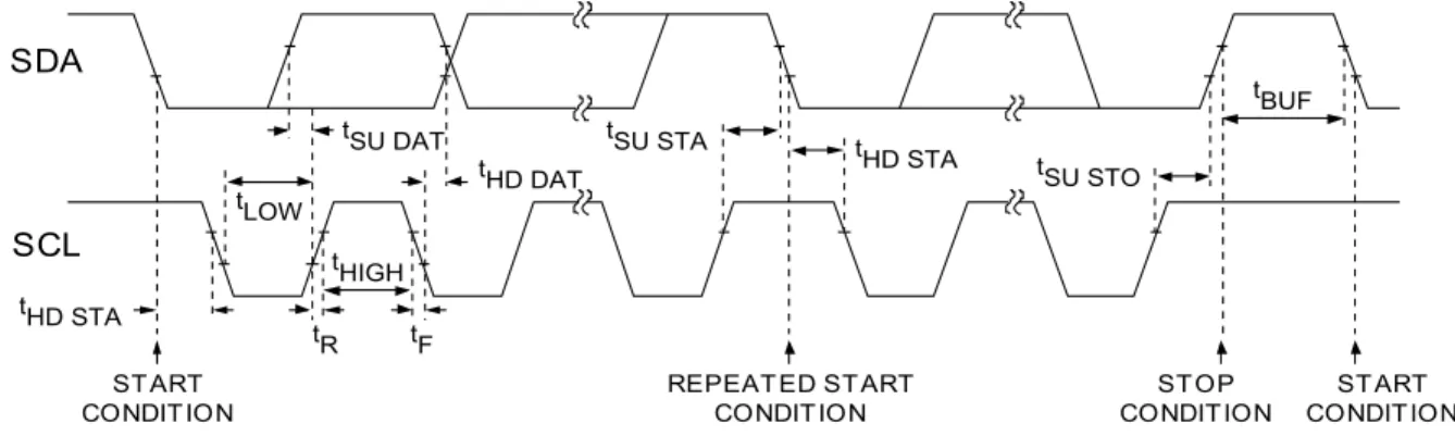
Each transmission consists of a START condition (Figure 1) sent by a master, followed by the MPR121’s 7-bit slave address plus R/W bit, a register address byte, one or more data bytes, and finally a STOP condition.
Figure 1. Wire Serial Interface Timing Details
SCL
SDA
tLOW tHIGH
tF tR tHD STA
tHD DAT tHD STA
tSU DAT tSU STA tBUF
tSU STO
START CONDITION STOP
CONDITION REPEATED START
CONDITION START
MPR121 Serial Communication, Rev. 2
2 Freescale Semiconductor, Inc.
START AND STOP CONDITIONS
Both SCL and SDA remain high when the interface is not busy. A master signals the beginning of a transmission with a START (S) condition by transitioning SDA from high to low while SCL is high. When the master has finished communicating with the slave, it issues a STOP (P) condition by transitioning SDA from low to high while SCL is high. The bus is then free for another transmission.
Figure 2. Start and Stop Conditions BIT TRANSFER
One data bit is transferred during each clock pulse (Figure 3). The data on SDA must remain stable while SCL is high.
Figure 3. Bit Transfer ACKNOWLEDGE
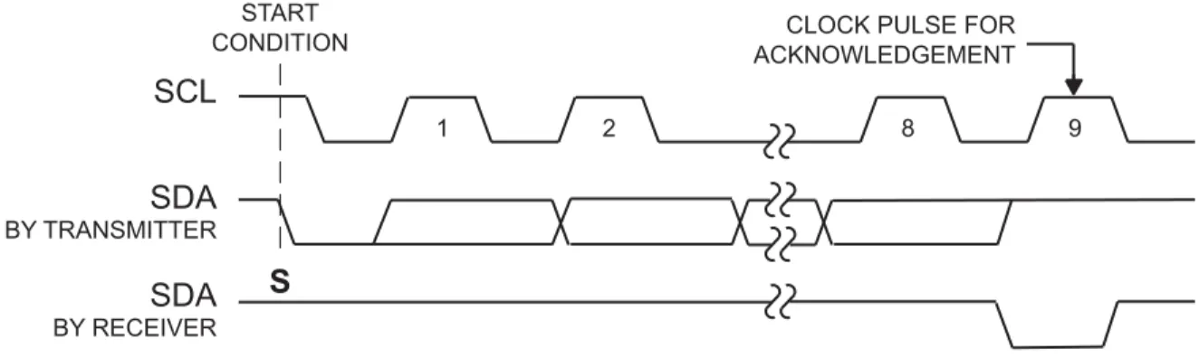
The acknowledge bit is a clocked 9th bit (Figure 4) which the recipient uses to handshake receipt of each byte of data. Thus each byte transferred effectively requires nine bits. The master generates the 9th clock pulse, and the recipient pulls down SDA during the acknowledge clock pulse, such that the SDA line is stable low during the high period of the clock pulse. When the master is transmitting to the MPR121, the MPR121 generates the acknowledge bit, since the MPR121 is the recipient. When the MPR121 is transmitting to the master, the master generates the acknowledge bit, since the master is the recipient.
Figure 4. Acknowledge
DATA LINE STABLE
DATA VALID CHANGE OF
DATA ALLOWED
SDA
SCL
START CONDITION
SDA
SCL
STOP CONDITION
P
S
START CONDITION
SDA
BY TRANSMITTER
S
1 2 8 9
CLOCK PULSE FOR ACKNOWLEDGEMENT
SDA
BY RECEIVER
SLAVE ADDRESS
The MPR121 has selectable slave addresses listed by different ADDR pin connections. This also makes it possible for multiple MPR121 devices to be used together for channel expansions in a single system.
MESSAGE FORMAT FOR WRITING THE MPR121
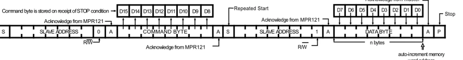
A write to the MPR121 comprises the transmission of the MPR121’s keyscan slave address with the R/W bit set to 0, followed by at least one byte of information. The first byte of information is the command byte. The command byte determines which register of the MPR121 is to be written by the next byte, if received. If a STOP condition is detected after the command byte is received, the MPR121 takes no further action (Figure 5) beyond storing the command byte. Any bytes received after the command byte are data bytes.
Figure 5. CommandByte Received
Any bytes received after the command byte are data bytes. The first data byte goes into the internal register of the MPR121 selected by the command byte (Figure 6).
Figure 6. Commandand Single Data Byte Received
If multiple data bytes are transmitted before a STOP condition is detected, these bytes are generally stored in subsequent MPR121 internal registers because the command byte address generally auto-increments.
Table 1. MPR121 Slave Address ADDR Pin Connection I2C Address
VSS 0x5A
VDD 0x5B
SDA 0x5C
SCL 0x5D
S
SLAVE ADDRESS0
A
COMMAND BYTEA
P
Acknowledge from MPR121
R/W
Acknowledge from MPR121 D15 D14 D13 D12 D11 D10 D9 D8 Command byte is stored on receipt ofSTOP condition
S SLAVE ADDRESS 0 A COMMAND BYTE A DATA BYTE A P
Acknowledge from MPR121
R/W 1 byte
Auto-increment memory word address D15 D14 D13 D12 D11 D10 D9 D8 D7 D6 D5 D4 D3 D2 D1 D0 Howcommand byte and data byte
map into MPR121's registers
Acknowledge from
MPR121 Serial Communication, Rev. 2
4 Freescale Semiconductor, Inc.
MESSAGE FORMAT FOR READING THE MPR121
MPR121 is read using MPR121's internally stored register address as address pointer, the same way the stored register address is used as address pointer for a write. The pointer generally auto-increments after each data byte is read using the same rules as for a write. Thus, a read is initiated by first configuring MPR121's register address by performing a write (Figure 5)followed by a repeated start. The master can now read 'n' consecutive bytes from MPR121, with first data byte being read from the register addressed by the initialized register address.
Figure 7. Reading MPR121 OPERATION WITH MULTIPLE MASTER
The application should use repeated starts to address the MPR121 to avoid bus confusion between I2C masters.On a I2C bus, once a master issues a start/repeated start condition, that master owns the bus until a stop condition occurs. If a master that does not own the bus attempts to take control of that bus, then improper addressing may occur. An address may always be rewritten to fix this problem. Follow I2C protocol for multiple master configurations.
S SLAVE ADDRESS 1 A DATA BYTE A P R/W n bytes
auto-increment memory word address D1 D0 D3 D2 D5 D4 D7 D6 Acknowledge from MPR121
Acknowledge from master
S 0 A A
Acknowledge from MPR121 R/W
Acknowledge from MPR121 D15 D14 D13 D12 D11 D10 D9 D8 Command byte is stored on receipt ofSTOP condition
SLAVE ADDRESS COMMAND BYTE
Repeated Start
Document Number: AN3895 Rev. 2
Information in this document is provided solely to enable system and software implementers to use Freescale products. There are no express or implied copyright licenses granted hereunder to design or fabricate any integrated circuits based on the information in this document.
Freescale reserves the right to make changes without further notice to any products herein. Freescale makes no warranty, representation, or guarantee regarding the suitability of its products for any particular purpose, nor does Freescale assume any liability arising out of the application or use of any product or circuit, and specifically disclaims any and all liability, including without limitation consequential or incidental damages. “Typical” parameters that may be provided in Freescale data sheets and/or specifications can and do vary in different applications, and actual performance may vary over time. All operating parameters, including “typicals,” must be validated for each customer application by customer’s technical experts. Freescale does not convey any license under its patent rights nor the rights of others. Freescale sells products pursuant to standard terms and conditions of sale, which can be found at the following address: freescale.com/salestermsandconditions.
How to Reach Us:
Home Page:
freescale.com
Web Support:
freescale.com/support
Freescale, the Freescale logo, AltiVec, C-5, CodeTest, CodeWarrior, ColdFire, C-Ware, Energy Efficient Solutions logo, Kinetis, mobileGT, PowerQUICC, Processor Expert, QorIQ, Qorivva, StarCore, Symphony, and VortiQa are trademarks of Freescale Semiconductor, Inc., Reg. U.S. Pat. & Tm. Off. Airfast, BeeKit, BeeStack, ColdFire+, CoreNet, Flexis, MagniV, MXC, Platform in a Package, QorIQ Qonverge, QUICC Engine, Ready Play, SafeAssure, SMARTMOS, TurboLink, Vybrid, and Xtrinsic are trademarks of Freescale Semiconductor, Inc. All other product or service names are the property of their respective owners.