462
All Rights Reserved © 2013 IJARCSEE Abstract—
metastability is becoming a serious problem in high-performance VLSI design, mainly due to the relatively-high probability of error when a bistable circuit operates at high frequencies. dynamic latchesare widely used in high-performance VLSI circuits, mainly dueto their lower cost and higher operation speed than static latches. In this work, we demonstrate that dynamic memory cells presentan anomalous behavior referred to as metastable operation with characteristics similar to those of static latches. During every cycle, the relative time of the two signals changes a bit, and eventually they switch sufficiently close to each other, leading to metastability. With multiple clock domains on the same chip, synchronizers are required when on-chip data crosses the clock domain boundaries. Any flip-flop can easily be made metastable. Toggle its data input simultaneously with the sampling edge of the clock, and you get metastability. One common way to demonstrate metastability is to supply two clocks that differ very slightly in frequency to the data and clock inputs.
I.INTRODUCTION
Metastability in digital systems occurs when two asynchronous signals combine in such a way that their resulting output goes to an indeterminate state. A common example is the case of data violating the setup and hold specifications of a latch or a flip-flop. In a synchronous system, the data always has a fixed relationship with respect to the clock. When that relationship obeys the setup and hold requirements for the device, the output goes to a valid state within its specified propagation delay time. However, in an asynchronous system, the relationship between data and clock is not fixed; therefore, occasional violations of setup and hold times can occur. When this happens, the output may go to an intermediate level between its two valid states and remain there for an indefinite amount of time before resolving itself or it may simply be delayed before making a normal transition. In either case, a metastable event has occurred.[1]
Metastable events can occur in a system without causing a problem, so it is necessary to define what constitutes a failure before attempting to calculate a failure rate. For a simple CMOS latch, as shown in Figure 1, valid data must be present on the input for a specified period of time before the clock signal arrives (setup time) and must remain valid for a specified period of time after the clock transition (hold time) to assure that the output functions predictably. This leaves a small window of time with respect to the clock (t0 ) during
which the data is not allowed to change. If a data edge occurs within this aperture, the output may go to an intermediate level and remain there for an indefinite amount of time before resolving itself either high or low, as illustrated in Figure 2. This metastable event can cause a failure only if the output has not resolved itself by the time that it must be valid for use (for example, as an input to another stage); therefore, the amount of resolve time allowed a device plays a large role in calculating its failure rate.
II.FAILURE MODES
metastability is an inevitable result of any attempt to map a continuous domain to a discrete one. There will always be points in the continuous domain which are equidistant (or nearly so) from the points of the discrete domain, making a decision as to which discrete point to select a difficult and potentially lengthy process. If the inputs to an arbiter or flip-flop arrive almost simultaneously, the circuit most likely will traverse a point of metastability. Metastability remains poorly understood in some circles, and various engineers have proposed their own circuits said to solve or filter out the metastability; typically these circuits simply shift the occurrence of metastability from one place to another.Chips using multiple clock sources are often tested with tester clocks that have fixed phase relationships, not the independent clocks drifting past each other that will be experienced during operation. This usually explicitly prevents the metastable failure mode that will occur in the field from being seen or reported.
III. The Synchronization Problem
While there have been many promising asynchronous design examples, asynchronous design is still not seeing widespread use. One important reason for this is that
METASTABILITY ERRORS IN CMOS INTERFACE
CIRCUITS
Sachin Bandewar1, Mala Kushwaha,2 Shweta Raghuwanshi3
Asynchronous designs must communicate with other parts of the system which typically operate synchronously. Unfortunately, this is difficult to do reliably without substantial latency penalties. When this latency penalty is taken into account, most, if not all, of the performance advantage gained by an asynchronous design is lost. Even if no asynchronous modules are used, synchronous modules operating at different clock rates or out of phase can have the same problem.[3]
The latter problem is becoming more significant as it becomes increasingly difficult to distribute a single global clock to all parts of the chip. Many designers today are considering the necessity of having multiple clock domains on a single chip, and they will need to face this problem. A synchronization problem can occur when a synchronous circuit must synchronize an asynchronous input. This can be done using a single D-type flip-flop as shown in Figure 1(a). However, if the clock edge arrives too close in time to data arriving from an asynchronous circuit, the circuit may enter a metastable state in which its output is at neither a logic 0 or logic 1 level, but rather, lies somewhere in between. This behavior is depicted in Figure 1(b). Assume that Q is initially low and that D has recently gone high. If D goes low again at about the same time that CLK rises, the output Q may start to rise and then get stuck between the logic levels as it observes D falling. Should Q rise or fall? Actually, either answer would be okay, but the flip-flop becomes indecisive. At some point, Q may continue to a logic 1 level, or it may drop to the logic 0 level. [2]
Fig. 1. (a) Simple, dangerous synchronizer. (b) Oscilloscope view of metastable behavior.
He goes on to discuss how the designers of the ENIAC used additional flip-flops to allow more time to synchronize asynchronous inputs. This paper states that this technique does not eliminate the chance of error, but rather, it simply
reduces its probability. This paper also presents a method of determining the probability of error. The problem appears to be largely ignored until 1966 when Catt rediscovered it and presents a different formulation of this error probability. Again, it appears that the synchronization problem was not widely known or understood. Evidence of this is that several asynchronous arbiters designed in the early 1970s suffered from metastability problems if arrival times of signals are not carefully controlled. Finally, in 1973 experimental evidence of the synchronization problem presented by Chaney and Molnar appears to have awakened the community to the problem. After this paper, a number of papers were pub- lished that provided experimental evidence of metastability due to asynchronous inputs, and mathematical models were developed to explain the experimental results. Pechoucek’s paper also shows that the only way to reduce the probability to zero is to generate the clock locally and be able to stop the clock when metastability occurs. Over the years, there have also been several proofs that show
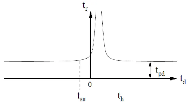
Fig. 2. Flip-flop response time as function of input arrival
time in relation to clock arrival time (clock arrives at 0). that metastability in a bistable is unavoidable and that it is related to other issues such as arbitration and hazards .
IV. Probability of Synchronization Failure
464
All Rights Reserved © 2013 IJARCSEE
distributed within the clock cycle. Therefore, the probability that the data arrives at a time td which falls between tsu and th is given below.
where T is the length of the clock period. If we assume that the flip-flop is given some bounded amount of time, tb, to decide whether or not to accept the newly arrived data, the probability of a synchronization failure is related to the probability that the response time, tr, exceeds tb. In the metastable region between tsu and th, it can be shown that the response time increases in an approximately exponential fashion. Therefore, if td falls in this range, the probability that tr > tb can be expressed as follows:
where k and _ are circuit parameters, with k being a positive fraction less than 1 and _ being a time constant with values on the order of a few picoseconds for modern technologies. Combining Equations 1 and 2 using Bayes rule, we get:-
If tb − tpd _ 5_, Equation 3 can be simplified as follows:
By combining constants, Equation 5 can be changed to
Equation 6 is convenient since there is only two circuit-dependent parameters T0 and _ that need to be determined experimentally. These parameters appear to scale linearly with feature size. Equation 6 has been verified experimentally and found to be a good estimate as long as tb is not too close to tpd. It is important to note that there is no finite value of tb such that P(tr > tb) = 0. Therefore, the response time in the worst-case is unbounded.
A synchronization error occurs when tr is greater than the time available to respond, ta. A synchronization failure occurs when there is an inconsistency caused by the error. Failures occur less often than errors since a consistent interpretation still may be made even when there is an error. The expected number of errors is
where _ is the average rate of change of the signal being sampled and t is the time over which the errors are counted. If we assume all errors are failures, set Ee(ta) to 1, change t to
MTBF (mean time between failure), substitute Equation 6 for P(tr > ta), and rearrange Equation 7, we get
This equation increases rapidly as ta is increased. Therefore, even though there is no absolute bound in which no failure can ever occur, there does exist an engineering bound in which there is an acceptably low likelihood of error. [4]
V. Reducing the Probability of Failure
Many techniques have been devised to address the metastability problem and reduce the probability of synchronization failure to an acceptable level when interfacing between synchronous and asynchronous mod- ules. The goal of each of these techniques is to increase the amount of time to resolve the metastability (i.e., increase ta). The simplest approach to achieve this is to use two (or more) latches in series as shown in Figure 3 to sample asynchronous signals arriving at a synchronous module. This increases the time allowed for a metastable condition to resolve. In other words, if n extra latches are added in series with an asynchronous input, the new value of ta is given by
could be reduced somewhat through careful design and layout. Kleeman and Cantoni show that using redundancy and masking does not eliminate the probability of synchronization failure. Manner describes how quantum synchronizers can solve the problem in principle, but not in practice. Sakurai shows how careful sizing can reduce the probability of failure in synchronizers and arbiters. Walker and Cantoni recently published a synchronizer design which uses a bank of parallel rather than serial registers operating using a clock period of nT. Another interesting design is published in which EMI caused by the clock is exploited to build a better synchronizer.One of the most interesting synchronizers was due to Seizovic, in which he proposes to pipeline the synchronization process. Pipeline synchronization essentially breaks up the synchronization into a series of asynchronous pipeline stages which each attempt to synchronize their request signal to the clock. When metastability occurs in one stage, its request to the next stage is delayed. When the next stage sees the request, it sees it at a somewhat different time, and it hopefully does not enter the metastability region. As the length of the pipeline is increased, the likelihood that metastability persists until the last stage is greatly reduced. This scheme is used in the Myranet local area network. This network at the time had about 80 million asynchronous events per second with 230 ps. If the synchronous clock rate being synchronized to is at 80 MHz, the MTBF is on the order of 2 hours. Using an eight-stage pipeline for synchronization and a two-phase clock, a latency of 50 ns is incurred in which 28 ns is available for synchronization reducing the MTBF to about 1037 years.[6]
VI.
Eliminating the Probability of Failure
To eliminate synchronization failures completely, it is necessary to be able to force the synchronous system to wait an arbitrary amount of time for a metastable input to stabilize. In order for the synchronous circuit to wait, it is necessary for the asynchronous module to be able to cause the synchronous circuit’s clock to stop when the asynchronous module is either not ready to communicate new data or not ready to receive new data. A stoppable clock can be constructed from a gated ring oscillator as shown in Figure 4(a). Stoppable clocks date back to the 1960s with work done by Chuck Seitz which was used in early display systems and other products of the Evans and Sutherland company.
The basic operation of a stoppable clock is that when the RUN signal is activated, the clock operates at a nominal rate set by the number of inverters in the ring. To stop the clock, the RUN signal must be deactivated between two rising clock edges. The clock restarts as soon as the RUN signal is reactivated. In other words, the clock should be stopped synchronously and is restarted asynchronously. If the synchronous module decides when it needs data from the asynchronous module, the behavior is as follows. When the synchronous module needs data from an asynchronous
module, it can request the data on the rising edge of the clock and in parallel set RUN low. If you want a guaranteed high pulse width, then RUN must be set low on the falling clock edge. When the data arrives from the asynchronous module, the acknowledgment from this module can be used to set RUN high. If RUN is set high before the end of the clock cycle, the next clock cycle can begin again without delay. If on the other hand, the asynchronous module is slow in providing data, the low phase of CLK is stretched until the data arrives.
If the asynchronous module can decide when to send data, a mutual exclusion (ME) element is needed as shown in Figure 4(b) to guarantee that a synchronous module either receives data from an asynchronous unit or a pulse from the clock generator, but never both at the same time. If the asynchronous data arrives too close to the next clock pulse, both the data and the clock pulse may be delayed waiting for the metastability to resolve before determining which is to be handled first. An ME element has two inputs, R1 and R2, and two outputs, A1 and A2. It can receive rising transitions on both inputs concurrently, but it responds with only a single rising transition on one of the corresponding outputs. There are three possible situations. The first is that the asynchronous module does not request to send data during this clock cycle. In this case, the ME simply acts as a buffer and the next rising clock edge is produced. The second case is the asynchronous request comes before the next rising clock edge is needed. In this case, the ME issues an ACK to the asynchronous module, and it prevents the next clock cycle from starting until REQ goes low. The third case is that REQ goes high just as CLK is about to rise again. This causes a metastable state to occur, but the ME is guaranteed by design to either allow the asynchronous module to communicate by setting ACK high and stopping the clock or by refusing to acknowledge the asynchronous module this cycle and allowing CLK to rise.
466
All Rights Reserved © 2013 IJARCSEE
is shown in Figure 5. When this circuit goes metastable, V1 and V2 differ by less than a threshold voltage, so T1 and T2 are off. Therefore, both A1 and A2 remain low. Once V1 and V2 differ by more than a threshold voltage, either T1 or T2 turns on, pulling up its corresponding output.
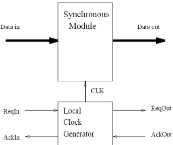
A stoppable clock can be used to design a globally asynchronous locally synchronous (GALS) architec- ture. Communication between modules is done asynchronously using request/acknowledge protocols while computation is done synchronously within the modules using a locally generated clock. The basic structure of such a module is shown in Figure 6. The module’s internal clock is stopped when it must wait for data to arrive from, or to be accepted by, other modules. If another module can request to communicate data to a synchronous module at arbitrary times as discussed above, the stoppable clock shown in Figure 4(b) is needed. If the synchronous unit determines when data is to be transferred to/from the other modules, there is no need for a ME element, since the decision to wait on asynchronous communication is synchronized to the internal clock. In this case, the stoppable clock shown in Figure 4(a) can be used. Numerous researchers have developed GALS architectures based on the idea of a stoppable clock. Some of the schemes such as those proposed in allow an asynchronous module to request to communicate data to a synchronous module at arbitrary times. The approach in is based on an asynchronous synchronizer called a Q-flop. This synchronizer receives a potentially unstable input and 9 a clock, and it produces a latched value and an acknowledgment when it has latched the value successfully.
Q-flops are used in Q-modules which are essentially synchronous modules clocked using a locally generated stoppable clock. These Q-modules are then interconnected asynchronously. The schemes proposed in assume that the synchronous unit determines when data is to be transferred to/from the asynchronous modules. Recently, a group from
IBM introduced a new GALS approach of the second kind called interlocked pipelined CMOS (IPCMOS). They implemented a test chip in a 0.18 μm 1.5 V CMOS process which consisted of the critical path from a pipelined floating-point multiplier. Their experimental results showed a typical performance of 3.3 GHz with a best-case performance of 4.5 GHz.
VII. Power Comparison
Simulations were performed on the extracted netlist of the converter of Figure.7.1 with a switch-level simulator to compare the power dissipation of the implemented A/D converter to a converter with two levels of 127 internal pipeline latches. To allow the switch-level simulator to evaluate the circuit, the clamping transistors, M5 and M6, in the preamplifier must be removed, and the analog input simulated by setting the 127 comparator inputs to binary values at each clock cycle. Figure 7.1(a) shows the breakdown of simulated power dissipation for the error reduction circuitry in both converters with a Nyquist frequency, full-scale sinusoidal input. The clock frequency is 80 MHz. The internally pipelined converter requires 3.48 times more power for the error reduction circuitry, with most of the increase in the power for the clock signal required for the internal latches.
Figure 7.2(b) shows the total power breakdown for the implemented converter and the internally pipelined converter with 254 internal pipeline latches. Due to the static current paths in the comparators and the removal of the clamping transistors, the comparators’ measured values are used. The simulated power dissipation for the digital portion of the circuit is within 5% of the measured values for the implemented converter. The total increase in total power for the internally pipelined converter is 1.24 times. Other converter designs, with lighter clock loads in the comparators, higher resolution, or deeper latch pipelines, will have even larger improvements.
Figure7.1. Power comparison (a)Error reduction circuit;(b) Total power dissipation
This paper has presented a review of the synchronization problem and strategies that have been developed to address it. It is crucial that designers know whether their selected strategy eliminates the probability of failure or simply minimizes it. In the latter case, a mean time between failure must be calculated to determine the reliability of the system. Finally, this paper presented two case studies of synchronization strategies and the techniques that are used to verify their correctness. As clock speeds increase, synchronization issues are becoming increasingly important, so such a formal verification approach to the analysis of synchronization strategies is essential to produce reliable systems in the future.
References:-
[1] David J. Rennie, Manoj Sachdev "Novel Soft Error Robust Flip-Flops in 65nm CMOS" IEEE TRANSACTIONS ON NUCLEAR SCIENCE, VOL. 58, NO. 5, OCTOBER 2011 [2] David Rennie, Member, DavidLi, Member, Manoj Sachdev, Bharat L. Bhuva,
[3]Srikanth Jagannathan, ShiJieWen, Richard Wong "Performance, Metastability, and Soft-ErrorRobustness Trade-offs for Flip-Flops in 40 nm CMOS" IEEE TRANSACTIONS ON CIRCUITS AND SYSTEMS—I: REGULAR PAPERS, VOL. 59, NO. 8, AUGUST 2012
[4] R. Baumann, ―Radiation-induced soft errors in advanced semiconductor technologies,‖ EEE Trans. Device Mater. Rel., vol. 5, no. 3,pp. 305–316, 2005.