Graphene Assisted Radiation Adjustable OAM Generator
Fuchun Mao1, Ming Huang1, *, Jialin Zhang2, Jingjing Yang1, and Tinghua Li1
Abstract—Graphene is increasingly being used in the design of electromagnetic devices. The resistivity of graphene can be adjusted via chemical potential tuning, which truly benefits the implementation of tunable and reconfigurable devices. This paper investigates the switch-like attribute of parasitic graphene surface used in a dipole operating at 0.39 THz. Further, a novel orbital angular moment (OAM) generator with radiation reconfiguration is proposed. Spiral beams carrying variety of OAM modes can be produced easily using the generator.
1. INTRODUCTION
Graphene has recently drawn massive amount of attention due to its unique semi-conductive, optical, chemical, mechanical, and thermal properties [1–3]. These features endow graphene with huge potential in various applications such as transistor [4, 5], optical modulator [6] and sensor [7]. The carrier concentration and chemical potential in graphene can be adjusted through chemical doping [8], optical injective [9], and electrostatic gating [10], which results in a tunable characteristic and makes graphene a favorite contender in electromagnetic applications from terahertz band to the visible [11]. However, current studies on graphene antenna are not yet abundant and confined to simple geometry like dipole, though a few of initial works have been presented.
The first study using graphene in antenna was presented in 2010, by adding a parasitic graphene layer between the gold arm and substrate, the authors were able to reconfigure the radiation of antenna operating at 0.12 terahertz [12]. Then, as a fundamental component in many antenna systems, the scattering, absorbance, and extinction cross section of graphene patch sticking to substrate were investigated numerically in [13]. Graphene as a real radiator rather than an auxiliary in antenna were presented in [14–16]. These antennas exploit plasmonic resonance in graphene, and allow high miniaturization, good omnidirectional radiation, as well as dynamic frequency tuning. While in [17], graphene monolayer was used as a high reactive impedance surface, and able to decrease lateral lobe. Transmission line parameters for surface plasmon polaritons (SPP) waves at graphene interface were analyzed through a tight-binding model [18, 19] and an equivalent circuit theory [20] respectively. In addition, optical antennas based on graphene rings with tunability and field enhancement in terahertz band were found by [21, 22]. These previous works are inspiring and not yet sufficient to dissuade researchers from subsequent exploring.
Considering the factor that few work has focused on the possibility of graphene to serve in an orbital angular momentum (OAM) generators who produce the so called electromagnetic vortexes from radio band to the visible, this paper is going to present a graphene assisted OAM generator, which is capable of radiation reconfiguration. The generator is composed of a circular array structure, which contains twelve independent graphene assisted dipole. All antennas and arrays are performed using the HFSS commercial electromagnetic simulation software.
Received 5 March 2015, Accepted 16 April 2015, Scheduled 21 April 2015
* Corresponding author: Ming Huang ([email protected]).
2. DIPOLE DESIGN
As a truly two-dimensional carbon crystal, graphene is described by its surface conductivityσ, governed by the Kubo formula [23]
σ= je 2 π ∞ 0 ε
∂fd(ε)
∂ε −
∂fd(−ε) ∂ε
dε− je
2(ω−j2Γ)
π
∞
0
∂fd(−ε)−∂fd(ε)
(ω−j2Γ)−(2ε/)2dε, (1)
wherefd(ε) = 1/[exp((ε−μc)/KBT) + 1] is the Feimi function, with KB the Boltzmann’s constant,μc the chemical potential, ε the energy and T the Kelvin temperature. Γ = 1/2τ is a phenomenological scattering ratio withτ the relax time. =h/2π is reduced Plank’s constant,ethe electron charge, and ωthe radian frequency. The first term in Equation (1) denotes the intraband’s contribution to σ, which can be computed as
σintra= −je 2K
BT
π(ω−j2Γ)
μc
KBT + 2 ln
exp
μc KBT
+ 1
. (2)
Accordingly, the second term denotes the contribution from interband, and can be evaluated as
σinter= −je 2
4π ln
2|μc| −(ω−j2Γ) 2|μc|+(ω−j2Γ)
. (3)
Since the chemical potential can be adjusted by bias voltage, graphene antennas are far superior to conventional metal antenna in the aspect of reconfigurability and tenability [15, 21]. The conductivity σ versus frequency behavior, as well as impedance z versus frequency, is shown in Figure 1, where σ = σintra +σintra, and z = 1/σ, with T = 300 K and Γ = 0.11 meV. Obviously, the conductivity increases with chemical potentialμc, while on the contrary the impedance decreases. More importantly, we find that resistivity of graphene is 49090−j18800 Ω·m and 5.672−j41.68 Ω·m at the frequencies around 0.39 THz, and the corresponding chemical potential isμc = 1 meV andμc = 0.5 eV, respectively.
(a) (b)
(c) (d)
Such drastic variation will put a significant impact on the dipole performance. These two different states of graphene will be defined as “on” and “off” in what follows.
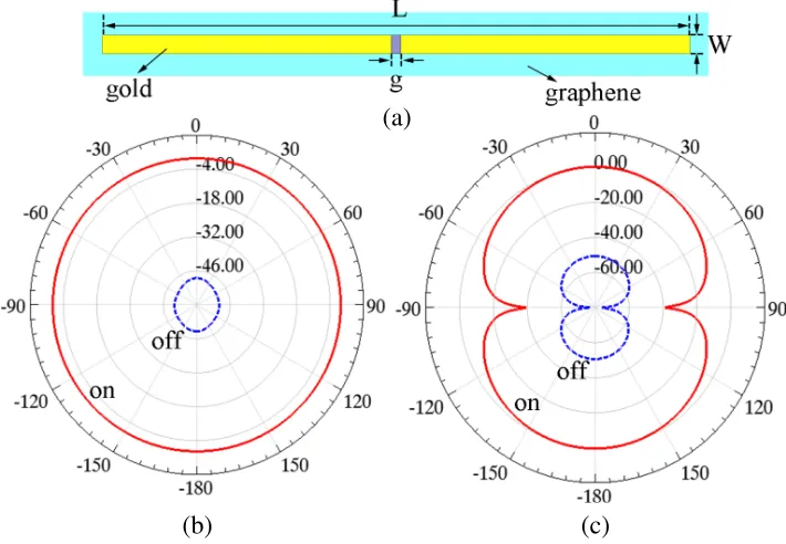
The structure of dipole is shown in Figure 2(a). Graphene monolayer with thickness 0.34 nm grows on a silica (εr = 4) substrate with thickness 0.3µm. Gold ribbons deposit on the graphene, with thickness 2µm. The length of dipole is L = 0.38λ = 318.06µm, width is W = 10µm. Gap between the two gold arms is g = 5µm. Considering an ideal scenario in aim of simulation that no material loss happen within graphene, we neglect the influence of imaginary part of impedance which indeed can be eliminated via applying the well-known impedance matching technique. The radiation patterns are shown in Figure 2(b) and Figure 2(c). The inner curve denotes the “off” state, while the outer denotes the “on” state. Obviously, the radiation differs about 50 dB both in E-plane and H-plane. In detail, in the “on” state, the radiation efficiency is 0.634, the max gain is 0.5 dB, while in the “off” state, the radiation efficiency and max gain is respectively only 9.2×10⁻⁶ and −48 dB. Thus the graphene film possesses a switch-like property. More importantly, when changing the chemical potential continuously, the efficiency and pattern of radiation will evolve simultaneously. On this basis, we will build a graphene assisted OAM generator in the rest of this paper.
(a)
(b) (c)
Figure 2. Graphene assisted dipole and its radiation patterns. (a) Structure diagram; (b)E-plane; (c) H-plane.
3. GRAPHENE ASSISTED OAM GENERATOR
OAM multiplexing technology has great potential in improving spectrum efficiency and communication security [24, 25]. It is expected to become the standard transmission method in future communication system. Thus the OAM generator with EM vortexes is a research hotspot in recent years [26–33]. The model of graphene assisted OAM generator is shown in Figure 3. It’s made up of 12 radiation elements placed along a circumference equidistantly, and the space orientations of elements parallel to thex-axis. Geometry structure of these elements is shown in Figure 2(a). The array radius is ra = λ, azimuthal difference between adjacent elements isα = 30◦. The exciting currents express asIn= exp(jlϕn), where l is the OAM mode number, and ϕn= (n−1)α is the phase ofnth element current. The array factor
for such array can be written as Fa = 12
1
Figure 3. Geometry model of graphene assisted OAM generator.
Figure 4. The distribution of phase andH-field intensity. From left to rightl varies from 0 to 5.
contains a phase dependent term ejlϕ, where ϕ is the azimuth. This implies the antenna array can be used to generate spiral beams carrying OAM [27, 28]. In addition, a reflective plane about λ/4 apart from the array plane is used in simulation.
The most conspicuous feature of an OAM beam is the spiral phase structure in wave front. Figure 4 shows the distribution of phase andH-field intensity with OAM mode numberl= 0, 1, 2, 3, 4, 5. Twists, at which the phase takes a sharp saltation from π to −π, are observed in the phase panels, and the number of twists exactly equals to the OAM mode l. Similar rotational distributions are found in the panels of intensity. For l= 0, all elements are fed by the same signal without phase delay. The energy of beam emits mainly in the bore sight direction. While for l= 0, a null where the intensity of field is extremely weak will appear in thezdirection. The distribution of intensity expands when mode number lbecomes larger. Obviously, the circular dipole array radiates hollow beams with helix phase structure, and can be used as an OAM generator.
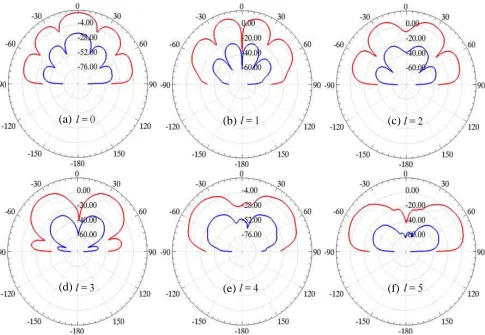
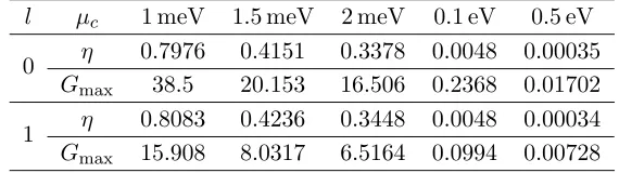
Figure 5 shows the radiation patterns inH-plane, where the OAM modelchanges from 0 to 5, and the azimuth equals 90◦. In each panel, the inner curve and outer curve are, respectively, performed at “on” state and “off” state. It can be seen that when l= 0, the main lobe lies atz axis, perpendicular to the array plane; while forl= 0, as mentioned before, a hollow arises at the shaft axis direction, and constructs a concentric circle profile of intensity distribution. Accompanying the swell of mode number l, the side lobe was inhibited gradually. Another trend is the decrease of propagation length since the power radiation becomes emanative. Comparing with the “on”case, maximum gain of generator decreases about 35 dB in the “off” state. More details in this tendency can be found in Table 1. This makes it possible to obtain switch operation of OAM generator by adjusting the chemical potential via gate voltage [34].
(a) (b) (c)
(d) (e) (f)
Figure 5. Radiation patterns in H-plane when all elements are in “on” state (inner pattern), or “off” state (outer pattern), where lvaries from 0 to 5 in order.
Figure 6. Distribution of phase and intensity ofH-field. Mode number isl= 1, the number of elements to be set at “off” state equidistantly is 6, 4, 3, 2 and 0 respectively from left to right.
(a) (b)
(c)
(d)
Figure 7. 2-D and 3D radiation patterns of generator, with mode numberl= 0, and chemical potential μc = 1 meV, 100 meV and 500 meV.
Table 1. Radiation efficiency and max gain under different chemical potential.
l μc 1 meV 1.5 meV 2 meV 0.1 eV 0.5 eV
0 η 0.7976 0.4151 0.3378 0.0048 0.00035 Gmax 38.5 20.153 16.506 0.2368 0.01702
1 η 0.8083 0.4236 0.3448 0.0048 0.00034 Gmax 15.908 8.0317 6.5164 0.0994 0.00728
In addition, the phase structure appears distortion, which will vanish if all elements operating at the same condition. In fact, graphene ribbons can further utilized in gain control within large region, which is testified by Table 1 and Figure 7.
Figure 7 shows the two-dimensional and three dimensional radiation patterns of the generator with mode number l = 0. Curves labeled by ‘c1’, ‘c2’ and ‘c3’ in panel (a) demonstrate the radiation of generator operating at μc1 = 1 meV, μc2 = 100 meV, and μc3 = 500 meV. The corresponding three dimensional patterns are shown in panels (b), (c), and (d). The ability of graphene in radiation control is observed. Since the decrease of radiation accompanies with the chemical potential increase, which can be changed easily via gate voltage, graphene layer in the proposed OAM generator have ability of adjusting the radiation and gain. This is believed to benefit the design of reconfigurable OAM generator.
4. CONCLUSIONS
ACKNOWLEDGMENT
This work was supported by the National Natural Science Foundation of China (Grant Nos. 61161007, 61261002, 61461052), the Specialized Research Fund for the Doctoral Program of Higher Education (Grant Nos. 20135301110003, 20125301120009), China Postdoctoral Science Foundation (Grant Nos. 2013M531989, 2014T70890), the Key Program of Natural Science of Yunnan Province (Grant No. 2013FA006), and the Seventh of Yunnan University Graduate Student Scientific Research Project (Grant No. ynuy201443).
REFERENCES
1. Geim, A. K., “Graphene: Status and prospects,” Science, Vol. 324, No. 5934, 1530–1534, 2009. 2. Allen, M. J., V. C. Tung, and R. B. Kaner, “Honeycomb carbon: A review of graphene,”Chemical
Reviews, Vol. 110, No. 1, 132–145, 2009.
3. Cooper, D. R., B. D’. Anjou, N. Ghattamaneni, B. Harack, M. Hilke, A. Horth, N. Majlis, M. Massicotte, L. Vandsburger, E. Whiteway, and V. Yu, “Experimental review of graphene,”
International Scholarly Research Notices, Vol. 2012, 2012.
4. Lin, Y.-M., C. Dimitrakopoulos, K. A. Jenkins, D. B. Farmer, H.-Y. Chiu, A. Grill, and Ph. Avouris, “100-GHz transistors from wafer-scale epitaxial graphene,” Science, Vol. 327, No. 5966, 662–662, 2010.
5. Wu, Y., Y. Lin, A. A. Bol, K. A. Jenkins, F. Xia, D. B. Farmer, Y. Zhu, and P. Avouris, “High-frequency, scaled graphene transistors on diamond-like carbon,”Nature, Vol. 472, No. 7341, 74–78, 2011.
6. Ming, L., X. B. Yin, and X. Zhang, “Double-layer graphene optical modulator,” Nano Letters, Vol. 12, No. 3, 1482–1485, 2012.
7. Francescato, Y., V. Giannini, J. J. Yang, M. Huang, and S. A. Maier, “Graphene sandwiches as a platform for broadband molecular spectroscopy,” ACS Photonics, Vol. 1, No. 5, 437–443, 2014. 8. Liu, H. T., Y. Q. Liu, and D. B. Zhu, “Chemical doping of graphene,” Journal of Materials
Chemistry, Vol. 21, No. 10, 3335–3345, 2011.
9. Fang, Z. Y., Y. M. Wang, Z. Liu, A. Schlather, P. M. Ajayan, F. H. L. Koppens, P. Nordlander, and N. J. Halas, “Plasmon-induced doping of graphene,” Acs Nano, Vol. 6, No. 11, 10222–10228, 2012.
10. Ashkan, V. and N. Engheta, “Transformation optics using graphene,”Science, Vol. 332, No. 6035, 1291–1294, 2011.
11. Perruisseau-Carrier, J., “Graphene for antenna applications: Opportunities and challenges from microwaves to THz,” IEEE Antennas and Propagation Conference (LAPC), 2012, 1–4, Loughborough, 2012.
12. Dragoman, M., A. A. Muller, D. Dragoman, F. Coccetti, and R. Plana, “Terahertz antenna based on graphene,”Journal of Applied Physics, Vol. 107, No. 10, 104313, 2010.
13. Llatser, I., C. Kremers, A. Cabellos-Aparicio, J. M. Jornet, E. Alarc´on, and D. N. Chigrin, “Graphene-based nano-patch antenna for terahertz radiation,” Photonics and Nanostructures-Fundamentals and Applications, Vol. 10, No. 4, 353–358, 2012.
14. Tamagnone, M., J. S. Gomez-Diaz, J. R. Mosig, and J. Perruisseau-Carrier, “Analysis and design of terahertz antennas based on plasmonic resonant graphene sheets,” Journal of Applied Physics, Vol. 112, No. 11, 114915, 2012.
15. Tamagnone, M., J. S. Gomez-Diaz, J. R. Mosig, and J. Perruisseau-Carrier, “Reconfigurable terahertz plasmonic antenna concept using a graphene stack,” Applied Physics Letters, Vol. 101, No. 21, 214102, 2012.
17. Dragoman, M., M. Aldrigo, A. Dinescu, D. Dragoman, and A. Costanzo, “Towards a terahertz direct receiver based on graphene up to 10 THz,” Journal of Applied Physics, Vol. 115, No. 4, 044307, 2014.
18. Jornet, J. M. and I. F. Akyildiz, “Graphene-based nano-antennas for electromagnetic nanocommunications in the terahertz band,”2010 Proceedings of the Fourth European Conference
on IEEE Antennas and Propagation (EuCAP), 1–5, 2010.
19. Jornet, J. M. and I. F. Akyildiz, “Graphene-based plasmonic nano-antenna for terahertz band communication in nanonetworks,” IEEE Journal on Selected Areas in Communications, Vol. 31, No. 12, 685–694, 2013.
20. Tamagnone, M. and J. Perruisseau-Carrier, “Predicting input impedance and efficiency of graphene reconfigurable dipoles using a simple circuit model,” arXiv preprint arXiv:1402.1527, 2014.
21. Liu, P., W. Cai, L. Wang, X. Zhang, and J. Xu, “Tunable terahertz optical antennas based on graphene ring structures,”Applied Physics Letters, Vol. 100, No. 15, 153111, 2012.
22. Filter, R., M. Farhat, M. Steglich, R. Alaee, C. Rockstuhl, and F. Lederer, “Tunable graphene antennas for selective enhancement of THz-emission,” Optics Express, Vol. 21, No. 3, 3737–3745, 2013.
23. Hanson, G. W., “Dyadic Green’s functions and guided surface waves for a surface conductivity model of graphene,”Journal of Applied Physics, Vol. 103, No. 6, 064302, 2008.
24. Wang, J., J. Y. Yang, I. M. Fazal, N. Ahmed, Y. Yan, H. Huang, and A. E. Willner, “Terabit free-space data transmission employing orbital angular momentum multiplexing,” Nature Photonics, Vol. 6, No. 7, 488–496, 2012.
25. Bozinovic, N., Y. Yue, Y. Ren, M. Tur, P. Kristensen, H. Huang, and S. Ramachandran, “Terabit-scale orbital angular momentum mode division multiplexing in fibers,”Science, Vol. 340, No. 6140, 1545–1548, 2013.
26. Barbuto, M., F. Trotta, F. Bilotti, and A. Toscano, “Circular polarized patch antenna generating orbital angular momentum,”Progress In Electromagnetics Research, Vol. 148, 23–30, 2014. 27. Mohammadi, S. M., L. K. Daldorff, J. E. Bergman, R. L. Karlsson, B. Thid´e, K. Forozesh,
and B. Isham, “Orbital angular momentum in radio — A system study,” IEEE Transactions on Antennas and Propagation, Vol. 58, No. 2, 565–572, 2010.
28. Thid´e, B., H. Then, J. Sj¨oholm, K. Palmer, J. Bergman, T. D. Carozzi, and R. Khamitova, “Utilization of photon orbital angular momentum in the low-frequency radio domain,” Physical Review Letters, Vol. 99, No. 8, 087701, 2007.
29. Tamburini, F., E. Mari, A. Sponselli, B. Thid´e, A. Bianchini, and F. Romanato, “Encoding many channels on the same frequency through radio vorticity: First experimental test,”New Journal of Physics, Vol. 14, No. 3, 033001, 2012.
30. Rui, G., R. L. Nelson, and Q. Zhan, “Beaming photons with spin and orbital angular momentum via a dipole-coupled plasmonic spiral antenna,”Optics Express, Vol. 20, No. 17, 18819–18826, 2012. 31. Zhu, J., X. Cai, Y. Chen, and S. Yu, “Theoretical model for angular grating-based integrated
optical vortex beam emitters,” Optics Letters, Vol. 38, No. 8, 1343–1345, 2013.
32. Bouchard, F., H. Mand, M. Mirhosseini, E. Karimi, and R. W. Boyd, “Achromatic orbital angular momentum generator,”New Journal of Physics, Vol. 16, No. 12, 123006, 2014.
33. Marrucci, L., C. Manzo, and D. Paparo, “Optical spin-to-orbital angular momentum conversion in inhomogeneous anisotropic media,”Physical Review Letters, Vol. 96, No. 16, 163905, 2006.