Achieving Electrothermal Stability in Interconnect
Metal During ESD Pulses
Timothy J. Maloney
Intel Corporation Santa Clara, CA 95054 USA(408)765-9389, [email protected]
Lei Jiang, Steven S. Poon, Krishna B. Kolluru, and AKM Ahsan
Intel CorporationHillsboro, OR 97124 USA
Abstract—A feedback model of on-chip interconnect metal heating during electrostatic discharge (ESD) pulses predicts a temperature waveform and its stability given a heat source function and a thermoelectric circuit model or thermal impulse response Z(t). The pulse delivery circuit influences those conditions along with materials and layout. Z(t) can be extracted from pre-silicon modeling (e.g., finite element) or from post-silicon transmission line pulse (TLP) response, then applied to any ESD pulse conditions. For metal lines embedded in a patterned matrix of inactive metal lines at adjoining levels, pulses produce temperatures converging to a constant value, so the related time constants allow thermal impedance Z(t) to be deduced and thermal properties of the materials checked.
Keywords-thermal feedback, ESD; IC metal; complex thermal impedance; TLP; HBM; CDM; thermal impulse response
I. INTRODUCTION
Resistive self-heating of interconnect metal during ESD pulses has a long history [1-5 and references therein], including the adiabatic approximation, but for longer pulses such as Human Body Model (HBM), the conduction of heat by surrounding oxide is no longer negligible. Moreover, heat conduction by inert metal elements on the other side of surrounding oxide may amount to, and be modeled as, a heat sink on the time scale of the ESD event. With ever-shrinking geometries for integrated circuits, the worst-case adiabatic approximation of earlier times is no longer acceptable; these heat-conducting effects need to be evaluated and invoked in design and layout validation.
The one-dimensional (1-D) heat flow equation [6,7] is the same differential equation as for an RC electrical transmission line, namely
t
V
RC
x
V
∂
∂
=
∂
∂
2 2
. (1) The heat flow equation was connected to such distributed electrical lines having negligible inductance back in the 19th century [7]. For heat flow, temperature T is analogous to voltage V; 1/K per unit area (thermal conductivity K in W/cm-°C) is like resistance per unit length R; and ρCp=Cv or volume heat capacity times unit area (ρ in gm/cm3 and Cp in J/gm-°C) is like capacitance per unit length C. Accordingly,
in this work we aim to use various 1-D RC transmission line models along with lumped RC elements to solve heat flow boundary value problems for cases when integrated circuit (IC) metal interconnect undergoes electrostatic discharge (ESD) pulse testing. Resistive self-heating will be expressed as a feedback element, and thermal stability conditions will be examined. We will analogize units as follows:
Volts°C, temperature (usually a ∆T from room T) Amps Watts
Coulombs Joules
Ohms thermal impedance °C/W Farads Joules/°C
IC technology has reached a point where leadway metal that will undergo ESD stress is partitioned into many small parallel lines, with the result that temperature in the metal cross-section is now virtually uniform. We will see that the metal temperature is controlled by its heat capacity and out-diffusion of heat from these metal segments, and the heat flow can be decomposed into parallel 1-D paths. The resulting thermal input impedance Z(s) determines the metal temperature if input heat flow (“current”) is known. The electrical analog is extended further by capturing metal self-heating as positive feedback, plus any additional effects of temperature rise on the heat flow (current) function, negative feedback in the case of TLP.
II. 1-D INTERCONNECT MODELS WITH THERMAL FEEDBACK
A. Setting Up the Thermal Impedance Function
Distributed R-C heat flow paths will be represented by t-line segments having characteristic impedance Z0 and propagation constant γ as from standard texts on RLGC lines, where for us, G=L=0 [8]:
p
C
sK
sC
R
Z
ρ
1
0
=
=
(2a)
K
C
s
RCs
ρ
pγ
=
=
Note that these quantities depend on complex frequency s=σ+jω. The thermal impedance and impulse response of a semi-infinite solid (silicon, for example), would simply be Z0 (scaled by area), and its temperature response to a step function heat source I0/s amounts to finding a Laplace Transform of s-3/2, proportional to t1/2 [9]. This is the famous Wunsch-Bell result [10]. Their results were obtained with “effective” material parameters over a given temperature range, and of course that remains a consideration when working with these linearized models.
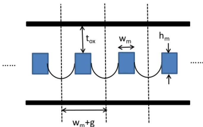
The metal test structure cross-section as pictured in Figure 1, for a 22 nm process, represents many of today’s product leadway metal schemes. Current runs on a set of minimum size Metal-5 wires that extend far to the right and left of those shown. Thus metal heats uniformly and and has much more metal-oxide interfacial area than previous IC generations. In the adjacent damascene metal layers of this test structure there is “dummy” metal and via as shown, unconnected to the M5 line under test but typical of product that will have unrelated signals, or dummies of its own to meet process design rules. Thus the nearby inert metal forms a substantial heat sink, although isolated by thermally resistive interlayer dielectric (ILD). Even so, with short ESD pulses of no more than a few hundred nanoseconds, these adjacent layers can be considered a single thermal resistance to ground ZL, and the ILD an RC line terminated by ZL. The heating source and sink is, in effect, applied across one dimension, with the wide grid of metal lines a kind of heat slab as treated in classic texts [6]. As the metal thickness is a major fraction of the ILD thickness, there is also the heating of the interstitial oxide between metal lines to consider. At minimum, the heat capacity of the oxide should be included with that of the metal to form a larger capacitor. But fortunately, this volume of ILD can be seen as a lateral (although very short) R-C line, with an elegant open-circuit boundary condition representing the midpoint between metal segments as pictured in Figure 2. Z(s) is now a lumped capacitor for the metal and two R-C lines in parallel, as pictured in Figure 3.
Most of the experimental work reported here was done on two test structures called Patterns C and D. The schematic cross-section as in Fig. 1 resembles Pattern C, with narrow gap gC (see Fig. 2) between metal lines. On Pattern D, gD=2gC. Both patterns are 211 µm long and have 1 µm2 metal cross section, so Pattern D is wider.
Figure 1. Interconnect lines (M5, middle) in a test pattern resembling product. Heat flows through ILD to “dummy” metal and vias on adjacent metal layers.
Figure 2. M5 interconnect line close-up showing temperature gradient zero boundary condition between lines, plus metal and oxide dimensions. Gap spacing g varies for the test patterns as discussed. Line length lm=211 µm.
Figure 3. Thermal impedance model of interconnect, fed by power function P(t). Impedances Z01, Z02 go inversely with heat slab areas 2lm(wm+g)n and
2nlmhm respectively, n the number of metal lines (n>100 for Patterns C and D).
The model of Fig. 3 uses two 1-D models to approximate a 2-D situation, but this is believed to be fairly good for various reasons, among them the lateral and vertical space occupied by the metal in the unit cell as shown in Fig. 2. Solutions of the transient cylindrical heat flow problem, acquired by one of us (SSP) in extensive work internal to Intel, are found to match with Fig. 3 for short times, when the wires are independent, if the right line impedances are chosen. Calculations like this provide a path to cross-check our thermal impedance impulse response functions, to be discussed later.
B. Modeling of Feedback Phenomena
Before we continue with computing the thermal impedance Z(s), we should complete the thermal circuit model by including feedback effects. Foremost among these is self-heating of the metal line. Its resistance is
))
(
1
(
)
(
t
R
0T
t
R
=
+
α
, (3)where R0 is the metal resistance at reference temperature T0, T(t) the temperature above T0, and α the (positive) temperature coefficient (tempco) of the metal (0.0025/°C for Cu metal in this work). For an independent current source, the power function P(t)=I(t)2R(t) is defined once T(t) is computed from the thermal impedance. I(t) is nearly always independent for HBM ESD because the source impedance is 1500 ohms,
M5
w
m+g
……
……
w
mt
oxhm
Cmetal
Z01, γoxtox
ZL Z02, γoxg/2
while for the Charged Device Model (CDM) at ≥20 ohms or TLP (usually 50 ohms), there could be a negative feedback effect due to resistance rise. In any case, current source is a worst case to consider when predicting metal heating. For an independent current source, if P(t)=I2(t)R(t)=P0(t)(1+αT(t)), T(s)=P(s)Z(s), then
)
(
*
)]
(
)
(
[
)
(
*
)
(
)
(
t
P
0t
Z
t
T
t
P
0t
Z
t
T
=
+
α
, (4)where * is the convolution operator and Z(t) the impulse response, transformed from Z(s). T(t) generally has to be solved iteratively, but a circuit simulator with a “behavioral” current source in the mixer-based feedback arrangement of Figure 4a is sufficient once the functions are known. Eq. (4) can also be expressed as a feedback-like equation,
[
]
)
(
)
(
*
)
(
)
(
1
)
(
*
)
(
)
(
0 0t
T
t
Z
t
P
t
T
t
Z
t
P
t
T
α
−
=
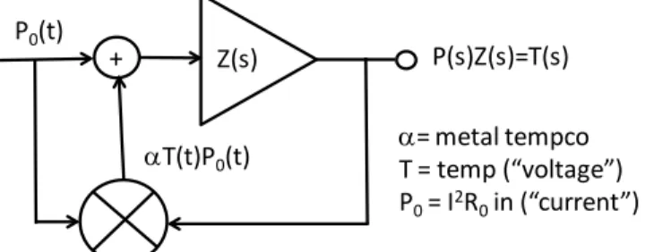
. (5) This is still an implicit equation for T(t) because of T(t)P0(t) being tied up in convolution with Z(t), but can inspire a good starting function for T(t). But convergence is fast from nearly any starting point. The second denominator term of (5) expresses the Nyquist criterion for stability, although infinite energy is needed for it to reach -1. Still, it reveals how much feedback is going on, negative or positive.Figure 4a. Feedback model of interconnect metal heating for an independent current source I(t) that produces initial heat source P0(t)=I2(t)R0.
Figure 4b. General feedback model of interconnect metal heating. For TLP, P0(t) is a constant P0 but total P(t) is modified by the feedback network.
More generally, the feedback from T(t) affects the current source, which has some output impedance. This is the case with TLP for our test patterns with R0=10.4 ohms, as temperatures rise to α∆T=2 or 3. TLP has a long history of being used for pulsed metal studies [11, 1-5]. Solving the
network for TLP with step V0/s and source Zs=50 ohms is fairly simple; the initial power source is
(
)
20 0 2 0 0 0
50
)
(
+
=
=
R
R
V
P
t
P
, (6)and the feedback network FB(t) pictured in Figure 4b is
−
+
+
+
=
1
50
)
(
1
)
(
1
)
(
2 0 0 0R
t
T
R
t
T
P
t
FB
α
α
. (7)
The negative feedback of the TLP system grows with
αR0T(t) and becomes dominant as the resistance goes above 50 ohms and the TLP becomes more of a voltage source. Again, the behavioral source of a circuit simulator can handle the more generalized P0(t)+FB(t) function. For an approximation, Eq. (7) can be expanded to give an effective α,
+
+
−
=
0 050
50
R
R
effα
α
, (8)where the next terms depend on T. This reduced value of α can be used in estimates but Eq. (7) and an iterative solution is generally needed for precision.
When a TLP pulse ends at constant temperature, (7) tells us there must be a heat flow balance such that
th final final th final final
Z
R
T
R
T
P
Z
P
T
2 00 0 0 0
50
1
1
+
+
+
=
=
α
α
. (9)
Pfinal comes from the TLP electrical data, thus giving Z0th at numerous power levels, using α to measure the metal temperature in situ. It is then possible to predict thermal margin as given by αeffP0Z0th, but soon we will see even more information extracted from TLP data. Note that the pulse output impedance and feedback circuit, expressed by Eqs. (7-9), participate along with material properties to determine the maximum temperature Tmax as obtained by iterative solution of Eqs. (4-5). Thus the relative values of R0 and 50 ohms (or other choice for Zs) are crucialto electrothermal stability. The same physics in Eq. (9) also leads to
th eff th th final final
Z
P
Z
P
Z
P
T
0 0 0 0 01
−
α
=
=
. (10)Now the bracketed term in (9) is seen as a multiplier, leading to αeff and the magnitude and sign of the feedback.
+ Z(s)
αT(t)P0(t)
P0(t)
P(s)Z(s)=T(s)
α= metal tempco T = temp (“voltage”) P0= I2R0in (“current”)
+
Z(s)
FB(t)
P
0(t)
Convolve
P(t)*Z(t)=T(t)
T(t)
Note that Eqs. (4-10) also suggest measuring Z(s)⇔Z(t) by deconvolving the TLP in situ T(t) and P(t) data, whereupon the temperature profiles and Tmax can be examined for any ESD pulse. We will return to this later.
III. FINDING IMPULSE RESPONSE IMPEDANCE FUNCTIONS We have several ways to arrive at the thermal impedance impulse response Z(t), aiming at subsequent use in the feedback equation (4) for T(t). Before any structures are built on-chip, materials parameters can be used in the circuit model of Fig. 3 to estimate a Z(t) through step response or impulse response, although termination ZL is likely to be an R-C combination. As we will see, other studies can guide selection of ZL. In addition, finite element modeling (FEM) can be used to simulate the entire structure or a unit cell with appropriate boundary conditions, again by input of a constant heat flow or an impulse, without yet considering metal tempco or self-heating. These pre-silicon evaluation methods will be discussed next; post-silicon methods follow that and offer a simplified thermal circuit model that matches information from the TLP waveforms.
A. Pre-silicon Modeling
The finite element method was used to study a constant 8.44W step input at the M5 metal wires as in Fig. 1 (Pattern C, with tight spacing as described in Section II), with resulting temperature profile after 200 nsec shown by the false colors in Figure 5. Since the upper (M6 and above) heat sink is ultimately floating and therefore capacitive, while M1-M4 have silicon below it, the temperature differences of top and bottom after 200 nsec are not surprising. A refined circuit model of Fig. 3 would have two symmetric terminated lines but with ZL capacitive and primarily resistive, respectively, for the upper and lower lines.
Figure 5. FEM result after 200 nsec for 8.44W step input to M5 lines (red) of Pattern C, as in Figs. 1-2 and Section II. Upper metal is thermally floating.
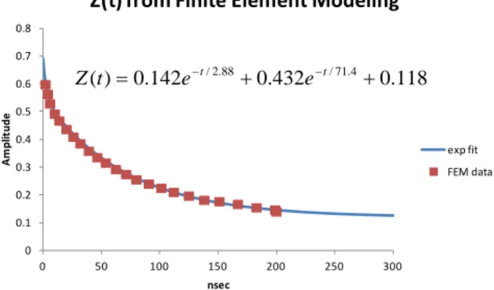
Z(t) is derived from the finite element step response by differentiating the T(t) curve (normalized to 1W) for a typical location in the geometric center of the test structure, and appears in Figure 6 along with a curve fit using exponential functions as shown. The step response on the 200 nsec scale ends with a ramp, suggesting capacitive termination on this time scale, so there is a positive offset in the impulse response.
But we expect that for most ESD events, the capacitive offset will have its main effect on the tail of the temperature decay, and only mildly affect Tmax.
Figure 6. Impulse response Z(t) (°C/W-nsec) derived from FEM result on structure as in Fig. 5. Analytic fit as shown; time in nsec. Offset corresponds to 8.44 nF (nJ/°C) of capacitance; rest of Z(t) integrates to 31.3Ω (°C/W).
B. Post-silicon Modeling Using TLP Data
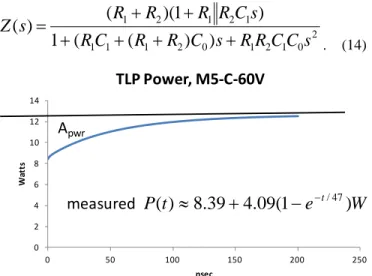
TLP measurements are very revealing about Z(t) because of the simplicity of the pulse and circuit, and because the resulting waveforms can often be analytically described. Because of the self-heating of the metal due to α, the final power function P(t) for Pattern C at 60V increases from a baseline of 8.39W to 12.48W, in exponential approach fashion, as in Figure 7a. Thus the Elmore Delay [12, 13] as deduced from Apwr leads to the time-dependent expression on Fig. 7a and the following expression in the s-domain:
)
47
1
(
09
.
4
39
.
8
)
(
s
s
W
s
W
s
P
+
+
=
. (11) The time constant is in nsec and s is in GHz, as will be the case below. Next, the temperature data in Figure 7b (deduced from the TLP response voltage, measuring T with the dc-measured
α=0.0025 for this layer of Cu metal) leads to the exponential approach expression as shown, which corresponds to
)
58
1
(
440
)
(
s
s
C
s
T
+
=
. (12) But the definition of thermal impedance, as reviewed in Section II, is P(s)Z(s)=T(s), so from these measured waveforms we can deduce that
Ω
+
+
+
=
)
58
1
)(
6
.
31
1
(
47
1
26
.
35
)
(
s
s
s
s
Z
or °C/W. (13) Note that Tfinal of 440°C corresponds to Eqs. (9-10) with Z0th=35.26 °C/W and Pfinal=12.48W. With two poles, a zero, and a scaling factor, Eq. (13) points to the four component values in the circuit of Figure 8, since
0 0.1 0.2 0.3 0.4 0.5 0.6 0.7 0.8
0 50 100 150 200 250 300
Am
pl
itu
de
nsec
Z(t) from Finite Element Modeling
exp fit FEM data 118 . 0 432
. 0 142
. 0 )
2 0 1 2 1 0 2 1 1 1
1 2 1 2
1
)
)
(
(
1
)
1
)(
(
)
(
s
C
C
R
R
s
C
R
R
C
R
s
C
R
R
R
R
s
Z
+
+
+
+
+
+
=
. (14)
Figure 7a. Measured power vs. time over a 60V TLP pulse on Pattern C; normalized Apwr gives time constant of 47 nsec for exponential approach.
Figure 7b. Measured temperature over the same pulse as Fig. 7a, where normalized AC gives time constant of 58 nsec. Calculated curve comes from
applying the full feedback model and Eq. 7; see text.
Figure 8. Thermal circuit model for Pattern C, with impedance corresponding to Eq. (14) and values as solved with TLP data by comparing Eqs. (13) and (14).
Fig. 8 contains much physical insight. The thermal grounding is fairly good, with large C1 and small R1 contributing to the poles and zero. Meanwhile, C0 = 1.1 nJ/°C is only 5% above what is calculated from the material properties of Cu (211 µm3, for 728 pJ/°C heat capacity) and the “gap” oxide (open-circuited Z02 line in Fig. 3), plus 1/3 of the “conduction” oxide Z01 line terminated by ZL. Because ZL is low, Z01 is almost a tanh (shorted) line for its impedance Zin, meaning that admittance Yin=Y01coth(γtox), Y01=1/Z01. Using
Eqs. (2) for Z and γ, the coth line can then be approximated by a parallel R-C circuit, using
+
+
=
3
1
)
coth(
x
x
x
[9]. (15) Thus the s-term of the estimated admittance is 1/3 of the conduction oxide thermal capacitance. This is what gives 5% agreement with estimated ρCp values when lumped in with C0. Were it not lumped with C0, the circuit model would have another pole and zero, which are hard to discern from the TLP waveforms. The oxide conductivity K is expressed in R2=32.7
°C/W and is a believable value, although perhaps optimistic. The FEM response (Fig. 6) has a baseline of 31.3Ω (°C/W), found through integration, but with the offset due to the capacitive sink (8.44 nF, or nJ/°C), that estimate for the first 200 nsec would be 55 °C/W. The news that either the oxide K is higher, or that the real structure has a better heat sink than the model, is of course good.
The time domain expression for Z(t) as derived from TLP data, corresponding to Eq. (13), is found using Heaviside inversion of the Laplace Transform [9] with Mathematica, and is shown in Figure 9 along with a plot. It has the same general time scale and range as the FEM-derived Z(t) of Fig. 6, but different shape, so it will be interesting to compare ESD convolutions. Fig. 7b suggests a possible final temperature ramp, indicating some offset capacitance resembling Fig. 6; that was not included in the model but could be done easily.
Figure 9. Thermal impulse response Z(t), as derived from TLP data and inversion of Eq. (13) to the time domain. Time constants in nsec.
The calculated curve fit in Fig. 7b is not a plot of the expression (12) for T(s) that was estimated for the measured data in pursuit of Z(s). The curve was found by applying the resulting Z(t) (Fig. 9) and starting TLP power P0(t)=P0=8.44W to the full feedback expression with FB(t) as in Eq. 7, and solving, iteratively, for T(t). With a trial T(t) function of P0Z(t), convergence to the final self consistent T(t), as plotted, happens after two or three iterations. In this way all positive feedback effects of α=0.0025, and negative feedback effects of 50-ohm TLP with R0=10.4 ohms, are considered. Negative feedback gradually increases over the time of the pulse as total wire resistance rises, but Eq. (7) captures that. The method cross-checks many aspects of the Z(t) derivation procedure 0
2 4 6 8 10 12 14
0 50 100 150 200 250
W
atts
nsec
TLP Power, M5-C-60V
A
pwrmeasured
P
(
t
)
≈
8
.
39
+
4
.
09
(
1
−
e
−t/47)
W
AC
calculated from Eq. (7)
C
e
t
T
(
)
≈
440
(
1
−
−t/58)
measured
P(t) ⇔P(s) C0
C1
R1 R2
C0= 1.1 nJ/°C (metal + oxide)
R2= 32.7 °C/W (oxide)
C1 = 20 nJ/°C
R1= 2.52 °C/W 0
0.1 0.2 0.3 0.4 0.5 0.6 0.7 0.8 0.91
0 50 100 150 200
Am
pl
itu
de
nsec
Z(t) from TLP data (°C/nJ)
)
00718
.
0
0185
.
0
(
26
.
35
)
(
t/31.6 t/58e
e
t
described above, and builds confidence in further use of Z(t). Since α is also used for thermometry, this method does not independently and precisely confirm α=0.0025 (measured for the process at dc) but clearly the data are consistent with this value, and the rise in power over time during the pulse indicates a substantial tempco.
Pattern C data at 70 and 80V TLP were also analyzed and compared with the above 60V TLP case. “Local” RC values (C0, R2) were always within 10% of those in Fig. 8. With Tfinal of 645 and 1072°C for 70-80V, respectively, the expected slight degradation of thermal properties (K, ρCp) took place, causing R2 to rise 10% and C0 to drop 10% for the 80V case. The heat sink (R1, C1) degradation seemed more pronounced for high temperatures, but typical ESD pulses (HBM, CDM) will not produce such a large-volume ∆T. Z(t) as shown in Fig. 9 should represent most ESD conditions of interest.
As a final note in this section, Pattern D, with wider oxide gap spacing gD=2gC as described in Section II, was also measured on TLP at 60V. As expected, Pattern D showed lower Z0th, 23.2°C/W, which broke out into R2=21.87 and R1=1.33°C/W. C0 became 1.53 nJ/°C and C1, 29.48 nJ/°C. Tfinal was 255 °C for Pattern D, with about the same starting power, 8.24W, at 60V. Everything scaled as expected with area, particularly the heat sink constants C1 and R1.
IV. HBM AND CDM TEMPERATURE STUDIES The Z(t) functions can be convolved with power functions derived from HBM and CDM current sources and then applied to Eqs. (4-5) to find the temperature waveform. As stated above, HBM with 1500 ohms source impedance will usually be an almost perfect current source and will not react to metal line resistance increase during the pulse. With typically 20-25 ohms spark resistance, CDM may well react to resistance rise, but the FB(t) function is more complicated than it is for TLP (Eq. (7)), as current is delivered by an L-C network, along with spark R, in the very simplest model. Although approximations could be made, we will study the CDM from a pure current source. This is a worst case, yet one that realistically represents heat flow in, for example, a short line section of interest where the metal is constricted.
Figure 10. Thermal impulse response Z(t), with TLP data augmented by a gradual increase to adiabatic 1.37 °C/nJ, using a heat diffusion length model.
The Z(t) function was derived and measured without much regard for very short times (low nanoseconds), where the impulse response is known to start out with adiabatic heating of the metal (1.37 °C/nJ for 211 µm3 of Cu as discussed earlier). This puts a ceiling on Z(0) of 1.37, but our TLP Z(t) function reaches only about 0.9 and the FEM function only 0.7 (Figs. 6, 9). Thus, particularly for CDM, it is advisable to put in a gradual fit of Z(t) to its presumed low time-scale values, just to be safe. At first, the wires are all independent, so the heat spreading into the oxide can follow a “heat sheath” model [3], whereby heat spreads into a volume of oxide set by √Dt, D the heat diffusivity of the oxide. A fit to the experimental TLP Z(t) for Pattern C is shown in Figure 10, where the merge with the measured curve as shown is perfect if 2Dt (beveled corners) is taken as the corner area of the sheath. The same thing was done to augment the FEM Z(t) for low times, with fitting enabled by optimistic adjustments to material parameters.
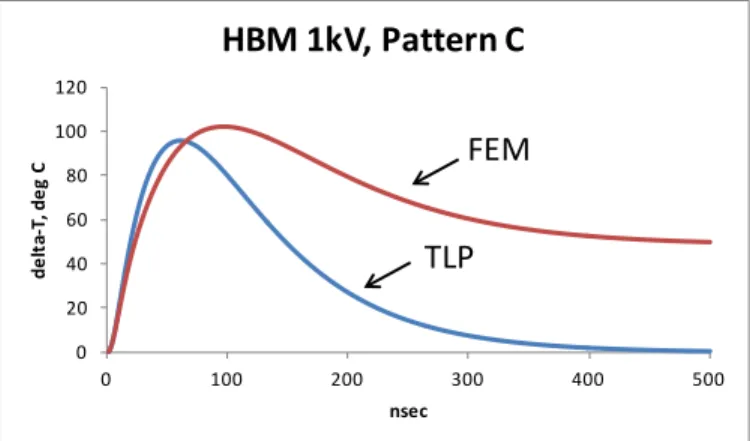
Figure 11a. Temperature response to 1kV HBM pulse for the two derived Z(t) functions. Peak temperature rise of ~100°C is found for each.
Figure 11b. Temperature response to 2kV HBM pulse for the two derived Z(t) functions. Peak temperature rise of >700°C is found for each.
The heating pulse P0(t) for HBM comes from I2(t)R0, where I(t) is a standard double-exponential HBM pulse based on test voltage. We will use the standard 1500 ohm, 100 pF values of R and C for HBM, and use L=6µH to give a 7 nsec 10-90% rise time. This works out to a P0(t) for 1kV HBM test voltage of
0 0.2 0.4 0.6 0.8 1 1.2 1.4 1.6
0 5 10 15 20
Am
pl
itu
de
nsec
Z(t) at short times
Dt model TLP data
Dt
model
adiabatic
0 20 40 60 80 100 120
0 100 200 300 400 500
de
lta
-T,
d
eg
C
nsec
HBM 1kV, Pattern C
FEM
TLP
0 100 200 300 400 500 600 700 800 900
0 100 200 300 400 500
de
lta
-T,
d
eg
C
nsec
HBM 2kV, Pattern C
FEM
+
+
−
=
e
−te
− te
+ tt
P
6015 201 60
15 201 4 /
0
2
201
1040
)
(
. (16) Temperature profiles for 1kV and 2kV HBM on our Pattern C lines are shown in Figures 11a and 11b. Convolution was done with free software for Excel [14], and iteration required only a few steps per curve. As expected, the two Z(t) functions predict about the same peak temperature, and the capacitive heat sink of the FEM-derived Z(t) results in a long decay tail and residual temperature, but with no evidence of harming the metal. The TLP heat sinking, reflecting real silicon that is even much thicker than that of a packaged die, looks more than sufficient for cooling between pulses during automated HBM testing. Finally, the feedback effect of the metal heating with positive tempco is evident—compared to 1kV, the 2kV pulse delivers 4 times the P0(t) to a fixed resistor, but the peak temperature of this metal is more than 7 times higher, ∆T going from about 100°C to over 700°C. This is still short of the Cu melting point of about 1069°C.
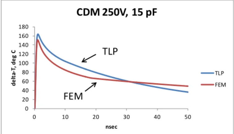
Figure 12a. Temperature response to 250V CDM pulse for the two derived Z(t) functions, Pattern C. Peak temperature rise is 150-160°C.
Figure 12b. Temperature response to 500V CDM pulse for the two derived Z(t) functions, Pattern C. Peak temperature rise is 1200-1300°C, with temporary melting of the Cu lines.
CDM temperature profiles were done using a critically damped CDM current waveform, having double time constants at 300 psec and 15 pF effective capacitance. Charge delivered was therefore 3.75 and 7.5 nC, with Ipeak of about 4.5 and 9A, for 250V and 500V respectively. Temperature profiles are shown in Figures 12a and 12b. Again the peak temperatures
are not too different, and the FEM Z(t) gives the expected long tail and heat retention. Again the feedback effect pushes the peak temperature up by a larger factor than the 4x power and energy increase, this time by a factor of 8. Also, at 1200-1300°C for a few nanoseconds, the lines have melted and quickly re-solidified but very likely have not failed electrically. Even so, long-standing research has shown that the lines re-solidify with a large number of grain boundaries and a resulting electromigration (EM) hazard, as reduced EM lifetimes were measured following electrical pulses to melting [15]. This is one of the few proven examples of latent ESD damage. The present work is intended to make it easier to know when the melting threshold is exceeded, using evidence other than outright failure of the lines. More generally, the computed temperature waveform highlights the complete temperature-time exposure of the line during an ESD, TLP or other electrical stress pulse, and can point to conditions for oxide fracture and other hazards.
V. CONCLUSIONS
Trends in IC process technology scaling have resulted in changed thermal conditions for metal undergoing ESD stress. Metal leadway is now partitioned into many parallel wires, each tens of nanometers in diameter, meaning that surface-to-volume ratio ~1/d is higher than ever. Thus heat flows out of the metal to surrounding oxide to a greater extent on the ESD time scale. Moreover, dense IC metallization and routing means that unrelated metal on nearby layers can serve, on the ESD time scale at least, as a heat sink for the ESD-pulsed metal. The result is thermal time constants much shorter than the microseconds observed in the past [15], and meaningful heat flow during an ESD pulse. All this is worth considering in analytic fashion for metal under stress. The pressure to design metal to survive accepted ESD targets while meeting new design goals continues with the scaled processes, so accurate modeling allows us to design with sensible margin.
This work has presented a feedback model for the electrothermal circuit describing metal self-heating and heat flow during pulses on the ESD time scale. A feedback equation, critical feedback conditions, and a computational path to self-consistent temperature waveforms are described, and they center on the characteristic heat impulse response function Z(t) for the IC structure of interest. Z(t) is coupled with the heating function P0(t), due to the pulse, that would appear in the absence of thermal feedback, and the feedback network itself, generally called FB(t), to compute the final temperature waveform. One discovery during this work is that FB(t) depends on the electrical pulse delivery network, specifically its output impedance in the case of TLP, meaning that choices of pulser impedance and starting resistance for a test pattern will influence what happens to the metal. This does not restrict test pattern or pulser design very much, but drives us toward using TLP results to deduce Z(t), specifically by employing the thermal (and complex) form of Ohm’s Law, T(s)=P(s)Z(s), and transforming to the time domain. With Z(t) so derived, the convolution operations involved in using the feedback equation to arrive at self-consistent T(t) are enabled, 0
20 40 60 80 100 120 140 160 180
0 10 20 30 40 50
de
lta
-T,
d
eg
C
nsec
CDM 250V, 15 pF
TLP FEM
FEM
TLP
0 200 400 600 800 1000 1200 1400
0 10 20 30 40 50
de
lta
-T,
d
eg
C
nsec
CDM 500V, 15 pF
TLP FEM
FEM
and can be done on an Excel spreadsheet. Since Z(t) scales with area, the information applies to short or long structures that may be designed.
We found that the TLP-derived Z(s) fits a lumped element R-C circuit model that cross-checks well with known materials properties. We proved the integrity of the entire method by using Z(t) with the exact feedback equations for TLP (which includes gradually increasing negative feedback due to the pulse circuit), to reproduce the temperature waveform. As far as magnitude and time scale, the TLP-derived Z(t) fit with one derived from FEM step response, so we proceeded with high confidence. Both Z(t) functions were augmented with presumed, and easily computed, behavior near t=0, reaching the adiabatic limit at t=0. We think that future work should include very fast, or vf-TLP, measurements of the metal transients in order to verify this portion of the model. Then the augmented Z(t) functions were applied to typical HBM and CDM test waveforms at popular test voltages, to find temperature waveforms and Tmax values. Tmax always agreed very well for the TLP and FEM Z(t) functions, despite their differences in the distant heat sink. They both captured the important aspects for ESD, heat flow into local oxide and into metal on adjacent layers. HBM results showed that 2kV will not raise a 1 µm2 wire set to the melting point, which was not the case in IC technologies of the past, where 1 µm2 failed easily when it was a single wire. CDM results showed that temporary melting (a latent damage electromigration hazard) can happen if a really hefty CDM pulse (9A, 7 nC) hits a 1 µm2 wire set.
The modeling and test methods discussed herein are being used in design verification, risk analysis, and failure analysis of metal that is subjected to ESD pulse conditions. They increase our knowledge of what happens during the tests, and point to why things fail, and why they may not fail. We expect to expand the use of these methods in the future.
REFERENCES
[1] T.J. Maloney, "Integrated Circuit Metal in the Charged Device Model: Bootstrap Heating, Melt Damage and Scaling Laws", 1992 EOS/ESD Symposium Proceedings, pp. 129-134. Also published in J. Electrostatics, vol. 31 (1993), pp. 313-321.
[2] J.E. Murguia and J.B. Bernstein, “Short-Time Failure of Metal Interconnect Caused by Current Pulses”, IEEE Elec. Dev. Lett. 14, no. 10, pp. 481-483 (1993).
[3] K. Banerjee, A. Amerasekera, N. Cheung, and C. Hu, ”High-Current Failure Model for VLSI Interconnects Under Short-Pulse Stress Conditions”, IEEE Elec. Dev. Lett. 18, no. 9, pp. 405-407 (1997). [4] J.H. Lee, J.R. Shih, K.F. Yu, Y.H. Wu, J.Y. Wu, J.L. Yang, C.S. Hou
and T.C. Ong, “High Current Charateristics of Copper Interconnect Under Transmission-Line Pulse (TLP) Stress and ESD Zapping”, 2004 International Reliability Physics Symposium Proceedings, pp. 607-608. [5] J.-R. Manouvrier, P. Fonteneau, C.-A. Legrand, C. Richier, H.
Beckrich-Ros, “A Scalable Compact Model of Interconnects Self-Heating in CMOS Technology”, 2008 EOS/ESD Symposium Proceedings, pp. 88-93.
[6] H.S. Carslaw and J.C. Jaeger, Conduction of Heat in Solids, 2nd
edition. Oxford, UK: Oxford University Press, 1959.
[7] P. J. Nahin, Oliver Heaviside: The Life, Work, and Times of an Electrical Genius of the Victorian Age. Baltimore: The Johns Hopkins University Press, 2002.
[8] S. Ramo, J. Whinnery, and T. Van Duzer, Fields and Waves in Communication Electronics. New York: John Wiley & Sons, 1965. [9] M. Abramowitz and I.A. Stegun, Handbook of Mathematical Functions.
New York: Dover Publications, 1965. Laplace Transform tables are in Sec. 29.
[10] D.C. Wunsch, and R.R. Bell, “Determination Of Threshold Voltage Levels of Semiconductor Diodes and Transistors Due to Pulsed Voltages,” IEEE Trans. on Nuclear Science, NS-15, No. 6, pp. 244-259, Dec. 1968.
[11] T. Maloney and N. Khurana, "Transmission Line Pulsing Techniques for Circuit Modeling of ESD Phenomena", 1985 EOS/ESD Symposium Proceedings, pp. 49-54.
[12] W.C. Elmore, “The Transient Analysis of Damped Linear Networks With Particular Regard to Wideband Amplifiers”, J. Appl. Phys. Vol. 19(1), pp. 55-63 (1948).
[13] T.J. Maloney, "HBM Tester Waveforms, Equivalent Circuits, and Socket Capacitance", 2010 EOS/ESD Symposium, pp. 407-415. Also published in Microelectronics Reliability, 2012.
[14] Web resource, “Excellaneous” VB macros, at
http://www.bowdoin.edu/~rdelevie/excellaneous/#downloads.