ISSN: 2393-8366
644
Study on Spurious Power Suppression Technique in
Distributed Arithmetic Based DWT Filter Bank
1Parvathy Mohan, 2Bency Varghese A., 3Sindhu T. V
1
PG scholar, 2,3Assistant Professor Department of Electronics and Communication Engineering, IES College of Engineering, Thrissur, India.
[email protected], [email protected], [email protected]
Abstract: Discrete wavelet transform is a fundamental block in several schemes for image compression. The implementation requires filter banks that uses multiplications leading to a high hardware complexity. Hence using Distributed arithmetic which is a general and effective technique to implement multiplierless filter banks has already exploited to implement the discrete Wavelet transform. This work proposes a general method to implement a discrete wavelet transform architecture based on power suppressed and result biased distributed arithmetic to produce approximate results. The novelty of the proposed method relies on the use of result biasing techniques and spurious power suppression technique. Compared with previously proposed distributed arithmetic based architectures, this technique saves power at the expense of very small area augmentation.
Keywords —Distributed Arithmetic, DWT, FIR filter bank, JPEG2000, Spurious Power Suppression Technique, Sub Expression Elimination.
1. Introduction
ISSN: 2393-8366
645
over the input as one employed in architecture for computation of low complexity and high throughput architectures of DCT[12], [13], FIR filter [14], [15], multiplierless FB implementations of the DWT [16] [17] improvement of 77.6% over filter based and 40.27% over lifted based architectures, result biased DA based architecture [18]. In this paper, we propose to replace the ripple carry adders with a spurious power suppression to reduce the power dissipation and combinational time complexity of the circuit; we propose a spurious power suppression technique [19] to DA based architecture [18]. In the proposed SPST logic design, the adders in the transform coding design are separated into two parts, i.e., the most significant part and least significant part and turns off the MSP when it does not affect the computation results to save power. Besides, detection logic and SE units are introduced to determine the effective ranges of the operands and compensate for the sign signals of the MSP, respectively. This action is realized easily by controlling the three bit output of the detection logic unit with extremely small cost. The paper is structured as follows. Section II summarizes the general computational scheme of DA-based architectures for wavelet filters and Section III explains the spurious power suppression technique. In Section IV conclusions are drawn. In Section V references are mentioned.
2. DA-Based Architecture for the 9/7 Wavelet
DA based architecture consist of a butterfly circuit made of adders, a hardwired shifted network and a tree adder for adding the partial results. CDF 9/7 filter is considered here with 9 coefficients in the low pass h[j] and 7 coefficients in the high pass g[j] region as shown in table 1.
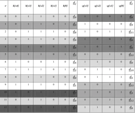
Table I. Wavelet coefficient (9/7) expressed in binary and showing common terms.
-r h[±4] h[±3] h[±2] h[±1] h[0]
𝑑𝑗
-g[±3] -g[±2] -g[±1] -g[0] 𝑑𝑗
0 0 1 1 0 0 𝑑0 1 0 0 1 𝑑6
1 0 1 1 0 1 𝑑3 1 0 0 0 𝑑9
2 0 1 1 1 0 𝑑8 1 0 1 1 𝑑11
3 0 1 1 0 0 𝑑0 1 0 0 1 𝑑6
4 0 1 0 0 1 𝑑6 1 0 0 1 𝑑6
5 0 1 1 0 1 𝑑3 0 0 1 0 𝑑12
6 1 0 0 1 0 𝑑4 1 1 0 0 𝑑0
7 1 1 1 0 1 𝑑2 0 1 1 0 𝑑10
8 0 1 1 0 0 𝑑0 0 1 1 1 𝑑5
9 1 1 1 0 0 𝑑1 0 0 1 0 𝑑12
10 1 0 1 1 1 𝑑7 1 1 0 1 𝑑3
11 0 1 1 0 0 𝑑0 0 0 1 0 𝑑12
ISSN: 2393-8366
646
For convenience we consider h[j] and –g[j] instead of h[j] an g[j] so as to find out more common terms and have common subexpression elimination. To make the coefficients compatible with open jpeg model, we choose the h[j] and g[j] taps as one bit for integer part and 12 bits for fractional part. Hence coefficients are rounded to 13 decimal places. From the table 1, it is clear that the coefficients are symmetric in nature. The repeated common terms are grey shaded in similar manner. To have filter symmetry, the column vectors are arranged as
𝐶𝜔= {𝑥[𝑖 + 𝜔] + 𝑥[𝑖 − 𝜔]𝜔 = 1,2,3,4𝑥[𝑖]𝜔 = 0 (1)
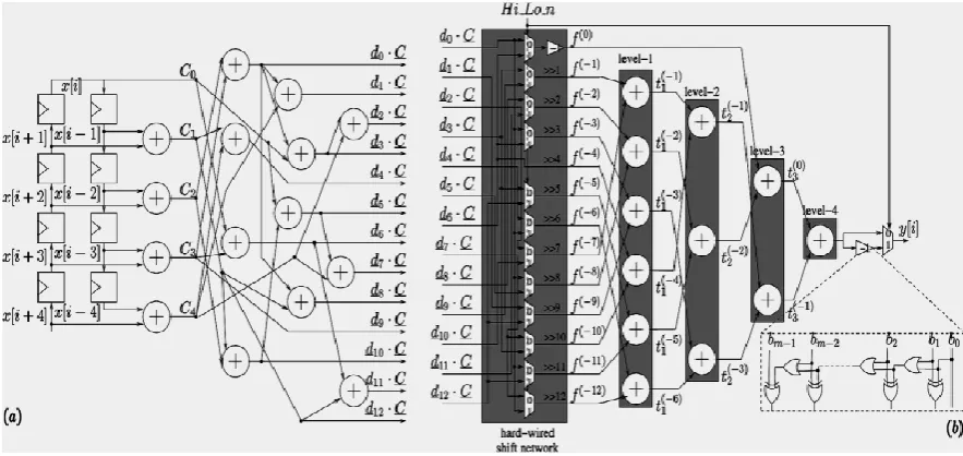
Where 𝑥[𝑖]is the i-th input applied 𝐶𝜔 is combined with 13 𝑑𝑗 values hence forming a butterfly
circuit as in figure 1(a). Inputs are given serially and stored in the register shifted at successive clock pulses. Thus the computations for the input say for example x[i-ω] and x[i+ω] (which should be actually computed six clock pulse hence) can be computed together. The adder used are normal ripple carry adders. Twenty seven adders, two negation block, fourteen 2:1 multiplexers and twelve shifting network, eight delay elements are employed. This causes the increased delay and power. Software building is made on Xilinx platform using verilog HDL coding.
The appropriate low pass and high pass filters are terms are selected using a Hi-Lo signal to the multiplexer. They are shifted and then added together at tree adder as shown in figure 1(b). For the 13 dj.c values, 13 shifts from 0 to 12 are applied (division) by the hardwired shifted network.
Figure 1. Butterfly circuit (a) and tree adder with hard-wired shift network computational scheme (b)
Moving on to the tree adder, the addition takes place in a fashion as below.
𝑡1(−𝑖) = 𝑓(−𝑖)+ 𝑓(−𝑛2−𝑖)
(2)
ISSN: 2393-8366
647
2. Spurious Power Suppression Technique
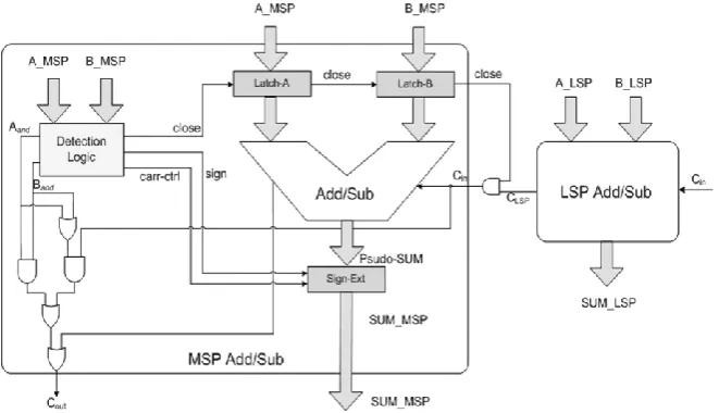
The result biased DA based DWT utilizes more than 25 adders for the implementation of 9/7 wavelet filter bank. The adder used here is ripple carry adder which utilizes more delay and power. With the help of spurious power suppression technique, these ripple carry adders are replaced using a low power adder. We aim to reduce about dynamic power consumption with a very little area augmentation. The proposed adder splits the input arriving to it into two parts. One least significant part (LSP) and other most significant part (MSP). Different cases have to be mentioned where the proposed adder is applicable. These special cases either have the MSB bits either as all ones or as all zeros. Whose value can be predetermined and can be avoided from calculating. The first case illustrates a transient state in which spurious transitions of carry signals occur in the MSP, although the final result of the MSP is unchanged. Meanwhile, the second and third cases describe situations involving one negative operand adding another positive operand without and with carry-in from the LSP, respectively. Moreover, the fourth and fifth cases demonstrate the addition of two negative operands without and with carry-in from the LSP, respectively. In those cases, the results of MSP are predictable; therefore, the computations in MSP are useless and can be neglected. Eliminating those spurious computations not only can save the power consumption inside the adder/subtractor in the current stage but also can decrease the glitching noises which cause power wastage inside the arithmetic circuits in the next stage. Fig. 2 shows a 16-bit adder/subtractor design example adopting the proposed SPST. In this example, the 16-bit adder/subtractor is divided into MSP and LSP between the eighth and the ninth bits.
Figure 2. Architecture of SPST adder.
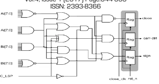
Latches implemented by simple AND gates are used to control the input data of the MSP. When the MSP is necessary, the input data of MSP remain unchanged. However, when the MSP is negligible, the input data of the MSP become zeros to avoid glitching power consumption. The two operands of the MSP enter the detection-logic unit, except the adder/subtractor, so that the detection-logic unit can decide whether to turn off the MSP or not. Based on the detection-logic unit of SPST is shown in Fig. 3 which can determine whether the input data of MSP should be latched or not.
ISSN: 2393-8366
648
Figure 3. Detection logic design
Fig. 3 shows the data-controlling components of the SPST, where Fig. 4 shows the design of the data latch. The inputs are loaded to the adder only when close signal is high else the inputs at adders are zeros and partial sum produced from adders are zeros and output is calculated from sign extension circuit.
Figure 4. Data latch design.
The SE circuits can be intuitively implemented by multiplexers to compensate for the sign signals of the MSP, as shown in Fig.5. The input data of the SE circuits are pseudo summations (PS) from the MSP adder/subtractors.
Figure 5. Sign extension unit design.
4. Conclusion
Discrete wavelet transform based image compression is very effectively trending nowadays. The project helps in bringing out an efficient way to reduce power consumption in the existing result biased distributed arithmetic based filter architectures for approximately computing DWT. The limitation is that we need to compromise the area occupied. The ripple carry adders in the above said paper are replaced using a spurious power suppression technique based adder expecting to reduce power dissipation. Exploring a comparative study on the paper is in advance. SPST technique is studied and researched. Base paper work is studied. Coding integration and comparison is progressing. As an advancement of the project more optimization of XOR gates can be done. This project has wide application in signal and image processing, biomedical applications including QRS peak detection signal denoising and image compression etc.
Acknowledgements
ISSN: 2393-8366
649
REFERENCES
[1] M. Boliek, JPEG 2000 Final Committee Draft 2000.
[2] A. Biligin and M. W. Marcellin, “JPEG2000 for digital cinema,” in Proc. IEEE Int. Conf. Circuits Syst., 2006.
[3] S. Mallat, “A theory for multiresolution signal decomposition: the wavelet representation,” IEEE Trans. Pattern Anal. Machine Intell, vol. 11, pp. 674-693, July 1989.
[4] M. D. Adams and F. Kossentini, “Reversible integer-to-integer wavelet transforms for image compression: performance evaluation and analysis,” IEEE Trans. On Image Processing, vol. 9, no. 6, Jun. 2000, pp. 1010-1024.
[5] C. T. Huang, P. C. Tseng, and L. G. Chen, “VLSI architecture for forward discrete wavelet transform based on B-spline factorization,” J. VLSI Signal Process., vol. 40, no. 3, pp. 343–353, Jul. 2005.
[6] M. Martina, G. Masera, and G. Piccinini, “Scalable low-complexity B-spline discrete wavelet transform architecture,” IET Circuits, Devices, Syst., vol. 4, no. 2, pp. 159–167, Feb. 2010.
[7] M. A. Islam and K. A. Wahid, “Area- and power-efficient design of Daubechies wavelet transforms using folded AIQ mapping,” IEEE Trans. Circuits Syst. II, Exp. Briefs, vol. 57, no. 9, pp. 716–720, Sep. 2010.
[8] S. K. Madishetty, A. Madanayake, R. J. Cintra, and V. S. Dimitrov, “Precise VLSI architecture for AI based 1-D/2-D Daub-6 wavelet filter banks with low adder-count,” IEEETrans.Circuits Syst. I, [9] S. Murugesan and D. B. H. Tay, “New techniques for rationalizing orthogonal and biorthogonal wavelet filter coefficients,” IEEE Trans. Circuits Syst. I, vol. 59, no. 3, Mar. 2012.
[10] A. Pande and J. Zambreno, “Poly-DWT: Polymorphic wavelet hardware support for dynamic image compression,” ACMTrans. Embedded Comput. Syst., vol. 11, no. 1, pp. 1–26, Mar. 2012. [11] A. K. Naik and R. S. Holambe, “Design of low-complexity high-performance wavelet filters for image analysis,” IEEE Trans. Image Process., vol. 22, no. 5, pp. 1848–1858, May 2013.
[12] S. Y. Park and P. K. Meher, “Low-power, high-throughput, low-area adaptive FIR filter based on distributed arithmetic,” IEEE Trans. Circuits Syst. II, Exp. Briefs, vol. 60, no. 6, 2013.
[13] M. S. Prakash and R. A. Shaik, “Low-area and high-throughput architecture for an adaptive filter using distributed arithmetic,” IEEE Trans. Circuits Syst. II, Exp. Briefs, vol. 60, no. 11, Nov. 2013.
[14] J. Xie, P. K. Meher, and J. He, “Hardware-efficient realization of prime-length DCT based Distributed arithmetic,” IEEE Trans. Comput., vol. 62, no. 6, pp. 1170–1178, Jun. 2013.
[15] Y. H. Chen, J. N. Chen, T. Y. Chang, and C. W. Lu, “High-throughput multistandard transform core supporting MPEG/H.264/VC-1 using common sharing distributed arithmetic,” IEEE Trans. Very Large Scale Integr. (VLSI) Syst., vol. 22, no. 3, pp. 463–474, Mar. 2014.
[16] M. Alam, C. Rahman, W. Badawy, and G. Jullien, “Efficient distributed arithmetic based DWT architecture for multimedia applications,” in Proc. IEEE Int.Workshop Syst.-on-Chip Real-Time Appl. Calgari, June 30–July 2 2003, pp. 333–336.
[17] X. Cao, Q. Xie, C. Peng, Q. Wang, and D. Yu, “An efficient VLSI implementation of distributed architecture for DWT,” in Proc. IEEE Workshop Multimedia Signal Process., 2006, pp. 364–367. [18] Maurizio Martina, Guido Masera, Massimo Ruo Roch, and Gianluca Piccinini, “Result-Biased Distributed-Arithmetic Based Filter Architectures for Approximately Computing the DWT”, IEEE Transactions On Circuits And Systems—I: Regular Papers, Vol. 62, No. 8, August 2015
ISSN: 2393-8366
650
ABOUT AUTHORS
Ms. Parvathy Mohan, currently pursuing PG in VLSI Design from IES College of engineering, Thrissur, Kerala, India. She received her Btech in Electronics and Instrumentation engineering from Cochin University of Science and Technology in the year 2009. Her interested research areas are VLSI Signal Processing, Electronic devices & circuits and Electronic Measurements & Instruments.
Ms. Bency Varghese A., currently working as Asst. Professor in department of Electronics and communication engineering with IES College of engineering, Thrissur, Kerala for the last 3 years. She graduated her Mtech degree in VLSI and Embedded systems from Cochin University of Science and Technology in the year 2013 and B.Tech degree in Electronics and Communication engineering from Calicut University in the year 2009. Her area of interest includes VLSI signal processing, Radio and Antenna propagation and embedded systems.