Effects of Mg Additions on Microstructure
and Optical Properties of Sol-Gel Derived ZnO Thin Films
Chien-Yie Tsay
1;*, Min-Chi Wang
1and Shin-Chuan Chiang
21
Department of Materials Science and Engineering, Feng Chia University, Taichung, Taiwan 40724, R.O.China 2Taiwan TFT LCD Association (TTLA), Hsinchu, Taiwan 31040, R.O.China
Polycrystalline thin-films of Zn1xMgxO (0x0:36) have been prepared by a sol-gel method and a spin-coating technique. In this
work, the authors investigate the effects of the Mg addition on crystallization, microstructure and optical properties for ZnO thin films. Mg was incorporated into ZnO thin films that were deposited onto glass substrates by a spin coating technique. The as-deposited films were preheated at 300C for 10 min and then annealed at 500C for 1 h. The results show that addition of Mg-species in ZnO films markedly decreased surface
roughness, improved transparency in the visible range and increased resistivity. Among the Zn1xMgxO films investigated in the present study,
the Zn0:8Mg0:2O thin film exhibited the best properties, namely single wurzite phase, an optical transmittance of 94.7%, an RMS roughness of
1.63 nm and a resistivity of8:3105-cm. [doi:10.2320/matertrans.MER2007334]
(Received December 21, 2007; Accepted February 26, 2008; Published April 16, 2008)
Keywords: ZnO, Zn1xMgxO thin films, optical properties, sol-gel method
1. Introduction
Wide bandgap (>3eV) transparent conductive oxides
(TCO), such as zinc oxide (ZnO), tin oxide (SnO2) and indium tin oxide (ITO), have been extensively used to make environmentally sustainable energy components and
optical-electrical systems.1)Among these materials, ZnO prepared at
low temperatures has properties including non-toxicity, high transparency, and high crystallinity. It has become a promising candidate for novel device applications, such as
transparent electronics2)and flexible displays.3)Owing to its
unique electrical and optical properties, it has been popularly used in varistors, chemical sensors, piezoelectric devices, etc. Recently, ZnO thin films have attracted interest for solar cell and flat panel display (FPD) applications, such as window
layers for thin film solar cells,4)transparent conductive layers
for touch panels5) and active channel layers for thin-film
transistors (TFTs).6)
ZnO is an n-type oxide semiconductor material with a direct wide bandgap of 3.35 eV. Its electrical characteristics can be controlled by doping or by incorporating ternary
elements,7,8) such as Al, In, Ga etc. The carrier mobility of
pure ZnO exceeds the field effect mobility of hydrogenated amorphous silicon (a-Si:H), which serves as an active channel layer material in typical TFT arrays. In addition, polycrystalline ZnO films can be prepared in a normal atmosphere. Because ZnO-based materials may replace amorphous silicon for active layer applications, this subject presently attracts much attention.
The solution-based process offers a simple and low cost thin film deposition method as an alternative to vacuum deposition techniques (PVD or CVD). Oxide semiconductor formed from the solution process may improve the manu-facturing throughput of microelectrical devices by enabling maskless processes, including inkjet printing and selective
electroless plating, etc.9) The sol-gel method is one of
common solution processes that is popularly used for
polycrystalline oxide thin film deposition.10,11) ZnO-based
semiconductor films have been shown to be suitable for
service as TFT active channel layers.12–15) Kwon et al.16)
indicated that to control the carrier density of the active layer in a ZnO-based TFT is a challenge, because the active layer supplies high carrier density that will be conducting when an
applied gate voltage is absent. The ionic radius of Mg2þ
(0.065 nm) is smaller than Zn2þ (0.074 nm), and thus the
solid solubility limit of MgO in ZnO can approach
40 at%.17,18)The incorporation of Mg into ZnO films tends
to decrease the interstitial oxygen vacancies19)and electron
density.20)Many reports have demonstrated that the solubility
limit of Mg content in Zn1xMgxO films strongly depends on
deposition or growth technique,e.g.PLD,18,21)sputtering,22)
MOVPE,17)and sol-gel method.23,24)
In the present study, polycrystalline Zn1xMgxO thin films
were fabricated by a sol-gel method and a spin coating technique; the effects of Mg additions on crystallinity, microstructure, and optical properties were investigated. Moreover, these thin films’ electrical characteristics were tested to determine whether these films could serve as TFTs active channel layers.
2. Experimental
To synthesize Zn1xMgxO sols, Mg2þ was varied from 0
to 0.36 (for x values); a mixture of zinc acetate dehydrate
(Zn(CH3COO)22H2O) and magnesium acetate tetra-hydrate
(Mg(CH3COO)24H2O) was dissolved in a solution of
2-methoxyethanol and monoethanolamine (MEA). The molar
ratio of MEA to metal ions in each Zn1xMgxO sol was
maintained at 1.0 and each concentration of metal ions was controlled at 0.75 mol/L. The complex solution was stirred
for 2 h at 60C until a clear, homogenous and stable sol was
obtained. All Zn1xMgxO gel films were coated onto
alkali-free glass (Corning 1737, with dimension 55cm2) using
spin coating at a speed of 3000 rpm for 30 seconds. The
as-*Corresponding author, E-mail: [email protected]
coated films were preheated at 300C for 10 mins
immedi-ately after coating. After repeating the coating procedure three times, the films were annealed in a tube furnace at
500C for 1 h in air.
After the annealing step, X-ray diffractometry (XRD, MAC Science MXP3, Japan) was used to examine the crystallinity levels of the pure ZnO and Mg incorporated ZnO thin films. The surface morphology and microstructure of
each Zn1xMgxO film were observed by scanning electron
microscopy (SEM, HITACHI S-4800, Japan). A scanning probe microscope (SPM, Digital Instrument NS4/D3100CL, Germany) was used to analyze the surface roughness levels of the films. The resistivities were measured by a high resistivity meter (MCP-HT450, DIA INSTRUMENTS CO., LTD, Japan). Moreover, optical transmittance spectra of these films were examined by a spectrophotometer (Mini-D2T, Ocean Optics Inc., USA).
In this study, Zn1xMgxO films served as the active
channel layers of TFTs. Figure 6(a) shows a schematic
diagram of a TFT with a Zn1xMgxO active layer. The
simple bottom-gate structure devices were fabricated by a hybrid method that combined the standard micro-electrical fabrication process and a solution-based process. Spin
coating finished each Zn1xMgxO TFT by depositing a
Zn1xMgxO thin film onto the multilayer MoW/SiO2/ITO
structure. The ID-VD characteristics of the transistors with
Zn1xMgxO active channel layers were measured in a dark
room using a semiconductor parameter analyzer (HP 4155B, USA).
3. Results and Discussion
Figure 1 presents XRD patterns of pure ZnO and Zn0:8Mg0:2O thin films. Two patterns correspond to three main diffraction peaks of the ZnO: (100), (002) and (101). All
Zn1xMgxO (x¼0{0:36) gel films were preheated at 300C
and then annealed at 500C, producing polycrystalline films
with hexagonal wurzite structure (Zincite, JCPDS 36-1451).
X-ray diffractographs of Zn1xMgxO films show that the
intensity of diffraction peaks decrease with increasing Mg content, viz. Mg incorporated within ZnO films caused the
crystallinity to degenerate. The Zn0:8Mg0:2O film shows a
highly c-axis oriented (002) peak (curve (b) in Fig. 1). To
estimate the average crystallite size (d) of these samples,
Scherrer’s formula25)is used;
d¼ 0:9 BcosB
; ð1Þ
whereis the X-ray wavelength of 0.154 nm,Bis the Bragg
diffraction angle and B is the FWHM (full width at half
maximum) ofB. The calculated average crystallite size of
Zn1xMgxO films are summarized in Table 1 that shows Mg
incorporated ZnO thin films have slightly reduced average grain size. The experimental results also show that when the Mg content is more than 30 at%, the MgO phase becomes segregated. In previous reports, the high solubility of Mg ions in ZnO films were demonstrated. For example, Ohtomo
et al.26)reported the soluble range of epitaxial Zn1xMgxO
films was from 0.25 to 0.33 in films that were grown by PLD.
Also, Zhaoet al.23)demonstrated that when the Mg content
exceeded 0.36, the MgO phase segregation would occur at
800C. In their study, the Zn1xMgxO films were fabricated
by sol-gel method.
After Mg incorporation, slight shifts are observed in the
(002) and (001) peaks. The lattice parameters of a- and
c-axes were calculated using a¼=pffiffiffi3sin and c¼
=sin, respectively. Figure 2(a) shows the two lattice
parameters as a function of Mg content. Results indicate that
Mg2þ substituted for Zn2þ can increase the a-axis length
from 0.3224 to 0.3240 nm and decrease c-axis length from
0.5195 to 0.5167 nm, when thex-value is below 0.3. It may
be the case that Mg substitution increases the strain in the
lattice.27)In films with up to33at% Mg incorporation, the
lattice parameters that changed were opposite to the parameters that changed in single-phase samples. Figure 2(b) shows Mg incorporated into ZnO thin films have slightly increased the cell volume.
25 35 45 55 65
(103)
(110)
(102)
(b)
(101)
(002)
Relative
intensity (arb.
unit)
2θ
(100)
(a)
Fig. 1 XRD patterns of (a) ZnO and (b) Zn0:8Mg0:2O thin films annealed at
[image:2.595.47.549.92.171.2]500C for 1 h.
Table 1 Average crystallite size, surface roughness, visible transmittance, optical bandgap and resistivity obtained for Zn1xMgxO thin
films.
xin Zn1xMgxO 0 0.1 0.2 0.3 0.33 0.36
Average crystallite size (nm) 8.9 8.8 8.7 8.4 8.5 8.4
RMS roughness (nm) 16.24 7.81 1.63 1.97 2.79 3.82
Transmittance(%) 83.5 91.1 94.7 93.1 93.4 88.5
Optical bandgap (eV) 3.24 3.36 3.51 3.52 3.47 3.47
Resistivity (-cm) 2:5103 2:7104 8:3105 6:4104 3:5104 2:5104
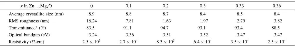
[image:2.595.312.541.199.387.2]Spin coating is a simple oxide thin film deposition technique, but it requires soluble types of reagents. It is possible to control the film thickness by merely adjusting the solution viscosity or coating times. The plane view of an SEM image of an annealed pure ZnO film shows fiber-like streaks or wrinkles (Fig. 3(a)). However, the incorporated samples do not display that appearance, as can be seen from
the surface image of Zn0:8Mg0:2O film (Fig. 3(c)). According
to a previous report,28)the fiber-like streaks or wrinkles are
induced by the shortness of OH and OR groups. Magnesium acetate tetrahydrate is a source for Mg ions, and thus can provide enough OH groups. Thus, a relatively smooth surface
can be obtained for Zn1xMgxO thin films. Cross-sectional
SEM images of the ZnO and Zn0:8Mg0:2O thin films are
shown in Figs. 3(b) and 3(d), respectively. Figure 3(b) is an SEM micrograph of the ZnO film that shows its average thickness is about 140 nm. Figure 3(d) shows that the average thickness of incorporated films is about 150 nm and addition of Mg-species to the ZnO films markedly improved the surface flatness and enhanced the uniformity of film thick-ness. This SEM image (Fig. 3(d)) also reveals that Mg incorporation in ZnO films can reduce the average crystallite size; XRD measurements confirm this finding.
When Mg incorporates with a ZnO thin film, it influences the surface morphology. It is apparent that Mg substitution in ZnO film causes a decrease in average crystallite size, which in turn causes a reduction of surface roughness. Table 1
presents the values of RMS roughness of Zn1xMgxO thin
films, and shows that Mg incorporation yields a significant improvement of surface roughness. Figure 4 shows the
0.0 0.1 0.2 0.3 0.4
140 141 142 143 144
ZnO+MgO
Mg content (x)
Cell v
olume
(
Å
)
ZnO (b)
0.0 0.1 0.2 0.3 0.4
3.20 3.22 3.24 3.26 3.28 3.30
ZnO
ZnO+MgO
Mg content (x)
a-axis length
(
Å
)
(a)
5.10 5.12 5.14 5.16 5.18 5.20
c-axis length (Å)
Fig. 2 (a) Thea- andc-axis lattice parameters and (b) the cell volume of Zn1xMgxO thin films as a function of Mg content.
(a)
1
µ
m
(b)
100nm
(d)
(c)
[image:3.595.57.280.70.400.2] [image:3.595.78.524.453.771.2]relationship of RMS roughness to Mg concentration; as Mg concentration increased from 0.0 to 0.2, RMS roughness decreased, but greater Mg concentrations increased
rough-ness. That is, among all of the annealed Zn1xMgxO thin
films in this study, the Zn0:8Mg0:2O thin film exhibited the
smallest RMS value, namely 1.63 nm.
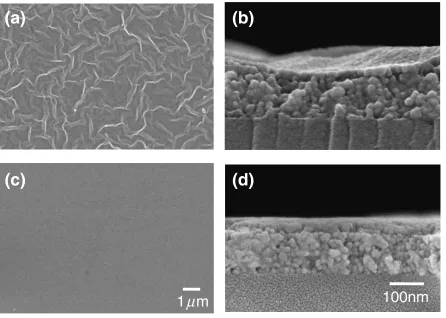
Figure 5(a) shows the optical transmittance spectra of the
Zn1xMgxO thin films examined at room temperature. All
samples showed sharp absorption edges in the UV region and these absorption edges shifted to shorter wavelengths when the ZnO thin films were augmented with Mg. A previous
study reported that the absorption maxima of Zn1xMgxO
films blueshifted as a function of the Mg content.13)For the
pure ZnO film, optical transmittance in the visible range was about 80% and the exhibited absorption edge approached 362 nm. Table 1 presents the transmittance levels at a wavelength of 550 nm; Mg incorporated samples show higher transparency levels than the pure ZnO sample. However, the transmittance was lower for higher Mg content
samples, with x0:3, than for the x¼0:2 sample. This
result is in good agreement with the results of XRD, SEM and SPM and relates to MgO phase segregation. In this study, the Zn0:8Mg0:2O sample exhibited 94.7% transparency, which was the best transparency among incorporated samples and gave an increase of about 13.5% over the pure ZnO sample. In direct bandgap semiconductors, the absorption edge
can be analyzed by the relation;29)
ðhÞ ¼AðhEgÞ1=2; ð2Þ
where is the absorption coefficient, h is the photon
energy, A is a constant and Eg is the optical bandgap. The
absorption coefficient () in the UV region of these
Zn1xMgxO thin films can be calculated fromI¼Ioet,30)
whereIis intensity of the transmitted light,Iois the intensity
of incident light and t is the thickness of the Zn1xMgxO
films. Figure 5(b) is the plot of ðhÞ2 vs. photon energy.
These curves are evaluated from the transmittance spectra in Fig. 5(a). Extrapolation methods can determine the optical
bandgaps of Zn1xMgxO thin films. The optical bandgap
values (Eg) listed in Table 1 show the bandgap increased
with Mg content, from 3.24 eV to 3.52 eV, for0x0:3.
Cohenet al.20)have indicated thatE
gvalues of Zn1xMgxO
increases further to 3.64 eV due to the Burstein-Moss
shift.31) In films with x values exceeding 0.3 the Eg
approaches 3.47 eV. It is possible that second phase segregation caused this effect.
ZnO exhibits wide-range conductivity; its behavior ranges from metallic to insulating. Its electrical characteristics can be controlled by doping with ternary elements or adjusted process conditions. Table 1 shows the resistivity values
of Zn1xMgxO thin films with various Mg content. The
resistivities of ZnO films increased one or two orders of
magnitude when Mg was incorporated and the Zn0:8Mg0:2O
sample exhibited the highest resistivity among incorporated
samples, 8:3105-cm. Liu et al.32) have reported that
when Mg is doped into ZnO, interstitial metal atom and oxygen vacancies can be depressed. A Mg-doped ZnO film’s appearance increases its resistivity.
An MgO formation as a secondary phase above the
solubility limit of Zn1xMgxO phase can cause degeneration
of crystallinity, electrical and optical properties. The present
research suggests that, in order to make sure the Zn1xMgxO
film possesses pure hexagonal crystal structure, the Mg2þ
content should not be greater than x¼0:3. A single-phase,
defect-free polycrystalline semiconductor thin film with uniform thickness and a flat surface can serve as an active channel layer for carrier propagation from source to drain
0.0 0.1 0.2 0.3 0.4
0 5 10 15 20
RMS
roughness (nm)
Mg content (x)
Fig. 4 Surface roughness of Zn1xMgxO thin films as a function of Mg
content.
200 400 600 800 1000
0 20 40 60 80 100
x=0 x=0.1 x=0.2 x=0.3 x=0.36
T
ransmittance (%)
Wavelength (nm)
(a)
3.0 3.2 3.4 3.6 3.8 4.0
(
α
h
υ
)
2 (a.u.)
Photon energy, hυ (eV)
x=0 x=0.1 x=0.2 x=0.3 x=0.36
(b)
Fig. 5 (a) Optical transmittance spectra and (b) plot ofðhÞ2vs. photon
[image:4.595.57.284.70.246.2] [image:4.595.56.284.298.653.2](Fig. 6(a)). Figure 6(b) shows a local cross-section view of a
Zn0:8Mg0:2O TFT. The image shows that the Zn0:8Mg0:2O,
film was successfully deposited on a multilayer device and did not cause defects on interfaces between ITO/ Zn0:8Mg0:2O or SiO2/Zn0:8Mg0:2O.
Figure 7 shows the drain current-drain voltage (ID-VD)
characteristics of Zn1xMgxO TFTs. It shows that these field
effect transistors operated in an n-type enhancement mode and the drain current increases with positive gate bias.
Further, the slope of eachIDcurve is flat and exhibits a hard
saturation for large VD region. Hoffaman et al.33) have
indicated that hard saturation can deplete the entire layer of
the ZnO-based active channel of free electrons and that large output impedance is desirable for most circuit applications. The field-effect mobility of TFT devices depend on the
saturated current. Therefore, the Zn0:8Mg0:2O TFTs exhibit
the best performance among our samples, according toID-VD
characteristics.
4. Conclusions
Magnesium substituted zinc oxide thin films have been prepared successfully by solution-based process that com-bined a sol-gel method and a spin-coating technique. The heat-treated films that have less than 0.3 Mg addition exhibits
wurzite phase; those films with higher Mg levels (x0:3)
show segregation of MgO and degrade film quality. The additions of Mg into ZnO thin films not only refine the grain size but also increase the transmittance of thin films. Among
the Zn1xMgxO (0x0:36) films investigated in the
present study, the Zn0:8Mg0:2O film exhibits the best
trans-parency and the highest resistivity. Its average crystallite size is 8.7 nm with its transparency and resistivity of 94.7%
and8:3105-cm, respectively.
Acknowledgments
The authors gratefully acknowledge the financial support by the National Science Council of Republic of China under Contract No. NSC 95-2221-E-035-006 and Taiwan TFT-LCD Association (TTLA) under Contract No. A643TT1000-S11.
REFERENCES
1) H. Ohta and H. Hosono: Materials Today7(2004) 42–51. 2) J. F. Wager: Science.300(2003) 1245–1246.
3) A. N. Banerjee, C. K. Ghosh, K. K. Chattopadhyay, H. Minoura, A. K. Sarkar, A. Akiba, A. Kamiya and T. Endo: Thin Solid Films.496 (2006) 112–116.
4) W. Li, Y. Sun, Y. Wang, H. Cai, F. Liu and Q. He: Solar Energy Mater. Solar Cells.91(2007) 659–663.
5) B. Y. Oh, M. C. Jeong and J. M. Myoung: Appl. Surf. Sci.253(2007) 7157–7161.
6) R. B. M. Cross and M. M. De Souza: Appl. Phys. Lett.89(2006) 263513.
7) D. P. Norton, Y. W. Heo, M. P. Ivill, K. Ip, S. J. Pearton, M. F. Chisholm and T. Steiner: Materials Today7(2004) 34–40.
8) F. Oba, T. Yamamoto, Y. Ikuhara, I. Tanaka and H. Adachi: Mater. Trans.43(2002) 1439–1443.
9) T. W. Fang, S. C. Chiang, B. C. Chuang, C. H. Tsai, C. Y. Huang, C. C. Hsu, W. C. Lin, S. H. Lai and S. Y. Meng: Proceedings of International Display Manufacturing Conference (IDMC’07). (2007) pp. 585–587. 10) T. Hashimoto and T. Yoko: Mater. Trans. JIM37(1996) 435–441. 11) L. Shen, D. Xiao, P. Yu, J. Zhu, D. Gao, G. Yu and W. Zhang: Mater.
Trans.44(2003) 1324–1327.
12) B. J. Norris, J. Anderson, J. F. Wager and D. A. Keszler: J. Phys. D: Appl. Phys.36(2003) L105–L107.
13) E. Fortunato, P. Barquinha, A. Pimentel, A. Goncalves, A. Marques, L. Pereira and R. Martins: Thin Solid Films.487(2005) 205–211. 14) J. H. Lee, P. Lin, C. C. Lee, J. C. Ho and Y. W. Wang: Jpn. J. Appl.
Phys.44(2005) 4784–4789.
15) Y. J. Chang, D. H. Lee, G. S. Herman and C. H. Chang: Electrochem. Solid-State Lett.10(2007) H135–H138.
16) Y. Kwon, Y. Li, Y. W. Heo, M. Jones, P. H. Hollyway, D. P. Norton, Z. V. Park and S. Li: Appl. Phys. Lett.84(2004) 2685–2687. 17) W. I. Park, G. C. Yi and H. M. Jang: Appl. Phys. Lett.79(2001)
0 20 40 60 80 100
0 5.0x10⁻⁶ 1.0x10⁻⁵ 1.5x10⁻⁵ 2.0x10⁻⁵
2.5x10⁻⁵ Gate voltage=100V
x=0.1 x=0.2
Drain current,
ID
(A)
Drain voltage, VD (V) x=0
Fig. 7 ID-VDcurves of Zn1xMgxO TFTs with various Mg content.
MoW
SiO
2Zn
0.8Mg
0.2O
ITO
100 nm
(b) (a)
2)
Substrate (Alkali-free glass) Gate (MoW)
Source (ITO) Drain (ITO) Active channel layer
Gate insulator (SiO
Fig. 6 (a) Schematic diagram of Zn1xMgxO TFT and (b) local
[image:5.595.52.287.75.366.2] [image:5.595.56.281.423.597.2]2022–2024.
18) J. W. Kim, H. S. Kang, J. H. Kim, S. Y. Lee, J. K. Lee and M. Nastasi: J. Appl. Phys.100(2006) 033701.
19) Y. Ogawa and S. Fujihara: Phys. Stat. Sol. (a).202(2005) 1825–1828. 20) D. J. Cohen, K. C. Ruthe and S. A. Barnett: J. Appl. Phys.96(2004)
459–467.
21) T. Maemoto, N. Ichiba, S. Sasa and M. Inoue: Thin Solid Films.486 (2005) 174–177.
22) Dhananjay and S. B. Krupanidhi: Appl. Phys. Lett.89(2006) 082905. 23) D. Zhao, Y. Liu, D. Shen, Y. Lu, J. Zhang and X. Fan: J. Crystal
Growth.234(2002) 427–430.
24) C. S. Suchand Sandeep, R. Philip, R. Satheeshkumar and V. Kumar: Appl. Phys. Lett.89(2006) 063102.
25) B. D. Cullity and S. R. Stock:Elements of X-ray Diffraction, (Prentice-Hall, Inc, New Jersey, 2001) pp. 388.
26) A. Ohtomo, M. Kawasaki, T. Koida, K. Masubuchi, H. Koinuma, Y. Sakurai, Y. Yoshida, T. Yasuda and Y. Segawa: Appl. Phys. Lett.72 (1998) 2466–2468.
27) M. Ghosh and A. K. Raychaudhuri: J. Appl. Phys.100(2006) 034315. 28) G. W. Scherer: J. Sol-Gel Sci. Tech.8(1997) 353–363.
29) K. H. Kim, K. C. Park and D. Y. Ma: J. Appl. Phys. 81 (1997) 7764–7772.
30) R. D. Tarey and T. A. Raju: Thin Solid Films.128(1985) 181–189. 31) A. Sarkar, S. Ghosh, S. Chaudhuri and A. K. Pal: Thin Solid Films.204
(1991) 255–264.
32) J. Liu, W. Weng, W. Ding, K. Cheng, P. Du, G. Shen and G. Kan: Surf. Coat. Technol.198(2005) 274–277.