Abstract— This paper exemplifies one practical way to design high speed symbol timing recovery using the parallel architecture to cope with time constraint of computational processing. Recently, as wideband satellite transponders that have 200 to 300MHz come out and active study is followed for efficient transmission in terms of power/bandwidth based on single carrier transmission. When taking into account a single carrier transmission, receiver for instance should be able to work at maximum 250MHz symbol rate on 300MHz transponder bandwidth. However, straightforward parallel processing entails increased amount of computational logic and makes it difficult for massive ASIC chipset production. As a result, this paper specifies efficient parallel processing of blocks susceptible to processing latency and manifests its effectiveness by means of performance assessment and FPGA implementation.
Index Terms— Satellite, Wideband transponder, High speed symbol timing recovery, Parallel processing
I. INTRODUCTION
ECENTLY efficient utilization of wideband satellite transponder like Ka band for satellite broadcasting and interactive service is noticeable. Specifically, DVB (Digital Video Broadcasting)-S2(Satellite, Second generation) standard releases a salient way to perform it like time-slice transmission. [1] Meanwhile, Ku band transponder identified as 36MHz typically accommodates a single modulated carrier signal that can make use of the entire bandwidth because its transceiver has been widespread. If it’s applied to Ka band, most of transponder bandwidth used should be split into multiple carriers so that Ku transceiver can directly be used. The use of a single carrier per transponder is desirable in terms of power efficiency which enables TWTA(Traveling Wave Tube Amplifiers) to operate close to saturated output power range. Furthermore, it doesn’t necessitate extra guard band compared with multiple ones to avoid impairment like intermodulation distortion. Therefore, necessity of Ka band transceiver may arise. In addition, this technical benefit, the new promising service suited for Ka band like UHDTV(Ultra High Definition TeleVision) that requires much higher data rate, stimulates to develop Ka band transceiver that can cover wideband transponder. Consequently, it may envisage new approach to ensure transmission efficiency and flexibility through application of single wideband carrier. To realize Ka band transceiver, the
Manuscript received July 23, 2013; revised Aug 20, 2013.
Pansoo Kim and Deock-Gil Oh are with the Electronics and Telecommunication Research Institute, Deajeon, Republic of Korea 305-350 (e-mail: pskim@ etri.re.kr, [email protected]).
most critical component is designated to LDPC(Low Density Parity Check) decoder in the DVB-S2 standard because the number of memory size leads to increase due to parallel bit-to-check node processing as high data throughput augments.[1]
For state of the art DVB-S2 standard, time slice protocol was illustrated to send desire signal carried with Time Slice Number. Its receiver can select only wanted signals through its identification process. It seems to be appropriate because multimedia stream data have been carried as TDM(Time Division Multiplexing) in the satellite link. Moreover, the receiver may be able to deal with incoming data without high speed processing capability with proportional to transmission data rate because unwanted signal can be discarded.
When one scrutinizes the demodulator, initial acquisition blocks at least do work with closely single wide bandwidth rate, after called as full speed to handle with continuous stream efficiently and others can process as desired signal rate which is dependent of LDPC decoder capability. For specific blocks mentioned, ADC(Analog Digital Convertor), AGC(Automatic Level Control), MF(Matched Filter) and STR(Symbol Timing Recovery) ones may be desirable to run at full speed. This paper focuses on clock recovery because it appears to be some timing critical path among component block at higher full speed operation. The rest of the paper is organized as follows. In the Section II, we review the conventional digital timing recovery schemes for high speed processing. The Section III illustrates the proposed parallel timing recovery architecture. The simulation and implementation results are reported in the Section IV. The Section V draws the conclusion.
II. OVERVIEW OF STRSCHEME A. Signal Model
STR algorithm for TDM stream reception has been studied consistently. It can typically classify two different approaches. First one characterizes feedback loop.[2-10] The other does feedforward estimation and compensation.[11] The former can be simply implemented but need large initial acquisition time depending on loop parameters and channel condition. On the other hand, the latter can accomplish rapid timing synchronization but it’s rather sensitive to design parameters like window length according to carrier freq. offset. Moreover, a scheme using four samples per symbol is widely used for reliable performance. Accordingly, feedback approach is frequently used for satellite broadcasting and communication protocol as type of continuous stream TDM like DVB-S2 standard. The received signal r(t) in the baseband can be written as
Study of Clock Synchronization for High Speed
Satellite Communication Transmission
Pansoo Kim and Deock-Gil Oh
( ) ( ) ( ) ( ) k
r t s t g t kT n t ¥
=-¥
=
å
- + (1) where T symbol period, s t( )k-th transmitted complex multi-level signal, g(t) channel impulse response like ISI(Inter Symbol Interference), and n(t) complex AWGN(Additive White Gaussian Noise) signal. The perfect carrier recovery is assumed to be done for simplicity. (Normal mode): The sampling rate of Rx(receiver) is exactly double over symbol rate of Tx(Transmitter). This is the ideal situation when there is only a constant sampling time phase offset between Tx and Rx sampling clock. In this case, it stands for normal mode. The samples are fed into delay line as FIFO(First Input First Output) of interpolator and then interpolation filter works to find proper interpolant(a point interpolated between others) value computed by fractional delay µ on time through recursive loop process. The fractional delay can be defined as resampling point computed from multiple samples.(Skip mode): The sampling rate of Rx is slightly higher than two of symbol rate in Tx. In this case, it has more incoming samples at FIFO in Rx than going out. It denotes “skip mode” and can illustrate input(master clock) and output clock rate have no accurate consistency. The sampled signals are fed into FIFO but interpolation filter is frozen to compute interpolant value by TEC(Timing Error Controller) in NCO (Numerical Controlled Oscillator) block.
(Stuff mode): The sampling rate of Rx is slightly less than two of symbol rate in Tx. In that case, it has less samples incoming at STR block than going out. It denotes “Stuff mode”. No new sample is fed into FIFO but interpolation filter is worked. This case usually comes from normal mode, once µ is updated to a negative value less than zero. In such a case, time duration of one input sample may lead to two output samples at the output block of interpolation filter.
B. The Concept of Skipping Mode
This subsection explains sampling offset model, analytically. In general, ADC clock has at least more than two times sampling rate than symbol rate in terms of some practical reasons. In this case, skip mode has been frequently occurred. Specifically, input sample rate is 2(1+e)R andTs=T/ 2(1+e) where R symbol rate,
e
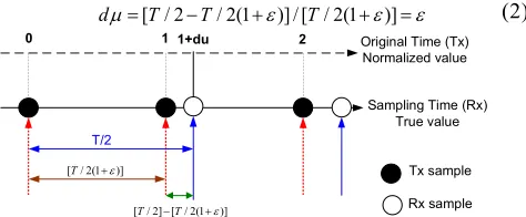
the amount of gap between transmitter and receiver clock rate(very small positive rational number less than one) and Ts sampling time interval. Let each sample interval correspond to an integer value from interpolator formula.[3] According to theTs<T/ 2Nyquist rule, if interpolant can be computed by µ at time t=nTs ,then it can be obtained by µ+dµ at time t=(n+1)Ts where dµ is the incremental variation amount of sampling clock offset regularly, after called sampling time drift in the Eq.(2) and Fig. 1.dm=[ / 2T -T/ 2(1+e)] / [ / 2(1T +e)]=e (2)
Sampling Time (Rx) True value Original Time (Tx) Normalized value
T/2
0 1 1+du 2
[ / 2(1T +e)]
[ / 2] [ / 2(1T -T +e)]
[image:2.595.52.289.672.770.2]Tx sample Rx sample
Fig 1. Conceptual diagram for skip mode
C. The Previous Study for High Speed STR Processing It has been extensive study for STR scheme literarily but it's not widely known for high speed processing dedicated. The references,[6][7] suggest the scheme that is capable of parallel processing with sampling dropping unit. However, there are no specific description for the other units such as specific interpolator architecture, TED, loop filter and NCO design for high speed processing. The references [8-10], select the different TED[11] called O&M(Oerder & Meyr) unlike this paper and provide specific implementation results. They use IDFT(Inverse Discrete Fourier Transform) computation based on four times samples per symbol. The interpolator control unit is characterized to work as type of LUT(Look Up Table) for high speed processing instead of programmable FIR filter proposed in this paper. According to computational analysis, it inevitably yields somewhat large complexity and introduction of higher speed ADC chips due to four samples per symbol even if accurate estimate is achievable. The reference [9][10] illustrates the detail information that it employs four parallel paths without increasing clock speed due to the limit of maximum operational speed, 188MHz and as a result, comes to increases complexity. In the meantime, the simplest way like M&M(Muller and Muller)[12] using one sample per symbol can be imaginable for high speed processing but it's known as much susceptibility over large carrier frequency offset and pattern jitter incurred by multi-level signal like 16APSK(Amplitude Phase Shift Keying) and 32APSK. In addition, it’s not suited to co-operate with interpolation filter. The Gardner TED used in this paper has been introduced in a lot of literatures due to robust characteristic but it's been so far never provided over parallel processing architecture. The main contribution of this paper is to propose the new architecture to increase operational speed and to compare with previous design in terms of performance and complexity
III. THE PROPOSED ARCHITECTURE
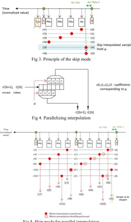
The section III addresses entire architecture for parallel processing of STR block underlined in this paper like Fig. 3. Based on the assumption like Eq.(2), ADC clock rate is slightly higher than the rate of two samples per symbol. From MF output signal, a series of input samples are divided into one to two de-multiplexer and it means the clock rate can be reduced to half. Here, we denote the divided samples as precedent r(2kTs)and current r((2k+1) )Ts where k is integer number. Accordingly, the main operational clock rate becomes symbol rate as a half of sampling rate thanks to parallel path. Based on this formula, as the number of parallel processing blocks increases, as higher symbol rate processing also can be achieved like[8-10], straightforwardly. However, it can have high complexity and requires careful design of the unit of interpolator and SEM(Skip Engine Machine) modification caused by amount of sampling clock offset and the number of sampling. It’s not affordable to extend much partial parallelism related with operational principle. The detail description is following.
A. Processing Unit
NCO. To reduce the complexity, MF and interpolator could be integrated but it should be optimized toward one of the two because characteristic of two FIR(Finite Impulse Response) filters are different. Although MF is involved in processing input signal at close to full speed, it can undertake rather comfortably in terms of computational time because polyphase FIR filter processing can be allowed by constant coefficient. When µ≥1, then one sample is skipped to maintain the range of µ in [0,1) as shown like Fig. 3. Note that when the sample s5 over background in Fig. 3 goes into the delay line FIFO of interpolator, the sample of interpolator output is skipped and the fractional delay µ is kept unchanged like normal mode. In addition, the sampling time drift dµ is continuously added to µ like Fig. 2. Taking into account the condition where the drift dµ is smaller than zero, the identical value of µ can be used twice for successive interpolators. This case happens when two complex samples per clock cycle(symbol clock) are fed into delay line of interpolator shown like Fig. 4 and Fig. 5. When we deal with two complex samples as parallel processing to reduce the operational clock speed in interpolator block, we notice that time drift is not dµ but 2dµ any longer because a couple of samples enter the interpolator like Fig. 4. Additionally, the sample to be skipped is always an even index like r(8) of green dot line in Fig. 5. The impulse response of interpolator can be derived as
2
2
2
2
(0) ( )
(1) ( ) 1
(2) ( )
(3) ( )
IR IR IR IR
a m m
a m m m
a m m m
a m m
=
-= - - - +
= - - +
=
-(3) where a=0.5. Let B(.) be interpolator complex FIFO as delay line, interpolator complex output can be expressed like Eq.(4)
(3) (0) (2) (1) (1) (2) (0) (3) I
z =IR B +IR B +IR B +IR B (4) where zI interpolator output signals. Eq.(5) can be induced from eq.(3) and (4)
2
( )[ (0) (1) (2) (3)] I
z =a m -m B -B -B +B [ (2)B B(3)] B(3) m
+ - + (5)
2(1+e)Rs
(1+e)Rs
(2 s) r kT
((2 1) )s
r k+T
(2 s) r kT
((2 1) )s
r k+T
2 p
m
[image:3.595.304.566.51.495.2](1+e)Rs (1+e)Rs
Fig 2. Detail description of STR unit
Fig 3. Principle of the skip mode
Fig 4. Parallelizing interpolation
Fig 5. Skip mode for parallel interpolation
Let us define Dij=B i( )-B j( ) and Dijkl =Dij - Dkl, then it
can be drawn to Eq.(6)
1234 (0) (1) (2) (3)
D =B -B -B +B
23 (2) (3)
[image:3.595.48.264.532.697.2]Fig 6. Pipeline structure for interpolator
B. Error Control Unit
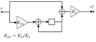
The ECU(Error Control Unit) in Fig. 3 consists of Gardner TED, loop filter and NCO blocks. The TED and loop filter based on PLL(Phase Locked Loop) become active only when the SEM block signals that outenable (output symbol is effective) signal is valid in Fig. 2. Otherwise, PLL filter output, p2 that denotes the loop filter output signal, becomes
zero to hold NCO control. The NCO block is to generate µ and to generate skip control signal. These two signals are updated at every clock cycle. The ECU is activated only when interpolator output samples are valid at the process unit output. The Gardner [2][5] algorithm for TED is selected that is widely known to work at two samples per symbol. Let
n n n
z =x + jy the n-th complex input sample at 2Rs at the TED input. Assuming that on time samples are indexed with even number, timing error is calculated as
*
2 1 2 2 2
Re{ ( )}
G
n n n n
e = z + z + -z
=x2n+1(x2n+2-x2n)+y2n+1(y2n+2-y2n) (7)
The loop filter is a proportional and integral filter. Its z-transfer function can be shown in 1
1 2
( ) /
F z K K z
-= + . Due
to the difference between K1 and K2 as loop filter coefficient, the dynamic can be handled with the following equivalent structure easily. Loop parameters K1 and K2 can be related to TED gain Gd 0.5, the loop noise bandwidth B TL 0.0005 and the damping factor x set to 1/ 2 as follows
2
8 / (1 4 )
o L
w = xB T + x (8)
2 2
2 (1 / d) o / (1 3 o )
K = G ´w + xw +x (9)
1 2 (1 2 / o)
K =K ´ + x w (10)
1 21 2/ 1 (1 2 / o)
K K K x w
-= = + (11)
[image:4.595.346.511.58.131.2]
Fig 7. Implementation of the Gardner TED
Fig 8. Loop filter structure
The most significant bit of NCO output can control skip mode. When a skip mode is detected, the increment should be p2+dµ
instead of p2+2dµ like Eq.(12). The NCO accumulates time
increments
( ) ( ( ) 1) skip n =
å
n ³( ) ( ) 0
( )
( ) 1 ( ) 1
n if skip n n
n if skip n
m = íìï =
- =
ï î
å
å
(12)where,
å
(n+1)= f n( )+m( )n2
2
[2 ( )] ( ) 0
( 1)
[ ( )] ( ) 1
d p n if skip n f n
d p n if skip n m
m
+
+
+ =
ì + = í
+ =
î
IV. IMPLEMENTATION AND RESULT
The proposed algorithm is designed and implemented as reported in the section III and obtains the results of timing jitter and PER(Packet Error Rate) performance in tracking mode and complexity assessment. The performance of the suggested architecture is measured at the COTS H/W board developed by ETRI after FPGA(Field Programmable Gate Array) configuration. For high speed ADC, the AD9434 model produced from the Analog Device©, is used to generate 12 bits sampling signal as input of MF. The result of maximum operational clock rate comes to 250MHz in case of selecting FPGA Xilinx XC6vlx550t model. For quantized process to be high speed operation the baseband complex signal is expressed by 8 bits (including signed bit) and all quantized bits of signals are present over Fig. 2 as red color over signal path. For entire design blocks, consecutive multiplication process in interpolation block is found as the most critical path in terms of timing latency. Therefore, it implies that we can achieve more increase of operational clock speed through the elaborated pipeline design. On the other hand, all optimum parameters like the loop bandwidth so that STR can track properly by maximum 10ppm clock drift error over the accurate sampling clock are selected in section III.(b). This paper shows the comparable results according to the algorithms using different oversamples (two and four) per symbol like [8-11]. The PER performance clarifies the benefit from double sampling signals is negligible as less 0.1dB gain in Fig. 9 through one MODCOD(Modulation and Coding Rate) selection of DVB-S2 standard. The metric of timing jitter performance when STR is in steady state mode can be defined as
2 2
[ ] [ ]
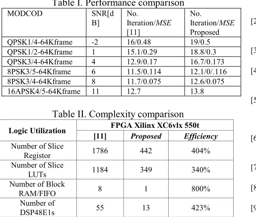
[image:4.595.72.260.439.709.2]Table I. Performance comparison
MODCOD SNR[d
B]
No. Iteration/MSE
[11]
No. Iteration/MSE
Proposed QPSK1/4-64Kframe -2 16/0.48 19/0.5 QPSK1/2-64Kframe 1 15.1/0.29 18.8/0.3 QPSK3/4-64Kframe 4 12.9/0.17 16.7/0.173 8PSK3/5-64Kframe 6 11.5/0.114 12.1/0/.116 8PSK3/4-64Kframe 8 11.7/0.075 12.6/0.075 16APSK4/5-64Kframe 11 12.7 13.8
Table II. Complexity comparison
Logic Utilization FPGA Xilinx XC6vlx 550t [11] Proposed Efficiency
Number of Slice
Registor 1786 442 404%
Number of Slice
LUTs 1184 349 340%
Number of Block
RAM/FIFO 8 1 800%
Number of
DSP48E1s 55 13 423%
For H/W complexity comparison, this paper seeks to build fair comparison condition due to the different system scenario. The efficiency of H/W utilization can be interpreted at two points of view. First, the fact is obvious that Gardner algorithm based on two oversampling must be simple compared to four oversampling and frequency domain processing of O&M algorithm [8-11]. Second, the architecture can be efficient in terms of the computational amount because this can reduce the number of parallel path by maximizing operational clock speed through some pipeline method like interpolator compared to the reference [8-10].
V. CONCLUSION
[image:5.595.51.272.553.712.2]In this paper, we investigate low complexity STR architecture with parallel processing to support high symbol rate. The proposed one is validated through performance evaluation and complexity comparison through FPGA implementation The result of FPGA synthesis and P&R(Place & Routing) as ISE software produced by Xilinx reports to have maximum operational speed by 250MHz. As a result, we can demonstrate that it’s applicable for efficient single carrier transmission on 300MHz transponder allowing for some small excess bandwidth.
Fig 9. PER performance comparison
REFERENCES
[1] DVB BlueBook A83 (2012-07) "Digital Video boradcasting(DVB); Second Generation Framing Structure, Channel Coding and
Modulation Systems for Broadcasting, Interactive Services, News Gathering and other broadband satellite applications".
[2] F.M. Gandner, "A BPSK/QPSK timing-error detector for sampled receivers," IEEE Trans Commun. vol. COM-34, pp.423-429, May. 1986.
[3] F.M. Gandner, "Interpolation in digital modems-Part I: Fundamentals," IEEE Trans. Commun., vol. 41, no. 3, pp.501-507, Mar. 1993. [4] L. Erup, F. M. Gardner and R. A. Harris, "Interpolation in digital
modems-part II: Implmentation and performance," IEEE Trans. Commuin. vol. 41, no. 6, pp.998-1008, Jun. 1993.
[5] E. Casini, R. De Gaudenzi, A. Ginesi: "DVB-S2 modem algorithms design and performance over typical satellite channels", International Journal on Satellite Communication Networks, vol.22, no.3,pp.281-318, May 2004.
[6] D. Schmidt and B. Lankl, "Parallel architecture of an all digital timing recovery scheme for high speed receivers," Proc. of CSDSP2010, pp.31-34, Jul. 2010.
[7] D. Schmidt and B. Lankl, "Structure of a Digital Feedback Clock Recovery for Parallelized Receivers" Proc. of SPPcom2011, Jun. 2011. [8] C. Lin, B. Shao and J. Zhang, "A high data rate parallel demodulator
suited to FPGA implementation," Proc. of ISPACS2010, Dec. 2010. [9] C. Lin, B. Shao and J. Zhang, "A High Speed Parallel Timing Recovery
Algorithm and Its FPGA Implementation," Proc. of IPTC2011, pp.63-66, Oct. 2011.
[10] C. Lin, J. Zhang and B. Shao, “A Multi-Gigabit Parallel Demodulator and Its FPGA Implementation,” IEICE Trans. Fundamentals. vol.E95-A No.8 pp.1412-1415, Aug. 2012.
[11] M. Oerder and H. Meyr, "Digital filter and square timing recovery," IEEE Trans. Commun. vol. 36, no. 5, pp.605-612, May 1988. [12] K. H, Muller and M. Muller, "Timing recovery in digital synchronous
data receeivers," IEEE Trans. on Commun. vol. com-24, no. 5, pp. 516-531, May 1976.