INTERNAL DOCUMENT 1 6 1
INTERFACE BETWEEN A MICROCOMPUTER AND THE ELECTRONIC MODEL FOR TIDES AND STORM SURGES
S. Ishiguro &
Kathleen Reeves-Wilkin 1982
[This document should not be cited in a published bibliography, and is supplied for the use of the recipient only].
INSTITUTE OF OCEANOGRAPHIC SCIENCES
Wormley, Godalming, Surrey GU8 5UB
(042-879-4141)
(Director; Dr. A . S. Laughton, FRS)
Bidston Observatory,
Birkenhead,
Merseyside L43 7RA
(051-653-8633)
(Assistant Director: Dr. D. E. Cartwright)
Crossway,
Taunton,
Somerset TA1 2DW
(0823-86211)
INSTITUTE OF OCEANOGRAPHIC SCIENCES INTERNAL DOCUMENT 161
INTERFACE BETWEEN A MICROCOMPUTER AND THE ELECTRONIC MODEL FOR TIDES AND STORM SURGES
S. Ishiguro &
Kathleen Reeves-Wilkin 1982
1. Introduction 2
2. Required conditions 3
3. Design of hardware 4
4. Combined use of instruments 11
5. Design of software 12
6. Conclusions 27
Appendix 1. Timing arrangement in BD22 28 2, Start/end signal for Input Memory 31
3. Location of switches 32
ABSTRACT
'Electronic Model' is a system for simulating tides and storm surges by solving the dynamic equations at a fast speed without time increments. For processing its input and output data, a standard microcomputer with a floppy-disk unit has been added to the system. This paper describes the designs of hardware and software of the interface between the model and microcomputer.
1. INTRODUCTION
The 'Electronic Model' is a system for simulating tides and storm surges for oceanography. From a mathematical point of view, this can be divided into two parts:
A Solving a set of tide/surge dynamic equations, and B_ Processing input and output data of A.
A requires a specially developed electronic system like this model, or a large-scale and fast general purpose computer, which is far beyond the capability of a microcomputer or microprocessor.
B can be carried out by a set of purpose-built computing circuits, or a microcomputer containing microprocessors.
2. REQUIRED CONDITIONS
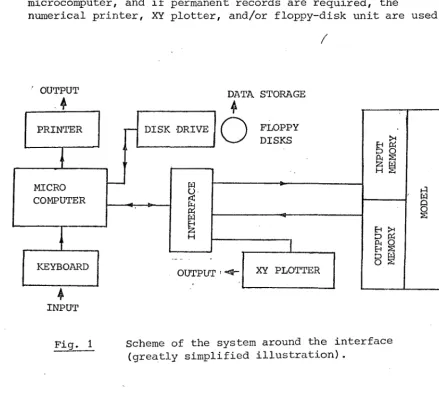
Fig. 1 shows the scheme of the system (relevant parts to the interface only are shown). The following conditions are required for the interface:
Commodore Model -8032 has been chosen for the microcomputer, and Commodore Model 2031 for the floppy-disk driving unit. The choice is mainly due to administrative conditions rather than technical.
_2 The electronic model has 'Input Memory' and 'Output Memory' to and from which the interface is connected. Both the memories can process 8-bit parallel binary numbers between zero and 255
(decimal equivalent), at a speed up to one mega words per second.
2 Input data to the model are supplied through ^ Floppy disks,
b Data line to the microcomputer,
_c Programme in the microcomputer, and/or ^ Keyboard of the microcomputer.
If it is required to store data, floppy disks are used.
^ Output data from the model are displayed on the screen of the microcomputer, and if permanent records are required, the
numerical printer, XY plotter, and/or floppy-disk unit are used.
/
OUTPUT DATA STORAGE
PRINTER
MICRO COMPUTER
DISK DRIVE
KEYBOARD
1
OFLOPPY DISKS
XY PLOTTER OUTPUT
>4 E4 D f > k X S H
A ' w
Q O S EH
n Pi
P4 ( ) X 5 O
[image:5.597.73.513.414.824.2]INPUT
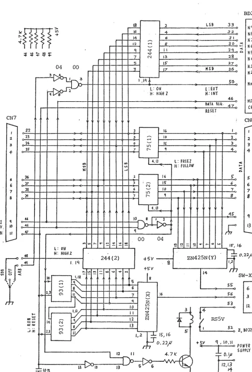
Fig. 2 shows the circuit diagram of the interface, New BD8. This consists of the following four parts:
1 'Output memory' on BD22 3-state output circuit, 244(1) -»
Data bus via CN7 Microcomputer
_2 Sequential-code generator, 93(11 & 93(2) 3-state output circuit, 244(2) -> Data bus via CN7
3 Microcomputer -> Data bus via CN7 -> Data holder, 75(1) & 75(2) -> 'Input Memory' via CN8
^ Microcomputer -> Data bus via CN7 Data holder, 75(1) & 75(2) DAC, 2N425E(Y) XY-plotter via SW-XYP, with X-axis output from 93(1) & 93(2)/ and a pen-lift circuit.
A bidirectional 8-line data bus, and only three control lines (EOI, DAV, ATN) are used for linking the microcomputer and the
interface circuit. These control lines are, used for some particular signals from the microcomputer to the interface circuit only, and not for the signals originally defined by these symbols. .
The Output memory can supply data, when required, at a much higher speed than the microcomputer can access. Therefore, data is available at any time a 'data-request signal' is sent from the micro-computer without a hand-shake procedure. The Input memory can accept data at a much higher speed than the microcomputer can send. There-fore it is enough to send data with 'data-ready signal' any time without a hand-shake procedure. These conditions simplify the design of the interface circuit considerably.
Each part works as follows: . Ji Output memory ->• Microcomputer
Switch SW-SEQ/OFF/ARB is set to ARB. This activates 244(1), and makes BD22/C8 and BD22/N17 controllable (see Appendix 1 for details). A reset signal which is programmed by the microcomputer is sent to BD22/C8 via ATN line. A data-request signal which is programmed by the microcomputer is sent to BD8/N17 via DAV line, for each word of data. The rest of the parts on BD8 do not interfere with the data bus.
2 Sequential-code generator Microcomputer
A reset signal which is programmed by the microcomputer is sent to the sequential generator, 93(1) & 93(2), via ATN line. A logic high signal which is programmed by the microcomputer is sent to gate 00/10 via EOI line. The same signal is also sent to gate 00/9 in order to disable 244(1). Data-request signals which are generated by the microcomputer are sent to gate 00/9 via DAV line in order to refresh the number of the code generator.
2 Microcomputer Input memory
Data are generated by the microcomputer, and fed into the data bus. Switch SW-SEQ/OFF/ARB is set to OFF (neutral position) in order to make both 244(1) and 244(2) disable. Data enters into the input memory via CN7, data holder 75(1) & 75(2) , and CN8. A logic high signal which is programmed by the microcomputer is sent via EOI line to gate 00/10 and activates it. A data-ready signal which is programmed by the microcomputer is sent to gate 00/9 with each word of the data. This signal holds the word in 75(1) & 75(2) during which time the word is entering into the memory, and also
refreshes the memory address. The same data is fed into DAC ZN425E(Y) simultaneously, but this is not intended to be used in this mode of operation.
Data are represented by binary numbers between 0000 0000 and 1111 1110 (decimal 254). The start and end of a set of data are represented by 1111 1111 (decimal 255). This arrangement was started at the time when punched tapes were used. How the start and end codes are detected from the data bus is explained in Appendix 2.
4 Microcomputer XY plotter
The circuit configuration of this mode of operation is the same as _3, but the programme has been designed to make the data-sending speed slower than so that it can be followed by an XY plotter. DAC ZN425E(Y) is used for this operation in order to obtain an ana-logue output from the Y output terminal of SW-XYP. The sequential codes are converted into an analogue voltage by DAC ZN425N(X), and used for the X component input (time axis) of the XY plotter. The above ATN and DAV signals are combined by gate 00/11, and used for the Z input (pen lift or drop) of the XY plotter. Z circuit
(terminals Z and Z') is isolated by a relay so that an arbitrary voltage can be used for the pen drive.
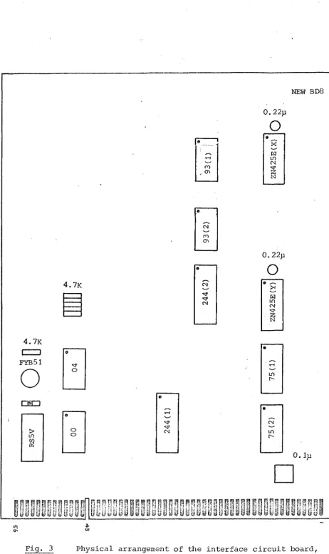
Fig. 3 shows the physical design of the new BD8. The circuit board has the same dimensions as the previous BD8 (the board for the tape punch circuit) so that this can be replaced by the new board. A large unused area now remains on the board which could be used for any further modifications. Table 1 shows the connections of new BD8.
3: ^ tp ^ ? CN7 2 3 f 5 6 7 8 22 23
. 24
iff 26 27 33 EOI DAr
A T N
S 10 44 o' rti -5—<-13 16 J± 12 _1 7 5 CN 1 ,11
LSB 33
4 e ^2 _
6
a
11 2^ .
13 28 _
IS- 27 .
17 MSB 26 o
ro L: ON
H: HISH Z
L:EXT H.-INT
4 6 DATA ? £ « .
RESET -421<, NS N8 N 7 N 6 N 5 N 4 N5 N 2 Nl4 N17 C8 in 16 16 I? 4,13 LD 16 I? to 4.13
L : FREE2 H ; FOLLOW
CN8 1 2 3 4 4f
S5-, 16
00 04 L: ON
H . HISHZ
ZN425N(Y) 244(2)
3_ jc. 16
^ - 10.11 4.7K
i P.2a^
SW-XYP 6 3 (2. Y X Z'
:« Z, BD22/N22
^ POX/ER
[image:8.596.37.531.47.774.2]SUPPLY
Table 1 Terminal connections of the interface, NEW BD8.
Pin No. Colour Function Connector Connected to 1 2 3 4 5 6 7 8 Bn R Or y Gn Be V Gy l(lSB) 2 3 4
^ Data 6 7 8(MSB) C38/1 2 3 4 5 6 7 8 CHIO3/I 2 3 4 5 6 7 8 BN8/N1 N2 N3 B 4 W5 IT6 H7 H8 9 10 11 12 13 14, Bk H 11 Gn ti II +5V 11 II Common \\ V 15 16 17 18 19 20 21 22 Gy V Be Gn Y Or R Bn
8 (MSB) 7 6
5 Data 4 3 2 l(LSB) cm7/8 7 6 5 4 3 2 1 CN7/8 7 6 5 4 3 2 1 GPIB/16 15 14 13 4 3 2 1 23 25 26 27 28 29 30 31 32 33 Gy V Be Gn Y Or R Bn 8(KSB) 7 6
5 Data 4 3 2 l(LSB) — BD22/2 3 4 5 - 6 7 8 9 34 43 44 45 46 47 Gy/R Gy/Be Gy/Bn Gy/Gn EOI Fa DAV ATN CN7/9 CH8/9 CN7/10 CH7/11 GNIO3/9 B m 2 2 / m 7 3D22/C8 GP13/5 M1/C22 GPIB/6 11 48 49 Gy/Bk Y/R
5 6 3D22/N14
52 53 54 55 , 56
Or/On Or/Be Gn Or/R Or/Bn Z Z» Common Y X BD22/N22 5W-XYP/12 ON 2/14 SW-XYP/6 SW-XYP/3
NEW BD8
ri
0.22p
o
X
H m I
4 . 7K
I 1 FYB51
o
ca=]> m
4.7K
o
o
o (N
fO
(N
CM
0,22p
o
H m CM
1
in
(N in
0. Ip
RRRBBBBnnrnBBPFRRP q^nmnnRRmqp
r: p f, n P p
WuULukU8dWUUkUwUWUbdwU8UWU8d@
I'lN uUWWwdUbUuJU UkL&8W85WUut
[image:10.599.52.515.24.803.2]Ul
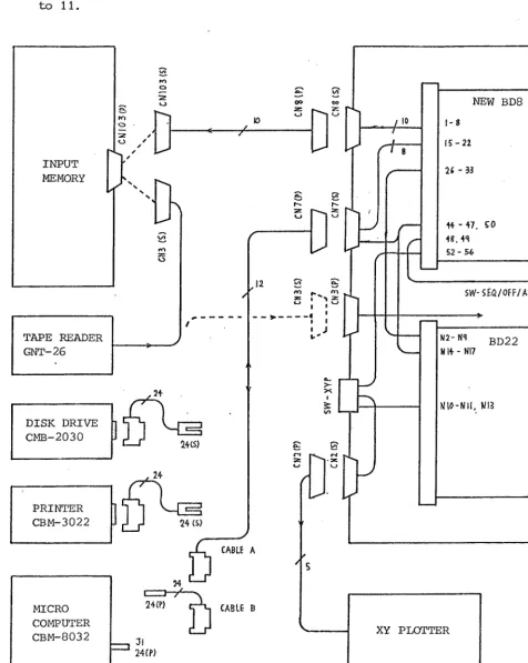
4. COMBINED USE OF INSTRUMENTS
Fig. 4 shows the possible combinations of some instruments related to the interface circuit. The instruments are linked by cables with connectors, since each instrument-has to be operated individually or has to be used for other projects. Details of each connector or related board are shown in tables on pages 10 to 11.
INPUT MEMORY
MICRO COMPUTER CBM-8032
A
TAPE READER GNT-26
DISK DRIVE CMB-2030
PRINTER
CBM-3022
i f ? "
wcs)2 4 <S)
%
.12
" :
>• X
r
X-, CABLE A
34
2 4 (P)
24 CP) c _ r
CABLE B
10 n%
/ —
r
NEW BD8
1 - 8
15-22
li - 3 3
44-47. CO 48, 44
5 2 - 5 6
SW-SEQ/OFF/ARB
-a
N2-N1
N14 - N17
BD22
WIO-NII, m
[image:11.595.41.518.170.767.2]XY PLOTTER
Table 2 Terminal connections related to the interface, NEW BD8
CN2 Pin No.
1 Bn SW-XYP/l X
2 R 8W-XYP/4 Y
3 Or B D 2 2 / m 2 Z 4 Y SW-XYP/lO Z' 5 Be BD22/N15 CRO X 6 V BD22/lfl6 CRO Y 7-13
-14 Gn Common
CN7 Pin No.
1 Bn BD8/22 Data 1
2 R 21 2
3 Or 20 3
4 • Y 19 4
5 Gn 18 5
6 Be 17 6
7 V 16 7
8 Gy 15 8
9 Br/Gy 44 EOI
10 R/C^ 46 DAY
11 Gn/Gy 47 ATN
12 —
13 Gn Common C1T8
Pin No.
1 BD8/33 Data 1
2 R 32 2
3 Or 31 3
4 Y 30 4
5 Gn 29 5
6 Be 28 6
7 V 27 7
8 Gy 26 8
9 Be/Gy 45 FH
10-12
13 Gn Common
BB22 (Modified parts only) Pin Fo.
NIO Bn SW-XYP/l Nil R SW-XYP/2 N12 Or cm2/3 N13 Y SW-XYP/4
N14 Gy/R ?D8/44 EOI N17 Gy/Bn BD8/46 DAV
11 8W-%Yr Pin iTo. 1 2 3> Bn Bn Or/Sn BD22/N10 CN2/1 BD8/N56 X 4 5 6 R R Or/R
B D 2 ^ N 1 1 CN2/2 BD8/N55
Y
7-9
-10 11 12 Y Y Or/se
B D 2 2 / m 3 CN2/4 BD8/N53
Z'
SW-XYP 1 2 3 4 5 6 7 8 9 10 11 12
Pin view
Cable A
IEEE488 Connector CF7 Connected to Pin llo.
1 Bn 1 Bn BD8/22 Bat a 1
2 11 2 R 21 2
3 Or 3 Or 20 3
4 Y 4 Y 19 4
5 Gn 9 P BD8/44 EOI
6 Be 10 Bk 46 DAV
7 V
-8 Gy —
9 ¥ —
10 W/Be
BD8/47
11 W/Bn 11 E -Be BD8/47 ATIT
12 Screen 24
13 W/Or 5 Gn BD8/18 Data 5
14 W/Y 6 Be 17 6
15 W/Gn 7 V 16 7
16 If/Gn 8 Gy 15 8
17 w / v
-18 W/Gy 25
19 W/Bn/Be 25 • ¥ Common
20 W/R/Be 25
21 w/Or/Be 25
22 W/Y/Be 25
5. D E S I G N O F S O F T W A R E
Software for interface NEW BD8 has been developed as follows:
PROG D1 Interface Screen (Test) PROG D2 Model Screen (Operational) PROG D3 Screen ->• Disk (Operational) PROG D4 Disk ->• Screen (Operational) PROG D5 Screen Printer (Operational) PROG D6 Screen Model (Basic form)
PROG D7 Screen Model (Test, 2 channels) PROG D8 Screen Model (Test, 144 channels) PROG D9 Screen ->• XY plotter (Operational)
PROG D20X Uniform wind field in X direction PROG D20Y Uniform wind field in Y direction
PROG D20J Uniform pressure-gradient field in X direction
P R O G D20K Uniform pressure-gradient field in Y direction
Some of the programmes are for testing the performances of the interface circuit including the microcomputer, disk, printer and model. Others are for actual operations. All the programmes are
stored on a floppy disk. If a waveform can be expressed mathemati-cally, only a formula (or formulas) is stored on the disk and the waveform is generated for each operation, rather than storing the whole amount of data for the waveform.
The total number of data in a section of some programmes can be varied if required. In this chapter, 256 is used for these examples.
A switch, S W - S E Q / O F F / A R B (on the front panel of the control
13
PROG D1 INTERFACE SCREEN (TEST)
A programme for testing the transmission of data from interface BD8 to the microcomputer screen, by using sequential numbers.
Set SW-SEQ/OFF/ARB to SEQuential.
After the programme is run, if sequential numbers 0 to 255 are displayed on the screen, the transmission is perfect.
Programme Comments
18 POKE 59456,8 28 FOR N=0 TO 255 38 m=PEEK(59424) 48 POKE 5G88+H,A 58 E=PEEK(58e8+N) 68 PRINT
78 POKE.59427,68 88 POKE 59427,52 98 NEXT
188 POKE 59456,4 118 STOP
ATN —> L Counter
Read data received from data "bus Store data in screen memory
Read data from screen memory Display data on screen
DAY -H- H>
PROG D2 MODEL 4- SCREEN (OPERATIONAL)
A programme for transferring an arbitrary waveform from the model to the microcomputer screen in an actual operation.
Model Output memory
Select SW-BIP/MON, BIRolar or Monopolar depending on the waveform. Set SW-INT.C/EXT.C to EXTernal Clock (generated in the Input MemoryI, Set SW-MAGNIF to 1, 2, 5, 10, or 20, depending on the amplitude of the waveform.
Set SW-WRITB/PLOT to WRITE. Press the red button near the switch. Monitor the waveform on a CRO.
Output memory ->• Microcomputer Set SW-SEQ/OFP/ARB to ARBitrary.
Select SW-96/256 depending on the length of data.
Load PROG D2 to the microcomputer. Then fix the maximum number in Line 30-.
V Programme Comments
18 POKE 59489,52 28 POKE 59456,8
EOI L ATN L 38 FOR N=8 TO 255
48 m=PEEK(59424) 58 POKE 5888+N,m 68 E=PEEK(5888+N) 78 PRINT B;
Counter (Maximum 255) Read.data on data "bus. To screen memory
Read data on screen memory Display data on screen 88 POKE 59427,52
98 POKE 59427,68 188 NEXT
Next data-request signal
110 POKE 59489,68 128 POKE 59456,4 138 STOP
15
PROG D3 SCREEN -> DISK (OPERATIONAL)
A programme for transferring data on the microcomputer screen to a disk, in a,n actual operation.
Set SW-SEQ/OFFyARB to OFF.
Programme Comments
10 DOPEH#l,"DmTAFILE",W 20 FOR 1=5888 TO 5255
M=PEEK(I) 40 PRIHT#1,M 50 NEXT
60 DCL0SE#1 70 STOP
Open sequential file on disk to write Screen memory address in loop
Get. contents of Lst memory address Store contents on disk
PROG D4 DISK -> SCREEN (OPERATIONAL)
A programme for transferring data from a disk to the microcomputer screen, in an actual operation.
set SW-SEQ/OFFyARB to OFF.
Programme Comments
10 D0PEH#1,"DATAFILE",R 2 0 FOR 1=0 TO 2 5 5
38 IHPUT#1,I 48 POKE 5080+1,1 50 N = P E E K ( 5 0 0 0 + I ) 60 PRINT NJ
70 NEXT I 8 0 DCL0SE#1 98 STOP
Oper sequential file on disk to read .Counter for 255 words
Get 1st word from disk 1st word to screen menory Display word to check
17
PROG D5 SCREEN -> PRINTER (OPERATIONAL)
A programme for transferring data from the microcomputer screen to the printer, in an actual operation.
Set SW-SEQ/OFI^/ARB to OFF,
Programme Comments
18 OPEN.2,4 20 CMD 2
30 FOR 1=5800 TO 5255 40 M=PEEK(I)
50 PRINT#2,M; 60 NEXT
70 CLOSE 2 80 STOP
Open channel to printer
Screen memory address in loop Read contents in memory
PROG D6 SCREEN -> MODEL (BASIC FORM)
A programme for transferring data from the microcomputer screen to the 'Input Memory' of the electronic model.
Set SW-SEg/OFF/ARB to OFF.
Programme , Comments
10 POKE 59409,60 20 POKE 59426,255
BOI ->• H
Start sifmal '2SS' 30 FOR 1=5000 TO 5255
40 M=PEEK(I) 50 PRINT M; 60 POKE 59426,M
Loop to get 256 words from memory Get word from screen memory address
Display 1st address contents to check Transfer contents to data "bus
70 POKE 59427,52 80 POKE 59427,60 90 NEXT I
DAV —4- L \ ^ , , . ^ DAV Data--rready signal Next number from rnemorv ' 100 POKE 59426,255
110 POKE 59426,0 120 STOP
End signal '255' Return to zero
19
PROG D7 SCREEN -X MODEL (TEST, 2 CHANNELS)
A programme for testing the performance of the interface and input memory, by using a standard waveform for 14emory channels 0 and 1.
Set SW-SEQ/OFP/ARB to OFF.
Programme Comments
' 10 POKE 59409,60 EOI H
20 FOR H=255 TO 254 STEP -1 30 PRINT H;
40 POKE 59426,H 50 POKE 59427,52 60 POKE 59427,60 70 NEXT H
Start signal '255') and data 254 Display number on screen
Humher to data bus
D AV —»• L \ .
DAV — g / Data-ready signal
80 FOR 1=254 TO 0 STEP -1 90 PRINT I;
100 POKE 59426,I 110 POKE 59427,52 120 POKE 59427,60 130 NEXT I
Sequential numbers 254 to 0
140 FOR J=0 TO 254 150 PRINT J;
160 POKE 59426,J 170 POKE 59427,52 180 POKE 59427,60 190 NEXT J
Sequential numbers 0 to 254
200 FOR K=254 TO 255 210 PRINT K;
220 POKE 59426,K 230 POKE 59427,52 240 POKE 59427,60 250 NEXT K
Data 254) and end signal '255'
260 POKE 59426,0 270 STOP
Data bus to zero
Press the red button on the input memory panel, for displaying the waveform on a CRO.
W a v e f o r m 2SS 254
START / k
(HANWEl
20
PROG D8 SCREEN -> MODEL (TEST, 144 CHANNELS)
A programme for testing the performances of the interface and input memory, by using a standard waveform for memory channels 0 to 143.
Set SW-SEQ/OFF/ARB to OFF.
Programme Comments
18 POKE 59409,60 20 S=0
EOI H
Set counter to zero 30 POKE 59426,255
40 POKE 59427,52 50 POKE 59427,60
Start signal '255' to data bus dIv % y) Data-i^eady signal 60 FOR B=8 TO 253
70 POKE 59426,B 80 POKE 59427,52 90 POKE 59427,60
100 NEXT B
Set" up loop
Number to data bus
DAY -4. L. _ . , . ,
DAV —^ Data-ready signal
110 FOR C=1 TO 4 120 POKE 59426,254 130 POKE 59427,52 140 P O K E 59427,60 150 NEXT C
Set up loop
Number to data bus
D AV —=> L \ ^ , , . ^ DAV g) Data-ready signal
160 FOR E=253 TO 0 STEP -1 170 POKE 59426,E
180 POKE 59427,52 190 POKE 59427,60 200 NEXT E
Set up loop
Number to data bus
DAY —•> L\ * , , . , DAV -J- H' Data-ready signal
210 S=l+S
220 IF S<72 GOTO 60 230 POKE 59426,255 240 STOP
Increment counter Test counter
End signal ' 255' to dg,ta bus
This, programme does not display data on the microcomputer screen, hence the cursor disappears from the screen, until the whole process is completed. The data can be monitored as an analogue waveform by a CRO through the monitor terminals of the input memory. After the process has been completed, press the red button on the input memory, panel in order to turn the memory into a read mode.
Waveform 251 zs* START CHANNEL 0
256 INCS
A
21
PROG D9 SCREEN XY PLOTTER (OPERATIONAL)
A programme for transferring data from the microcomputer screen to an XY plotter, in an actual operation.
Set SW-SEQ/OFF/ARB to OFF. Set SW-XYP to MICROCOMP.
Programmes Comments
0 FOR A = 8 TO 254 2 P O K E 5G08+A,A 4 NEXT H
)
< Sequential numbers to test ^ main programme "below line 10 18 P O K E 59459,4
20 POKE 59456,0 30 POKE 59409,60
I S Z l) Beset ADO EOI H
40 FOR 1=5000 TO 5255 . 5 0 M = P E E K ( I )
60 P R I N T M; 70 P O K E 5942G,M
Loop to get 256 words from memory-Get word from memory address Display 1st address to check Transfer contents to data "bus 80 P O K E 59427,52
90 P O K E 59427,60
DAV —>- L\ _ , _ _ ])AV F'' ^8.ta-ready signal 100 FOR C=1 10 5 0
110 NEXT C 120 NEXT I
130 P O K E 59426,0 140 STOP
For reducing processing speed Next number from memory
Return to zero
Replace programme lines 0. to 4 by an appropriate programme for an actual operation.
Choose the last number in programme line 90 for an appropriate speed for
the JXY, plotter used.
There is no control on BD8 for the magnification of X and Y outputs. Use controls on the XY plotter, if required.
PROG D20X
PROG D20Y
PROG D20J
PROG D20K
UNIFORM WIND FIELD IN X DIRECTION UNIFORM WIND FIELD IN Y DIRECTION
UNIFORM PRESSURE-GRADIENT FIELD IN X DIRECTION UNIFORM PRESSURE-GRADIENT FIELD IN Y DIRECTION (ALL OPERATIONAL)
A set of programmes used for the computation of storm surges due to two uniform wind fields in orthogonal directions (X and Y), and two uniform pressure-gradient fields in orthogonal directions
(J and K). Note, J and K are the same directions as X and Y respectively, but the different symbols are used in order to indicate that they,are pressure-gradient fields.
X and Y have a uniform pulse height (254") in their programmes. J and K have different pulse heights in each section depending on each geographical position in the sea area. The value of each pulse in J and K is given in the DATA lines in the programme. The physi-cal meaning of the whole set of programmes and how the values are determined have been described in a separate paper.
The values in this set of programmes represent the values for the North Sea area including the sea around the north part of Scotland. Should the area to which a wind or pressure field is applied be smaller than this area, the values representing the out-side of the smaller area should be zero in the programme.
Waveforms
X
355
J I
3S5 554
J 5 5
-J L
K 555
t HAtT
I I ' IHtS '
_ _ L
I
J
--1
- L
I
/3S
END
I
PROG D20X
23
Programme Comments
10 S = 8
20 POKE 59409,cm
Set counter to zero EOI H
38 K=255
48 POKE 59426,K 58 PRINT K;
Start signal '255' To data "bus
Display on screen 68 H=8
78 FOR L=1 TO 128 88 POKE 59426,A 98 POKE 59427,52 188 POKE 59427,68 118 PRINT A;
128 NEXT L
Set up loop
Number to data bus
DAY L\ , J . ,
Data-ready signal JJAV — x i
Display on screen IdW B=^:b4
148 FOR P=1 TO 128 158 POKE 59426,B 168 POKE 59427,52 178 POKE 59427,68 188 PRINT BJ
198 NEXT P
Set up loop
Number to data bus
Data-ready signal jJAV — 1 1
Display on screen 288 FOR C=1 TO 256
218 POKE 59426,A 228 POKE 59427,52 238 POKE 59427,68 248 PRINT m;
258 NEXT C
Set up loop
Ntimber to data bus
Data-ready signal JJAV —» n
Display on screen y=l+b
278 IF S<4 GOTO 88 288 POKE 59426,K 298 PRINT K; 388 STOP
Increment counter Test counter
PROG D20Y
Programme Comments
1 y b'~U
2 0 P A K E 59409.nO
Set counter to zero BOI E
3 8 K = 2 5 5
4 0 P O K E 59426,K 50 P R I N T K;
Start signal '255' To data "bus
Display on screen 60 A = 0
70 FOR L=1 TO 3 8 4 8 0 P O K E 59426,H 90 P O K E 5 9 4 2 7 , 5 2 100 P O K E 5 9 4 2 7 , 6 0 110 P R I N T A;
120 N E X T L
Set up loop
Number to data "bus
DAV — ' L n _ , J . ^ DAV —> H' ^8.ta-ready signal Display on screen
130 B = 2 5 4
140 FOR P=1 TO 128 150 P O K E 59426,E 160 P O K E 5 9 4 2 7 , 5 2 170 P O K E 5 9 4 2 7 , 6 0 180 P R I N T B;
190 N E X T P
Set up loop
Bumber to data bus
DAV g ) Data-ready signal Display on screen
200 5 = 1 + S
210 IF S { 2 GOTO 78 220 P O K E 59426,K 2 3 0 P R I N T K; 240 S T O P
Increment counter Test counter
25
PROG D20J
Programme Comments
18 DATA 851,888,898,114,149,875,110,130,131,126, 20 DATA 076,114,126,127,288,890,088,078,198,238, 30 DATA 080,070,867,215,859,041,855,855,225,045, 48 DATA 844,839,872,839,836,019,063,877,024,016, 5ti DATA 115, w6w, Li63,116,870, 814,839.• 827,115,894, 60 DATA 021,831,838,078,831,819,032,826,833,3 64, 78 DATA 828,166,218,113,869,876,874,864,008,000, 80 DATA 000,888 '
188 S=8
118 POKE 59489,68
Set counter to zero EOI H
128 K=255
130 POKE 59426,K 140 PRINT K;
Start signal '255' To data "bus
Display on screen 158 A=0
160 FOR L=1 TO 128 170 POKE 59426,A 180 POKE 59427,52 190 POKE 59427,60 200 PRINT A;
210 NEXT L
Set up loop
Num'ber to data line
DAV — I i \ Ti J- J • T DAV Ir ])8.ta-ready signal Display on screen
228 READ B
238 FOR P=1 TO 128 240 POKE 59426,8 250 POKE 59427,52 260 POKE 59427,60 270 PRINT B;
280 NEXT P
Read data value Set up loop
dumber to data "bus
DAV — L \ „ . J. . , ]>A.V ->>• H' Data-reading signal Display on screen
290 FOR R=1 TO 384 308 POKE 59426,A 318 POKE 59427,52 328 POKE 59427,68 330 PRINT A;
348 NEXT R
Set up loop
Number to data bus
BAV Data-ready signal Display on screen
J DO i>=l+b
368 IF S<4 GOTO 228 378 POKE 59426,K
380 PRINT K; 390 STOP
Increment counter Test counter
PROG D20K
Programme Comments
10 DATA 0 5 1 , 0 8 0 , 0 9 8 , 1 1 4 , 1 4 9 , 0 7 5 , 1 1 0 , 1 3 0 , 1 3 1 , 1 2 6 , 20 DATA 0 7 6 , 1 1 4 , 1 2 6 , 1 2 7 , 2 0 8 , 0 9 0 , 0 8 8 , 0 7 8 , 1 9 0 , 2 3 8 , 30 DATA 0 8 0 , 0 7 0 , 0 6 7 , 2 1 5 , 0 5 9 , 0 4 1 , 0 5 5 , 0 5 5 , 2 2 5 , 0 4 5 , 4 0 DATA 0 4 4 , 0 3 9 , 0 7 2 , 0 3 9 , 0 3 6 , 0 1 9 , 0 6 3 , 0 7 7 , 0 2 4 , 0 1 6 , 50 DATA 1 1 5 , 0 6 0 , 0 6 3 , 1 1 6 , 0 7 0 , 0 1 4 , 0 3 9 , 0 2 7 , 1 1 5 , 0 9 4 , 60 DATA 0 2 1 , 0 3 1 , 0 3 8 , 0 7 0 , 0 3 1 , 0 1 9 , 0 3 2 , 0 2 6 , 0 3 3 , 1 6 4 , 70 DATA 0 2 0 , 1 6 6 , 2 1 8 , 1 1 3 , 0 6 9 , 0 7 6 , 0 7 4 , 0 6 4 , 0 0 0 , 0 0 0 , 8 0 DATA 0 0 0 , 0 0 0
100 S = 0
110 P O K E 5 9 4 0 9 , 6 0
Set counter to zero BOI H
120 K = 2 5 5
130 POKE 59426,K 140 P R I N T KJ 150 A = 0
Start signal '255' To data "bus
Display on screen 160 FOR L=1 TO 3 8 4
170 P O K E 59426,A 180 P O K E 5 9 4 2 7 , 5 2 190 P O K E 5 9 4 2 7 , 6 0 200 P R I N T A;
210 N E X T L
Set up loop
ITumber to data "bus
DAV — L \ ^ ; J . _
DAV —9- Ir signal
Display on screen 220 R E A D B
2 3 0 FOR P=1 TO 128 2 4 0 P O K E 5 9 4 2 6 , B 2 5 0 P O K E 5 9 4 2 7 , 5 2 2 6 0 P O K E 5 9 4 2 7 , 6 0 270 P R I N T B;
280 NEXT P
Read data value Set up loop
Eumber to data "bus DAY Ln
DAY
Display on screen 290 S = l + S
300 IF S < 4 GOTO 160 310 P O K E 59426,K 320 P R I N T K; 330 STOP
Increment counter Test counter
27
CONCLUSION
28
Appendix 1 TIMING ARRANGEMENT IN BD22
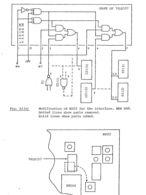
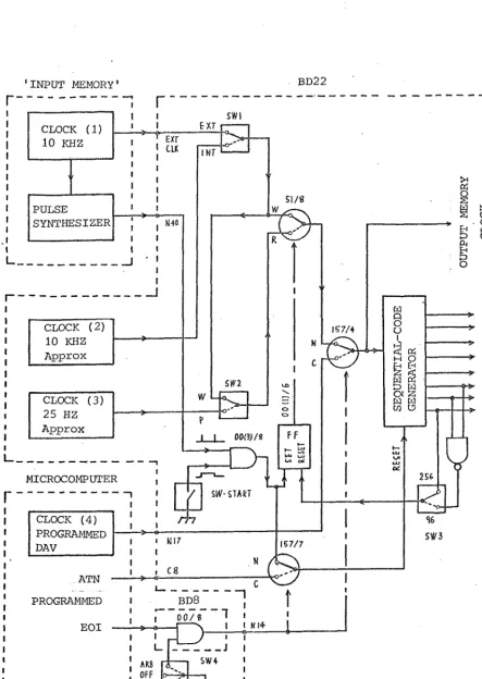
The interface circuit BD8 (shown in Fig. 2) is connected to BD22 through which the output of the model is taken. Details of BD22 have been described in IOS Internal Document 85 (1980). Minor modifications have been carried out to BD22 in order to combine, it with the newly designed BD8 in 1982, as shown in Fig. Al(a) and Al (b) .
BD22 is essentially an ADC plus a memory. However, the timing arrangement of BD22 is rather complex as shown in Fig. A2 (greatly simplified illustration, but the new modifications are included). This is due to the following conditions:
1 The write rate and start/end signals of the memory on BD22 should be synchronized with those of the 'Input Memory' when an approximate timing (order of seconds) of the start is commanded manually by a push button.
2 The memory on BD22 should have three clock rates for reading: ^ fast rate for a CRO,
b • medium rate for the microcomputer, and c_ slow rate for a XY plotter.
_3 Without any external clocks, BD22 should work with its own two clocks, with fast and slow rates.
The timing control of BD22 shown in Fig. works as follows: Manual switch SWl selects the sources of the write clock, EXT
(clock _1 in the Input Memory) or INT (clock 2^ within BD22) . Manual switch SW2 selects Write or Plot mode of the memory on BD22, with the start command by SW START. Only when SW START is pressed, pulses from the pulse synthesizer passes through gate 00(3)/8. Details of the pulse synthesizer, through which the operation of the model is .linked to BD22, are described in lOS Internal Document 160 (1982).
The output of gate 00(3)/8 sets FF 00(1)/6 and controls the elec-tronic switch 51/8, either Write or Read mode. The output of 51/8 enters into the sequential code generator and other circuits, through selector 157/4, until the FF is reset. This reset signal is given when the generator completes a sequence of codes, up to 95 or 255 depending on the setting of SW3. The sequential generator is reset by a pulse through selector 157/7, before it starts.
The microcomputer is linked with BD22 only when selectors 157/4 and 157/7 are switched to the microcomputer side. Such a state occurs only when gate 00/8 on BD8 is activated by SW4 (ARB side) and EOI signal. When the two selectors are switched to the microcomputer side, the read clock is generated by the microcomputer and enters into selector 157/4 through terminal Nl7; also the reset signal enters into selector 157/7 through terminal C8. Note the write
29
• PART OF 74LS157
rh
NI4 N17
in o
o
L _
CN
Fig. A1 (a) Modification of BD22 for the interface, NBIV BD8. Dotted lines show parts removed.
Solid lines show parts added.
74LS157
[image:31.604.55.548.90.749.2] [image:31.604.57.499.94.440.2]30
'INPUT MEMORY' BD22
SWI EXT
INT
El/8
O 157/4
003J/8
11
MICROCOMPUTER
SW START
IE 7/7
A T N
BD8
0 0 / 8 1
PROGRAMMED EOI
ARB
OFF SEQ CLOCK (4)
PROGRAMMED DAV
CLOCK (2) 10 KHZ Approx
CLOCK (3) 25 HZ Approx PULSE
SYNTHESIZER CLOCK (1)
10 KHZ
[image:32.602.59.502.48.672.2]H O
31
Appendix 2 START AND END SIGNALS FOR THE INPUT MEMORY
Data can be fed into the input memory either by a punched-tape reader or the microcomputer with the interface BD8. This arrange-ment has been used because a number of punched tapes were already made prior to the floppy disk being employed. The input memory is linked with the tape reader or BD8 by 8 parallel data lines and a single timing signal line only. Therefore, the start and end of the data transmission are indicated by 1111 1111 (decimal 255) on the data line (255 is not used for data). Fig. A3 shows the circuit for detecting the start and end signal from the data line. The first 255 is regarded as Start, and the second as End.
i
H
g
g
B S
TIME SIGNAL
DATA BUS
POWER-ON SIGNAL SW-START
LED Reset
TAPE START
FREQ DIVIDER
S
e
H
g
Appendix 3 LOCATION OF SWITCHES
€ )
& ® ( b ®
AOS PAS AIT n.o; *xif*ON
^ 3 — ^
, € )
Of —' / \y/%0 Off
m e - ©
Control cabinet
Front panel
SEQ/OFF/ARB WRITE/PLOT INT.C/EXT.C BIP/MON
MODEL
POWER XYP
MICROCOMP
Rear panel
SW-96/256
0
•
96256
Component side of BD22 Input-gain