University of Warwick institutional repository:
http://go.warwick.ac.uk/wrap
A Thesis Submitted for the Degree of PhD at the University of Warwick
http://go.warwick.ac.uk/wrap/66735
This thesis is made available online and is protected by original copyright.
Please scroll down to view the document itself.
I N VE R I T A S
U N
I VE
R S
I T AS WAR WI CE
NS
I S V I N O
Low Temperature Semiconductor-Superconductor
Junctions & Their Optimisation
by
James Sedgwick Richardson-Bullock
Thesis
Submitted to the University of Warwick
for the degree of
Doctor of Philosophy
Department of Physics
Contents
Acknowledgments v
Declarations vii
Abstract viii
List of Publications ix
List of Tables xiv
List of Figures xv
Abbreviations and Symbols xxv
1 Introduction 1
1.1 The need for cryogenics . . . 1
1.2 Thermoelectric cooling and the alternatives . . . 3
1.3 Tunnel junction coolers . . . 5
1.3.1 The superconducting band gap . . . 5
1.3.2 Normal metal - insulator - superconductor junctions . . . 7
1.3.3 Semiconductor - superconductor junctions . . . 8
1.3.4 Double junctions . . . 9
1.4 Tunnel junction theory . . . 10
1.4.1 Metal-semiconductor contacts . . . 10
1.4.3 Cooling power . . . 17
1.4.4 Sub-gap leakage and the Dynes parameter . . . 19
1.4.5 Carrier-phonon coupling . . . 21
1.4.5.1 Modification through strain . . . 23
1.4.5.2 Hole systems . . . 27
1.4.6 Heating powers . . . 27
1.4.6.1 Joule heating . . . 27
1.4.6.2 Quasiparticle heating . . . 28
1.4.6.3 Andreev heating . . . 30
1.4.7 Power balance equation . . . 31
1.5 Tunnel current thermometry . . . 31
1.5.1 Thermometer bias current . . . 35
1.5.2 Thermometer saturation . . . 35
1.5.2.1 Γ induced saturation . . . 35
1.5.2.2 Thermometer current induced saturation . . . 37
1.5.3 Non-empirical tunnel current thermometry . . . 39
2 Fabrication techniques 41 2.1 Sm-S junction fabrication . . . 41
2.2 Sm-I-S junction fabrication . . . 42
2.3 Vanadium junction fabrication . . . 43
2.4 PtSi junction fabrication . . . 43
3 Experimental techniques and equipment 47 3.1 Cryostats . . . 47
3.1.1 Closed Cycle . . . 47
3.1.2 Heliox AC-V . . . 48
3.1.2.1 Multi-sample stage . . . 49
3.1.3 Dilution refrigerator . . . 51
3.2 Electrical characterisation techniques . . . 52
3.2.1 Hall effect . . . 52
3.2.1.1 Van der Pauw method . . . 53
3.2.1.2 Hall bar method . . . 54
3.2.1.3 Common voltage errors . . . 55
3.2.2 Transfer length method . . . 56
3.2.2.1 Contact End Resistance . . . 57
3.3 Electron cooling measurements . . . 58
3.3.1 Treatment of errors . . . 59
3.4 Carrier-phonon coupling measurements . . . 60
3.4.1 DC method . . . 60
3.4.2 AC method . . . 60
3.4.3 Treatment of errors . . . 61
3.5 Structural characterisation methods . . . 62
3.5.1 Transmission electron microscopy . . . 62
3.5.2 Focused ion beam scanning electron microscopy . . . 63
4 Alternatives to aluminium superconducting contacts 67 4.1 Vanadium . . . 69
4.2 Platinum Silicide . . . 76
4.3 Summary . . . 88
5 Hole-Phonon coupling 89 5.1 Extracted coupling and the observed power law . . . 91
5.2 Theoretical considerations . . . 94
6 Semiconductor-insulator-superconductor junctions 98
6.1 Oxidation studies and Sm-I-S junction characterisation . . . 99
6.1.1 Junction quality . . . 105
6.1.2 Sm-I-S Tunnel junction cooling . . . 107
6.2 Summary . . . 116
7 Strained semiconductor-insulator-superconductor junctions 117 7.1 Summary . . . 124
8 Further work 126
Acknowledgments
I would like to thank each of my supervisors, Professors David Leadley, Terry Whall
and Evan Parker for their continued encouragement.
Special thanks go to Dr. Martin Prest for his constant support and
com-radery. His techno-wizardry made this project possible.
Doctors David Gunnarsson, Mika Prunnila, Juha Muhonen and Hung Nguyen
made for excellent collaborators and I am greatly indebted to them for the work
that they carried out on my behalf, as well as their efforts to make me feel welcome
in a strange and mystical Finland.
Closer to home, the members of the University of Warwick’s Nano-Silicon
group have each been helpful and entertaining in their own way. Particular mention
should be made of Dr. Caterina Casteleiro and her constant supply of cakes for any
and all occasions. This thesis can be measured in confectionery and I owe her a
debt I doubt I can ever repay.
Lastly, I should like to thank my wife Rachael Richardson-Bullock. Fully
expressing the depth of her care, consideration and patience and the resulting love
‘The scientist does not study nature because it is useful to do so. He
studies it because he takes pleasure in it, and he takes pleasure in it
because it is beautiful. If nature were not beautiful it would not be worth
knowing, and life would not be worth living. I am not speaking, of
course, of the beauty which strikes the senses, of the beauty of qualities
and appearances. I am far from despising this, but it has nothing to do
with science. What I mean is that more intimate beauty which comes
from the harmonious order of its parts, and which a pure intelligence
can grasp.’
Declarations
This thesis is submitted to the University of Warwick in support of the author’s
application for the degree of Doctor of Philosophy. Except where specifically stated,
all investigations and experiments presented herein were carried out by the author
Abstract
The research presented in this thesis focuses on the relatively young field of direct
electron cooling via semiconductor-superconductor tunnel junctions. These devices
utilise the superconducting energy gap to form a high pass electron filter,
capa-ble of lowering the effective electron temperature in the semiconductor electrode.
The presented research focuses on optimizing the performance of such junctions i.e.
the minimum achieved electron temperature, primarily by modifying the electrical
properties of the semiconductor/superconductor and influencing the quality of the
semiconductor-superconductor interface.
In the semiconducting electrode, the effect of carrier type on the thermal
coupling of the system is studied, as is the effect of mechanical strain, induced via
lattice mismatch. A study is made of alternative superconductors, modifying their
properties through the use of thin films for the superconducting contact.
Finally, a comprehensive investigation is presented into the importance of
fabrication procedures on device characteristics, leading to the development of the
List of Publications
Refereed Articles
2014 Advances in Semiconductor Electron Cooling using Improved Su-perconductor Tunnel Junctions
D. Gunnarsson,J. S. Richardson-Bullock, M. J. Prest, N. Hung, A.
Timo-feev, M. Prunnila, T. E. Whall, E. H. C. Parker and D. R. Leadley,in
prepa-ration for submission to Nature Communications.
2014 Comparison of electron-phonon and hole-phonon energy loss rates in silicon
J. S. Richardson-Bullock, M. J. Prest, M. Prunnila, D. Gunnarsson, V. A. Shah, A. Dobbie, M. Myronov, R. J. H. Morris, T. E. Whall, E. H. C. Parker
and D. R. Leadley,accepted for publication in Solid State Electronics.
2014 Superconducting platinum silicide for electron cooling in silicon
M. J. Prest, J.S. Richardson-Bullock, Q. T. Zhao, J. T. Muhonen, D.
Gunnarsson, M. Prunnila, V. A. Shah, T. E. Whall, E. H. C. Parker and D.
R. Leadley,accepted for publication in Solid State Electronics.
2012 Electrical isolation of dislocations in Ge layers on Si(001) substrates through CMOS-compatible suspended structures
V. A. Shah, M. Myronov, C. Wongwanitwatana, L. Bawden, M. J. Prest, J.
S. Richardson-Bullock, S. Rhead, E. H. C. Parker, T. E. Whall and D.
R. Leadley, Science and Technology of Advanced Materials, volume 13, pp.
2011 Strain enhanced electron cooling in a degenerately doped semicon-ductor
M. J. Prest, J. T. Muhonen, M. Prunnila, D. Gunnarsson, V. A. Shah,J. S.
Richardson-Bullock, A. Dobbie, M. Myronov, R. J. H. Morris, T. E. Whall,
E. H. C. Parker and D. R. Leadley, Applied Physics Letters, volume 99, pp.
251908, 2011.
Conference Papers
2014 High Quality Semiconductor-Superconductor Junctions for Ther-mal Detectors and Electron Coolers
D. Gunnarsson,J. S. Richardson-Bullock, M. J. Prest, A. Timofeev, T. E.
Whall, E. H. C. Parker, D. R. Leadley and M. Prunnila,Internationa
Confer-ence on Superconductivity and Magnetism (ICSM).
2014 Strain and Interface Engineered Semiconductor-Superconductor Cool-ers and Detectors
D. Gunnarsson, J. S. Richardson-Bullock, M. J. Prest, A. Timofeev, T.
Brien, M. Kiviranta T. E. Whall, E. H. C. Parker, D. R. Leadley, P. Mauskopf
and M. Prunnila, International Workshop On Low Temperatures Electronics
(WOLTE).
2014 New Concepts in Infra-red Bolometry
E. H. C. Parker, M. J. Prest, J. S. Richardson-Bullock, M. Myronov, T.
E. Whall, D. R. Leadley, T. Brien, P. Mauskopf, D. Gunnarsson, M. Prunnila,
M. Kiviranta and L. Piccirillo,International Workshop On Low Temperatures
Electronics (WOLTE).
2014 High Quality Superconductor-Semiconductor Tunnel Junctions
D. Gunnarsson,J. S. Richardson-Bullock, M. J. Prest, H. Q. Nguyen, T. E.
Whall, E. H. C. Parker, D. R. Leadley and M. Prunnila,European Conference
2013 Electron-Phonon Coupling Engineering for Thermal Devices
M. Prunnila, D. Gunnarsson, J. S. Richardson-Bullock, M. J. Prest, T.
E. Whall, E. H. C. Parker, L. Donetti and F. Gamiz, European Materials
2013 Cooltronics: A new low-temperature tunneling-technology based on Silicon
T. E. Whall, M. J. Prest,J. S. Richardson-Bullock, V. A. Shah, M.
My-ronov, E. H. C. Parker, D. R. Leadley, M. Prunnila, D. Gunnarsson, T. Brien,
D. Morozov and P. Mauskopf,Ultimate Integration on Silicon (ULIS).
2013 Hole-phonon energy loss rate in boron doped silicon
J. S. Richardson-Bullock, M. J. Prest, M. Prunnila, D. Gunnarsson, V. A. Shah, A. Dobbie, M. Myronov, R. J. H. Morris, T. E. Whall, E. H. C. Parker
and D. R. Leadley,Ultimate Integration on Silicon (ULIS).
2013 Novel fabrication technique for Ge membranes
V. A. Shah, M. Myronov, L. Bawden, M. J. Prest, J. S.
Richardson-Bullock, P. M. Gammon, S. Rhead, E. H. C. Parker, T. E. Whall and D.
R. Leadley,Ultimate Integration on Silicon (ULIS).
2013 Using platinum silicide as a superconductor for silicon electron cool-ers
M. J. Prest, Q. T. Zhao, J. T. Muhonen, V. A. Shah, J.S.
Richardson-Bullock, M. Prunnila, D. Gunnarsson, T. E. Whall, E. H. C. Parker and D.
R. Leadley,Ultimate Integration on Silicon (ULIS).
2012 Ultra-High Hall Mobility (1×106cm2V−1S−1) in a Two-Dimensional Hole Gas in a Strained Germanium Quantum Well Grown by Re-duced Pressure CVD
A. Dobbie, M. Myronov, R. J. H. Morris, M. J. Prest, J. S.
Richardson-Bullock, A. H. A. H Hassan, V. A. Shah, E. H. C. Parker, T. E. Whall and
2012 Simple Fabrication of Suspended Germanium Structures and Their Electrical Properties from High Quality Ge on Si(001) Layers
V. A. Shah, M. Myronov, C. Wongwanitwatana, R. J. H. Morris, M. J. Prest,
J.S. Richardson-Bullock, E. H. C. Parker, T. E. Whall and D. R. Leadley,
Silicon-Germanium Technology and Device Meeting (ISTDM).
2011 Improved Cooling Performance in Strained Silicon Tunnel Junc-tions
J.S. Richardson-Bullock, M. J. Prest, J. T. Muhonen, M. Prunnila, D. Gunnarsson, V. A. Shah, R. J. H. Morris, A. Dobbie, M. Myronov, T. E.
Whall, E. H. C. Parker and D. R. Leadley,Silicon Epitaxy and
List of Tables
5.1 Sample parameters from Hall measurements made at 10 K . . . 90
6.1 Wafer preparation details. . . 100
6.2 Sample parameters. Resistances measured at 40 mK. Carrier density
and mobility from Hall measurements at 10 mK. . . 107
6.3 Model parameters. RSm is calculated from the measured sheet
resis-tance through five squares in parallel between the cooler contacts. Γ
is calculated from the measured zero bias conductance of the junction
at base temperature, divided by the asymptotic conductance. . . 116
7.1 Sample parameters. Resistances measured at 40 mK. Carrier density
and mobility from Hall measurements at 10 mK. . . 118
7.2 Model parameters. RSm is calculated from the measured sheet
re-sistance through twenty eight squares in parallel between the cooler
contacts. Γ is calculated from the measured zero bias conductance of
the junction at base temperature, divided by the asymptotic
List of Figures
1.1 Variation of band gap with temperature. . . 6
1.2 An energy level diagram of an N-I-S junction with and without an
applied bias. . . 7
1.3 When the Fermi level in the metal is biased above the
superconduct-ing band edge both ‘hot’ and ‘cold’ electrons (with energyE < EF N)
are able to tunnel out. This removes the cooling effect and leads to
heating in the device due to the uncompensated ohmic heating (see
section 1.4.6). . . 8
1.4 An energy level diagram of an S-Sm-S junction depicting the energy
distribution of electrons in the conduction band of the semiconductor
and the conduction and valence bands of the superconductor.
Al-though the Schottky barrier is not susceptible to the same defects as
an oxide layer, impurities and surface imperfections will still affect
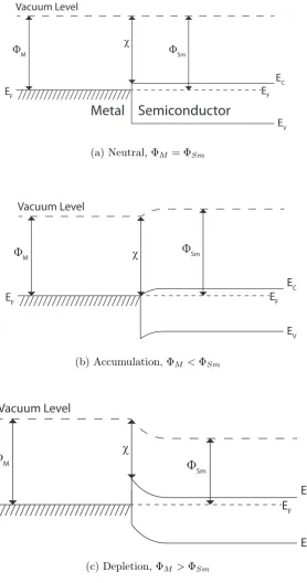
the barrier height and tunnelling resistance. . . 10
1.5 The three possible band structures of a metal-semiconductor
inter-face, depending on the relative values of the metal and semiconductor
work functions, ΦM and ΦSm. Thermal equilibrium forces the Fermi
levels in the two materials to be continuous across the interface. . . . 12
1.6 A more detailed diagram of a depletion contact showing the band
structure immediately prior to and after contact. . . 13
1.8 The affect of doping density on the width of the Schottky barrier. . . 15
1.9 Image force lowering of the barrier height. . . 16
1.10 The ideal IV characteristics and superconducting density of states of
a single Sm-S tunnel junction. The low temperature current is zero
forV <∆/e (V <2∆/e for a double junction), then asymptotically
approaches the room temperature value given by I =V /RT. RT is
often found in this way. At higher temperatures ambient electrons
are more likely to gain enough energy through thermal excitation to
tunnel across the junction, described by the broadening of the
Fermi-Dirac distribution. The IV curve was calculated using equation 1.10
with the parameters: ∆ = 0.2 meV (aluminium) andRT = 500 Ω. . . 18
1.11 Γ parameterises the population of sub-gap states and allows for low
energy electrons (E < EF) to escape the normal state material . . . 21
1.12 PC (black) andPe−phfor bath temperatures of 300 mK (red), 400 mK
(blue) and 500 mK (green), depicting cooling to 65 mK, 200 mK and
400 mK respectively. Calculated using equations 1.11 and 1.16. . . . 23
1.13 Lattice mismatch induced strain . . . 24
1.14 Strain relaxation through disclocation . . . 25
1.15 The affect of strain on the population of the conduction band valleys
in silicon. . . 26
1.16 An energy level diagram showing a quasiparticle trap applied to the
superconducting electrode of a single junction N-I-S. . . 30
1.17 Simulations of an S-Sm-S thermometer junction with ∆ = 0.2 meV,
Γ = 0.01 ∆ andRT = 500 Ω. . . 36
1.18 Further simulations of an S-Sm-S thermometer junction with ∆ =
0.2 meV andRT = 500 Ω. In figure 1.18b, the optimum current bias
1.19 A simulation of the electron temperature measured by a junction
thermometer biased at a current of 0.1 nA (blue), 1 nA (green), 10 nA
(magenta) and 100 nA (red), with ∆ = 0.2 meV, RT = 500 Ω and
Ω = 30 nm×20µm×10µm. The black dashed line represents the
true electron temperature, as measured by an ideal thermometer. . . 38
1.20 A simulation of the electron temperature measured by a junction
ther-mometer biased at a current of 10 nA with an electron-phonon
cou-pling constant of Σ = 1×10⁹W K−6m−3 (blue), 1×10⁸W K−6m−3
(green) and 1×10⁷W K−6m−3(red), with ∆ = 0.2 meV,RT = 500 Ω
and Ω = 30 nm×20µm×10µm. . . 39
1.21 Calibration of dummy experimental data (black circles) against
the-oretical isothermal junction behaviour from T = 0.01 mK to T =
0.40 mK as given by BCS theory. . . 40
2.1 The fabrication process for Sm-S and Sm-I-S junctions (Advise
rotat-ing head 90◦ anticlockwise). . . 44
2.2 The bi-layer process for silicon-vanadium junctions. . . 45
3.1 A simplified depiction of the two cooling phases of the Heliox AC-V
cryostat (reproduced from the Heliox Operator’s Handbook). . . 48
3.2 The PCB layouts of the Heliox AC-V’s two sample stages. . . 50
3.3 The Configuration of the shielded sample stage. When sealed, the
samples are entirely enclosed in copper save for a small outlet for the
PCB connector on the rear facing side. The two parts of the shield
are screwed together, the thread creating a meandering path for any
incident radiation. . . 51
3.4 A van der Pauw type sample set up for a measurement of (a)
3.5 A Hall bar type sample set up for a measurement of (a) resistivity
and (b) Hall effect. In base cases the current flows from the source
(S) to the drain (D). . . 54
3.6 Test structures and setups with contacts of widthZ and lengthL. . 57
3.7 A standard measurement setup of a typical cooler device. . . 58
3.8 The AC measurement circuit complete with 1 GΩ current setting
re-sistors. . . 61
3.9 A protective carbon strip is deposited over the top of the cross-section
to be excised. . . 65
3.10 The cross-section is exposed. . . 65
3.11 A U-cut is made to prepare the cross-section of extraction. . . 65
3.12 A micromanipulator is attached to the top of the cross-section, to
support it once free of the bulk material. . . 65
3.13 The release cuts are made and the cross-section is lifted out in-situ. . 65
3.14 The cross-section is then placed on and adhered to a TEM support
grid before being cut free from the micromanipulator. . . 65
3.15 The cross-section then undergoes a final stage of thinning. . . 66
3.16 The cross-section is now electron-transparent and can thus be imaged
using conventional TEM. . . 66
4.1 The efficiency of an aluminium based Sm-S cooler junction calculated
using equation 4.3 (solid line) and 4.4 (dashed line). . . 68
4.2 Plotting cooling power normalised to RT and ∆ allows for a direct
comparison of the relationship between optimum power and
temper-ature for devices incorporating either aluminium (red), platinum
4.3 A large band gap allows for a greater voltage to be applied across a
junction before it becomes over-biased. Calculated with the
parame-ters: RT = 500 Ω, Σ = 1×10⁸W K−5m−5 and Ω = 30 nm×20µm×
10µm. The band gaps of aluminium (red) and vanadium (black) are
highlighted. . . 71
4.4 Optical micrographs showing fabrication issues with vanadium devices. 71
4.5 Extracted voltage-temperature data of the cooled semiconductor
vol-ume. Each coloured data group represents a voltage sweep at a single
bath temperature, ranging from 300 mK to 2 K. . . 72
4.6 Current voltage characteristics of the silicon-vanadium cooler device
at 2 K (red) and 300 mK (blue). . . 74
4.7 The minimum electron temperature versus half band gap achieved
by a cooler junction at the optimum operational voltage in the ideal
(Γ = 0) case (blue) and non-ideal (Γ = 0.01 ∆) case (red). Calculated
with the parameters: RT = 500 Ω, Σ = 1×10⁸W K−5m−5 and Ω =
30 nm×20µm×10µm. . . 75
4.8 The efficiency is shown to decrease for higher values of ∆. Calculated
with the parameters: RT = 500 Ω, Σ = 1×10⁸W K−5m−5 and Ω =
30 nm×20µm×10µm. . . 76
4.9 The effect of a band gap width on unwanted cold electron tunnelling.
By shrinking the total number of available gap states (green) one
can reduce the fraction of junction current made up of electrons with
energy below the Fermi level EF. . . 77
4.10 Simulated response of a S-Sm-S thermometer with ∆ = 0.2 meV
(alu-minium - red) and ∆ = 0.07 meV (platinum silicide - blue), with
4.11 Broadened density of states (Γ = 0.05 ∆) calculated using the Dynes
model (equation 1.12) for ∆ = 0.2 meV (aluminium, red) and ∆ =
0.07 meV (platinum silicide, blue). . . 79
4.12 Device layout and cross-section of the PtSi cooler. The junction areas
are 2.5µm by 5µm and the implanted region has a length to width
ratio of 3, giving a series resistance RSm of 320 Ω. . . 79
4.13 Sheet resistance versus temperature, showing superconducting
tran-sition temperatureTC of PtSi for layer thicknesses of (a) 100 nm (b)
10 nm. . . 81
4.14 (a) Log current axis IV results for the 10 nm thick PtSi cooler (the
inset shows the same data with a linear current axis) (b) Differential
conductance. All figures use the same experimental data measured
at 100 mK (black circles). The red line shows the 100 mK isotherm fit
to the experimental data. The isotherm model uses the parameters
∆ = 70µeV, Γ = 0.8×10⁻²∆, R
T = 300 Ω, RSm = 320 Ω. The
solid lines (blue) use a cooling model, with additional parameters:
Σ = 3.1×10⁸W K−6m−3 and Ω = 1.41×10¹⁷m3. . . 84
4.15 Temperature-Voltage calculations for a bath temperature of 100 mK.
The red line uses the same parameters except for a larger delta (∆ =
190 meV) . . . 85
4.16 Simulations as the electron temperature is allowed to vary and the
cooling power is increased from zero in the isothermal case (black
dot-dashed) through 1% (red), 10% (green), to that calculated in the
full cooling model (blue), showing (a) the enhancement of the peak
in the differential conductance (The inset is a close-up of the peak
5.1 (left) An SEM micrograph of a carrier-phonon test structure. (right)
The original device schematic. Aluminium leads for the heating of
the bar are shown in red whilst the thermometer leads are coloured
blue. Each individual junction has an area of 16µm2. The central
green area is the highlighted mesa bar structure. . . 90
5.2 The VB = 0 points in the data (black circles) are used to calibrate
thermometer voltage against temperature. . . 91
5.3 Hole and electron coupling data. . . 93
5.4 Carrier phonon conductance for a hole (red) and electron control
(green) device. The two lower data sets are taken from measurements
carried out in Helsinki of the same electron control device (blue) and
the strained electron device (black). The open circles are the
low-est power points of the measurement. The slope of the fitted line,
indicating the exponent of the power law, is noted for each data set. 97
6.1 W6 single junction resistance wafer map. . . 101
6.2 W6 TLM device wafer map. . . 101
6.3 W7 single junction resistance wafer map. . . 102
6.4 W7 TLM device wafer map. . . 102
6.5 W8 single junction resistance wafer map. . . 102
6.6 W8 TLM device wafer map. . . 103
6.7 W9 single junction resistance wafer map. . . 103
6.8 W9 TLM device wafer map. . . 103
6.9 The wafer average contact resistance as measured for the three
dif-ferent characterisation structures. . . 104
6.10 The fit generated by the thermal model shows excellent agreement
6.11 The device layout. The single cooler junction area was 2×9µm2
and the thermometer junctions have a diameter of 1µm. The cooled
volume is given by the dimensions of the electrically active layer of
the mesa, being 10µm×25µm×150 nm = 37.5µm3. . . 108
6.12 Characteristic IV and VT plots for the semiconductor-insulator-superconductor
junction cooler junction on wafer W8. Each coloured set of data
rep-resents a complete voltage sweep at a particular bath temperature.
The bath temperature was varied between 120 mK and 400 mK in
20 mK steps. . . 110
6.13 Empirical calibration of thermometer junction voltage against
elec-tron temperature at zero cooler bias. The red line shows the
calibra-tion extrapolated from the linear region of the thermometer data. . . 111
6.14 Electron temperature Te against cooler bias VC. The red and blue
markers are experimental data showing cooling from 300 mK and
200 mK respectively. The green curves are fits generated by the
cool-ing model. Both fit lines are generated from the same set of
parame-ters, given in table 6.3. . . 111
6.15 Tmin/Tb versusTb showing cooler performance of the strained silicon
Sm-I-S cooler (triangles) over a range of temperatures. The results
from a previous generation of Sm-S cooler (circles) are included for
comparison. The solid green lines represent the minimum
tempera-ture predicted by the cooling model for each of the two samples. . . 112
6.16 Electron-phonon conductance of the W8 wafer. . . 113
6.17 The fit generated by the thermal model shows excellent agreement
7.1 The device has an array of interdigitated parallel junctions that are
used to cool the electron gas in the long thin central mesa. The
geometry both improves the quasiparticle thermalisation and reduces
the total resistance of the silicon. . . 119
7.2 Characteristic IV and VT plots for the strained
semiconductor-insulation-superconductor junction. Each coloured set of data represents a
com-plete voltage sweep at a particular bath temperature. The bath
tem-perature was varied between 200 mK and 570 mK in 10 mK steps. . . 120
7.3 Thermometer calibration. . . 121
7.4 Electron temperature Te against cooler bias VC. The red and blue
markers are experimental data showing cooling from 300 mK and
200 mK respectively. The green curves are fits generated by the
cool-ing model. Both fit lines are generated from the same set of
parame-ters, given in table 7.2. . . 122
7.5 Tmin/Tb versusTb showing cooler performance of the strained silicon
Sm-I-S cooler (triangles) over a range of temperatures. The results
from a previous generation of strained silicon Sm-S cooler (circles) are
included for comparison. The solid green lines represent the minimum
temperature predicted by the cooling model for each of the two samples.124
7.6 Tmin versusTb of the strained silicon SmIS cooler (triangles) and the
strained silicon Sm-S cooler (circles). Plotting the data on these axes
makes it clear that the coolers work to reduce the net temperature of
the electrons across a wide range of temperature, operating below the
Tb =Tmin line, and are only in danger of self-heating in the region
8.1 Lithography photomask designs showing the proposed layout of a 1D
Sm-S nano-wire cooler. The nano-wire measures 3µm in length, with
a width of 300 nm. The green highlighted section of the substrate
Abbreviations and Symbols
BCS Bardeen Cooper Schrieffer theory of superconductivity and the origin
of the superconducting band gap
β A parameter describing the fraction of power deposited in the
super-conducting electrode and that is returned to the semiconductor
∆ Superconductor half band gap
EF Fermi level/energy
Γ Quality factor given by the ratio of the normal state resistance and the
sub-gap resistance
IV Current-Voltage
NEP Noise Equivalent Power
N-I-S Normal metal - insulator - superconductor
Ω Actively cooled volume of a given device
PC Voltage dependent cooling power
Pe−ph Heating power manifested as a result of energy loss between electrons
and phonons
PJ Heating power caused by Joule heating
Popt Cooling power at an optimum bias voltage
PQP Heating power associated with quasiparticle effects
PtSi Platinum Silicide
RS Sheet resistance
RSm Resistance of semiconductor electrode
RT Normal state tunnelling resistance
Sm-I-S Semiconductor - insulator - superconductor
Σ Carrier - phonon conductance
TLM Transfer Length Method
TJC Tunnel Junction Cooler
Tb Bath temperature
TC Superconductor critical temperature
Te Electron temperature
Tmin Minimum electron temperature
VC Voltage across a cooler junction
VT Voltage across a thermometer junction
1
Introduction
1.1
The need for cryogenics
The most accurate and sensitive scientific equipment ever built operates in the
low temperature regime. Terahertz security cameras that generate and capture
imaging radiation at 10 K are now a common site in airports [1]. Cutting edge
hospital magnetoencephalography machines study the human brain with electronics
operating at 4 K [2], and the D-Wave system, hailed as the world’s first quantum
computer, is built around a chip set kept at a cool 20 mK [3].
For these systems it is not technology that limits their ability to function, but
the background noise that can obscure or destroy whatever it is they are studying.
Quantum computers for example, require the sub-kelvin environment necessary to
both read and manipulate information free from the coherence shattering chaotic
and classical effects associated with higher temperatures [4].
Low temperature environments are subsequently used in applications that
include the most powerful computers on the surface of the planet and the most
advanced satellites orbiting above it. Furthermore, a vast proportion of modern
day astronomical instruments rely on the low thermal noise of the sub-Kelvin
envi-ronment. The Background Imaging of Cosmic Extragalactic Polarization (BICEP)
utilis-ing a temperature of∼300 mK to garner increasingly detailed images of the cosmic
microwave background (CMB). Similarly, on board the Planck space observatory
[7], ultra-sensitive radiation detectors cooled to 100 mK continuously scan the CMB
for anisotropies and structures in the after effects of the big bang, hoping to shed
light on the begins of the universe.
Unfortunately, operating at these temperatures can prove to be very difficult
and perhaps more importantly, prohibitively expensive.
Currently, such temperatures are reached through conventional cryogenic
systems that consume 3He, utilising its low boiling point [8]. This element is in
increasingly short supply, is difficult to store and transport, and its use limits the
operational lifetime of remote cryostat systems which will eventually run dry.
Fur-thermore, for non-terrestrial experiments and applications that require a sub-Kelvin
sensing environment, the difficulty and monetary cost of carrying a liquid helium
supply into orbit presents a serious impediment.
Tunnel junction coolers (TJCs) [9, 10] form part of a relatively young area of
cryogenics that has generated a great deal of interest in its short life. Through the
use of an energy selective tunnel junction the effective temperature of an electron
population in a conducting material can be lowered. This cooling can in turn be
used to reduce the temperature of thermally contacted bulk material [11], allowing
for cryogen free refrigeration. The cooling power associated with TJCs is typically
of the order of picowatts (10−12W) [12], implying that their operational range is
limited to sub-Kelvin temperatures where the heat load is sufficiently low so as to be
overcome. Established closed cycle cooling methods, such as pulse tube refrigerators
(section 3.1.1) and adsorption pumps (section 3.1.2) are capable of handling cooling
from 300 K to 3 K and 3 K to 0.3 K respectively, therefore combing these technologies
would allow TJCs to form the final stage of a compact, all electrical/dry cooling
route from room temperature down to 0.01 K. Additionally, with reports of TJCs
the adsorption stage altogether, leading to simpler cryostat operation and a further
conservation of cryogenic material.
Such cryogen-free systems could see the application of low noise environments
to entirely new projects, domestic, laboratory and otherwise, that would previously
have been impossible due to the high cost and large volumes imposed by conventional
cryogenics.
Furthermore, TJCs have more direct applications to the fields of bolometry
and remote sensing in which the cooled electrons themselves form part of a detector
circuit with the high signal to noise ratio afforded by low temperature operation.
The absence of moving parts and subsequent vibrations is also a major benefit to
this field of applications.
To summarise, with TJCs forming part of a self-contained, low running cost
cooling system, existing cryogenics can become cheaper and more accessible, having
a significant impact on the worlds of astronomy, computing and medicine in which
low temperature sensing is key.
1.2
Thermoelectric cooling and the alternatives
Thermoelectric cooling has been an active field of research since the discovery of
the thermoelectricity by T. J. Seebeck in 1821 [14]. The Seebeck effect describes
the generation of an electric current through a junction formed of two different
conductors in the presence of a thermal gradient. When this process is reversed, a
current flowing through the junction will establish a temperature difference between
the two sides in a process known as the Peltier effect [15].
The Peltier effect can be explained as follows. When a junction is formed from
two materials with differing electrical conductivity there will exist a voltage between
them, known as the contact potential. Depending on the sign of this potential,
resulting in local cooling or heating at the material interface.
Utilising this method, Peltier coolers are capable of maintaining a
temper-ature difference across a device of around 70 K at room tempertemper-ature [16], though
they are limited by the size and thermal conductivity of their component materials,
with performance dropping to only a few degrees at 77 K [17], making them rather
unsuitable for modern cryogenic applications.
Adiabatic demagnetization refrigerators (ADRs) were the next step in
cryo-genic technology and were first successfully demonstrated in 1933 [18]. They operate
through the application of large magnetic fields (of the order of several tesla [19]) to
an electromagnetic spin system. The spins orientate themselves with the magnetic
field and when this field is removed, the spins relax into a random distribution,
ab-sorbing thermal energy in order to perform their reorientation. ADRs can typically
access temperatures of the order of 100 mK, with systems utilising the spins of
para-magnetic salts reaching 38 mK [20]. Furthermore, special types of ADRs known as
an NDRs or a nuclear demagnetization refrigerators work with the magnetic dipoles
of atomic nuclei rather than electrons, and have been demonstrated to cool a solid
to temperatures as low as 2µK [21].
Unfortunately, ADRs and NDRs suffer from a number of drawbacks. The
high magnetic fields require superconducting magnets, which require a large amount
of power to operate and must be constantly cooled below their transition
temper-ature. Additionally, Adiabatic demagnetization is a ‘one shot’ method, in that the
cooling power of the system is delivered in one temporary burst when the
mag-netic field is disengaged and the spins disorient. Once the minimum temperature
is achieved, the system will begin to warm, and the magnetization cycle must be
repeated. This naturally limits its use to short time-scale applications.
Dilution refrigerators were developed in order to solve this issue. They
op-erate using a mixture of 3He and 4He and are capable of continuous operation at
operational principles of dilution refrigerators are explained in detail in section 3.1.3.
Whilst it is possible to cool further via this method, practical limitation come
into play. Chiefly, dilution refrigerators require a large amount of power and their
base temperature exponentially proportional to the volume of the helium mixing
chamber, leading to impractically large designs [23, 24].
1.3
Tunnel junction coolers
Tunnel junction coolers stand apart from the preceding cryogenic technology,
offer-ing sub-Kelvin temperatures without any of the movoffer-ing parts, cryogens, magnetic
fields or high power requirements of the competition. They instead operate on the
principle of direct electron cooling. Similar in concept to the ‘Maxwell’s demon’
thought experiment [25], the technique utilises an energy dependent filter to
selec-tively remove electrons with an energy greater than the population average, denoted
by the Fermi levelEF N. This leads to a sharpening of the Fermi distribution and the
remaining electrons can be said to have been cooled. This method was pioneered
in the normal metal - insulator - superconductor (N-I-S) junction [26, 27] which
utilises the band gap of a superconductor as the energy filter.
1.3.1 The superconducting band gap
Superconductivity was first formally explained Bardeen, Cooper and Schrieffer in
the well known theory that bears their names (BCS) [28]. It details the formation
of a band gap in superconducting materials, a range of energy within which the
electron density of states is zero. In other words, superconductors are capable of
discriminating between electrons of certain energies, conducting some and blocking
others.
TC according to the expression
∆0= 1.764kbTC, (1.1)
common to all superconducting materials, where ∆0 is the energy gap at a
temper-ature of 0 K.
BCS theory also predicts how the band gap will change with the temperature
of the superconductor, with ∆ = 0 at TC, the point at which superconductivity is
extinguished. This relationship is derived in references [29] and [28] and is shown in
figure 1.1.
0 0.2 0.4 0.6 0.8 1
0 0.2 0.4 0.6 0.8 1
T/T C
∆
(T)/
[image:33.595.180.463.319.544.2]∆ 0
Figure 1.1: Variation of band gap with temperature.
It is immediately apparent that providingT <0.4TC, the band gap is
approx-imately equal to its zero temperature magnitude. Given that the results presented
within this thesis are drawn from experiments carried out well below this limit, it
should be noted that within this investigation the temperature dependance of ∆ is
largely ignored, with ∆ = ∆0 assumed throughout.
it is possible to design and operate devices that take advantage of their selectivity.
1.3.2 Normal metal - insulator - superconductor junctions
An energy diagram of a normal metal - insulator - superconductor junction is
pre-sented in figure 1.2 and shows the energy distribution of the electrons in the normal
metal relative to the band energies of the superconductor (with a half-band gap of
∆). The metal and superconductor are separated by a thin insulating tunnel barrier
which breaks thermal equilibrium and enables a bias voltage to be applied across
the two electron subsystems.
∆
∆
E
FS
E
FN
S
N
I
(a) Unbiased.
∆
∆
E
FS
E
FN
eV
CS
N
I
(b) Biased at an optimum voltage of VC = ∆/e, with each tunnelling electron removing an energyE−eV from the metal side, where
eis the charge of a single electron.
Figure 1.2: An energy level diagram of an N-I-S junction with and without an applied bias.
For temperatureskBT ≪∆, all states below the band gap in the
supercon-ductor will be occupied, whilst all states above will be empty. If the junction is
unbiased, as is the case in figure 1.2a, there is no electron transfer across due to the
energy inequality between the electrons in the metal and the available (unoccupied)
states in the superconductor. If, however, a voltage bias is applied so as to lift the
electrons with energy E > EF N will be preferentially removed from the metal, as
shown in figure 1.2b. This ability to filter ‘hot’ electrons is lost if the junction is
biased beyond the energy gap, at voltages greater than VC = ∆/e, illustrated in
figure 1.3. The junction is therefore said to be optimally biased at VC = ∆/e, at
which point the electron temperature will minimize.
∆
∆
E
FS
E
FN
eV
CS
N
I
Figure 1.3: When the Fermi level in the metal is biased above the superconducting
band edge both ‘hot’ and ‘cold’ electrons (with energyE < EF N) are able to tunnel
out. This removes the cooling effect and leads to heating in the device due to the uncompensated ohmic heating (see section 1.4.6).
1.3.3 Semiconductor - superconductor junctions
Semiconductor - superconductor (Sm-S) junctions were developed as an alternative
to N-I-S devises, replacing the normal metal with a highly doped semiconductor [31].
A moderately doped semiconductor (with a dopant concentration below 1018cm−3
in the case of silicon [32]) contains individual impurities that act as localized states,
donating carriers by thermionic emission or phonon-assisted tunnelling. At higher
doping concentrations these localized states can be treated as a continuous impurity
band and the semiconductor will act as a conductor with a temperature independent
resistance, though possessing far fewer charge carriers than a true metal. Such a
In principle, the reduced electron density in semiconductors makes it easier
to reach lower electron temperatures given that less entropy has to be extracted
from the system, however, this limits their ability to cool a thermally connected
load and makes them less suitable to cooling bulk material [11].
The Schottky tunnel barrier that forms between a degenerate semiconductor
and a superconductor ([32], [33], [34]) is employed in the same role as the insulating
layer in an N-I-S device, forming an energy-selective tunnel junction with the
su-perconductor. The automatic formation of the barrier simplifies device fabrication
and allows for the tunnelling probability (and hence the resistance of the junction)
to be tuned by controlling the doping density. These advantages over the N-I-S
designs are coupled with a greater robustness and reliability [35] as well as industry
compatible, high yield micromachining techniques.
Sm-S devices do however suffer from some drawbacks, most notably the fact
that even highly doped semiconductors have a higher resistivity than metals (due,
at least in part, to the smaller density of states at the Fermi level) and it is of the
order of (10−100) kΩµm2 as compared to (1−2) kΩµm2 [11] or 0.3 kΩµm2 [36] for
metal coolers. The tunnel resistance across the Schottky barrier of an Sm-S junction
is therefore, in general, higher than the tunnel resistance across the insulator used
in a N-I-S junction. This is currently a major factor in limiting device performance.
1.3.4 Double junctions
In practice, two junctions are often used in series in a symmetric configuration, as
shown in figure 1.4. The second junction assists in the cooling of the system by
enabling electrons with energy below the Fermi level to replace the more energetic
electrons that are removed by the first junction. Furthermore, this serves to prevent
charge build up within the device. Within this investigation, all devices utilize such
a double junction geometry, with an optimum operational voltage ofVC = 2∆/e, or
Schottky
barriers I
C
∆
∆
∆
∆ E
F
E F S
[image:37.595.212.429.104.305.2]S Sm
Figure 1.4: An energy level diagram of an S-Sm-S junction depicting the energy distribution of electrons in the conduction band of the semiconductor and the con-duction and valence bands of the superconductor. Although the Schottky barrier is not susceptible to the same defects as an oxide layer, impurities and surface imper-fections will still affect the barrier height and tunnelling resistance.
1.4
Tunnel junction theory
1.4.1 Metal-semiconductor contacts
To understand the operating principle of a semiconductor-superconductor tunnel
junction cooler it is necessary to first understand the nature of the interface between
a metal and a semiconductor (as summarised in Rhoderick [34], Schroder [33] and
Sze [32]).
The work function of a solid Φ is defined as the difference in energy between
the vacuum level (the energy of a free electron in vacuum) and the Fermi level, or in
other words, the energy required to free an electron with energyEF from a material.
The electron affinityχof a semiconductor is defined as the energy difference between
the vacuum level and the conduction band edge. The requirement for both the
vacuum level and the Fermi level to be continuous across the metal-semiconductor
can be expressed as the difference between the metal work function ΦM and the
electron affinity, as shown in figure 1.5.
ΦB= ΦM −χ. (1.2)
This is known as a Schottky barrier and according to equation 1.2, its height
is independent of the doping density in the semiconductor and any of the three types
of barrier shown in figure 1.5 can be implemented simply by choosing a metal with
the appropriate work function.
In reality, barrier heights and types determined by experiments [37] exhibit
only a weak dependence on the work function of the metal, with a depletion type
contact forming in almost all cases. Figure 1.6 shows a depletion contact to n-type
silicon, which proves to be the most relevant case to this investigation.
As indicated by figure 1.6a, at the moment of contact electrons will pass from
the semiconductor into the metal and the Fermi levels will align. The excess negative
charge on the metal side of the interface is balance by the now uncompensated donor
ions in the electron depleted region of the semiconductor. These donor atoms, which
occupy a width w, proportional to the difference in the semiconductor and metal
work functions, give rise to a uniform space charge and an electrostatic potential
that increases quadratically towards the interface (∝ w2), resulting in the barrier
depicted in figure 1.6b.
The apparent insensitivity of barrier height to work function is often
at-tributed to a phenomenon known as Fermi level pinning. In broad terms, this
involves the Fermi level in the semiconductor being pinned at some energy in the
band gap as a result of states present at the interface between the semiconductor
and the metal. It has been suggested that these states may be dangling bonds [38]
and that their density can be affected by preparation of the semiconductor surface
ΦM
E
F EF
E V ΦSm
Vacuum Level
χ
E C
Metal
Semiconductor
(a) Neutral, ΦM = ΦSm
ΦM
E F
Vacuum Level
E F
E V E
C ΦSm
χ
(b) Accumulation, ΦM <ΦSm
Φ
ME
F EF
E
V
E
C
Φ
SmVacuum Level
χ
[image:39.595.186.465.114.643.2](c) Depletion, ΦM >ΦSm
Figure 1.5: The three possible band structures of a metal-semiconductor interface, depending on the relative values of the metal and semiconductor work functions,
ΦM and ΦSm. Thermal equilibrium forces the Fermi levels in the two materials to
Vacuum Level
Φ
M
χ Φ
S
E
F
E
F
E
V
E
C
Φ
M- χ
(a) Prior to contact.
ΦM
E F
ΦB
Vacuum Level
E F
E V E
C ΦSm χ
w
[image:40.595.187.467.120.418.2](b) In contact, with open (shaded) circles representing uncompen-sated (compenuncompen-sated) donors.
Figure 1.6: A more detailed diagram of a depletion contact showing the band struc-ture immediately prior to and after contact.
by imagining a constant distribution of states at the metal-semiconductor interface,
centered around a neutral levelϕ0 as shown in figure 1.7.
Conservation of charge across the junction requires that
QM +QD+QSS = 0 (1.3)
withQM being the negative charge on the metal surface,QD representing the
pos-itive charge due to the uncompensated donors in the semiconductor andQSS being
the charge due to surface/interface states.
fo-EF EF Φ0
Donor-like
Acceptor-like E
C
EV
(a) Initial barrier height expected when ignor-ing interface states.
EF EF Φ0
EC
EV ,
(b) Pinning and its affect on the Schottky barrier height.
Figure 1.7: Energy level diagrams showing the effect of the neutral level and the Fermi level being pinned together. Ocupied states (circles) are shaded.
cus on the case whereϕ0 is below EF, the surface states will contain a net negative
charge. According to equation 1.3,QD must then be larger than it would be should
the surface states be absent, implying a greater number of uncompensated donors.
This results in an increase in the depletion width w along with a corresponding
increase in the band bending and subsequently the barrier height, which (as
men-tioned earlier) is ∝w2. Figure 1.7illustrates how the rise in ΦB shifts the neutral
level upwards, narrowing the gap between the neutral level andEF and reducing the
effective negative charge of the interface. It can therefore be seen that the surface
states behave as a negative feedback loop, driving the Fermi level towards ϕ0 and
pinning it to the middle of the metal-semiconductor interface, effectively precluding
the barrier types shown in figure 1.5a and 1.5b.
Clearly, this presents a problem when attempting to fabricate low resistance
metal-semiconductor contacts for device purposes. Whilst electrons can be
ther-mally excited across the Schottky barrier, these excitations become negligible at the
low operational temperature relevant to this investigation. It is therefore desirable
to modify the Schottky barrier in order to boost the probability of an electron being
able to tunnel through quantum mechanically.
engineer-Φ
Bw
Φ
Bw
Increased doping density
Figure 1.8: The affect of doping density on the width of the Schottky barrier.
ing, it is necessary instead to reduce the barrier width which can be achieved by
raising the doping concentrationND of the semiconductor, thus increasing the
uni-form space charge on the semiconductor side of the contact [34]. This enables the
accumulation of negative charge on the metal side to be balanced out by a shorter
depletion region, producing a narrower barrier as illustrated by figure 1.8.
Furthermore, increased doping concentration will in fact lower the height of
the Schottky barrier as a result of what is known as the image force [33]. Due to
the fact that the electric field must be perpendicular to the metal surface, one can
treat the situation of an electron approaching the barrier as that of approaching a
positive charge in the position of its own reflection. This adds an ‘image potential’
of the familiar 1/r2 form to that of the Schottky barrier which results in a slight
decrease in its magnitude (∝ND1/4 [34]), depicted in figure 1.9
For high doping concentrations the Schottky barrier can become narrow
enough at the base of the conduction band to allow for the direct tunnelling of
electrons between the metal and the semiconductor (i.e. field emission rather than
thermionic emission) and the contact can be thought of as ohmic, with a
Metal Semiconductor
-
+
-Surface charge Image charge
Electron
(a) Surface charge and image charge equivalence.
E
FE
FE
CSchottky potential Image potential
Barrier
(b) The addition of the two potentials and the resulting barrier.
Figure 1.9: Image force lowering of the barrier height.
1.4.2 Tunnel current
At temperatures below 1 K the thermal coupling between an electron gas and its
associated crystal lattice can weaken [41], with the electron-phonon interaction rate
dropping below the electron-electron iteration rate [42]. In other words, the internal
relaxation rate of the electron system is faster than any external couplings. This
allows the electrons to maintain a quasi-equilibrium, their energy described by the
Fermi-Dirac thermal distribution with a well defined effective electron temperature.
temperature below that of the lattice with only a moderate cooling power.
This cooling power arises from the current of electrons with energy greater
thanEF leaving the semiconductor, each removing an energy E−eV [26, 43, 44].
This current is given by [26, 45, 46, 36]
I = 1
eRT
∫ ∞
−∞F(E, V, Te, Tb).g(E)dE (1.4)
with
F =f(E−eV, Te)−f(E, Tb), (1.5)
wheref is the Fermi-Dirac distribution function of electrons
f(E, T) = 1
expE/kbT + 1. (1.6)
This current is illustrated in figure 1.10a.
HereRT is the tunnelling resistance across the Schottky barrier at the
semiconductor-superconductor interface, Te is the electron temperature in the semiconductor and
Tb is the temperature of the superconductor, assumed to be equal to the
tempera-ture of the thermal bath. g(E) is the density of states within the superconductor
(see figure 1.10b) into which the electrons tunnel and can be written as [47, 46]
g(E) =
0 ∀|E|<∆
|E|
√
E2−∆2 otherwise
1.4.3 Cooling power
The current removes energy from the semiconductor at a rate [36]
PC =
1
e2R T
∫ ∞
−2 −1 0 1 2 −0.75 −0.5 −0.25 0 0.25 0.5 0.75
Voltage (∆/e)
Curr
e
nt (
µ
A)
(a) Characteristic junction IV at 5 K (red), 1 K (green) and 0.1 K (blue)
−1 0 1
0 1 2 3 4 5
Energy (Δ)
Density of states (arb.)
(b) Superconductor density of states
Figure 1.10: The ideal IV characteristics and superconducting density of states of a
single Sm-S tunnel junction [12]. The low temperature current is zero forV <∆/e
(V < 2∆/e for a double junction), then asymptotically approaches the room
tem-perature value given by I = V /RT. RT is often found in this way. At higher
temperatures ambient electrons are more likely to gain enough energy through ther-mal excitation to tunnel across the junction, described by the broadening of the Fermi-Dirac distribution. The IV curve was calculated using equation 1.10 with the
parameters: ∆ = 0.2 meV (aluminium) and RT = 500 Ω.
In the low temperature limit (T ≤∆kB), this cooling power can be approximated
by an analytical function [48] that maximizes at
Popt ≈
∆2
e2R T
[
0.59
(
kBTe
∆
3/2)
− √
2πkBTb
∆ ×exp
( − ∆
kBTb )]
. (1.8)
There exist alternative analytical expressions for this optimum power [36, 49, 44],
however these are only valid in the situations where (∆−eV)/kBTe>>1 or ∆ =eV,
neither of which apply in the more relevant case described above.
The associated optimum tunnel current can also be written as
Iopt≈0.48 (∆/eRT) √
kBTe/∆. (1.9)
For a full derivation of equations 1.8 and 1.9, I refer the reader to the work of D. V.
As mentioned in section 1.3.4, two junctions are often employed in series,
doubling the cooling power and dividing the applied voltage between the two
junc-tions equally. This results in equajunc-tions 1.4 and 1.7 becoming [44, 9]
I = 1
eRT
∫ ∞
−∞F(E, V /2, Te, Tb).g(E)dE (1.10)
and
PC =
2
e2R T
∫ ∞
−∞(E−eV /2).F(E, V /2, Te, Tb).g(E)dE (1.11)
respectfully. It is clear from equation 1.11 that the cooling power has a strong
dependence on the tunnelling resistance of the junction.
The current flow across the junction also gives rise to a number of
heat-ing mechanisms that limit electron coolheat-ing. Experimental investigations into Sm-S
junctions have attributed these performance degrading powers to states in the
su-perconductor band gap [51, 9], nonequilibrium effects [51], and quasiparticle
back-tunnelling from the superconductor[52, 53]. What follows is a brief description of
each of these mechanisms.
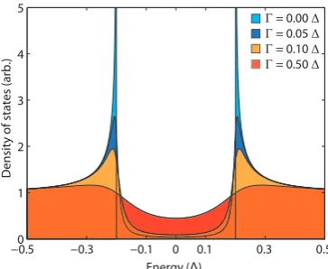
1.4.4 Sub-gap leakage and the Dynes parameter
Early experiments with Sm-S junctions [53] noted that at bias voltages below the
superconductor band gap the current flow was in excess of that described by equation
1.10. This behaviour was termed sub-gap leakage. It can be accounted for by
introducing the Dynes parameter [54] to the superconductor density of states, so
that it becomes
g(E) =Real
E−iΓ
√
(E−iΓ)2−∆2
. (1.12)
Γ modifies the superconducting density of states to allow for non-zero values within
the band gap (as shown in figure 1.11a) and effectively parameterises the availability
the superconductor material and include mechanical defects, impurities and the
proximity of the normal state material (the inverse proximity effect) [47, 9].
At low energies|E|≪∆ equation 1.12 equals Γ/∆, as shown in figure 1.11a.
Combining this with the result of Pekola et al. [55], who demonstrate that in the
low temperature limit the current through an Sm-S junction is given by
I = 1
eRT
∫ eV
0
g(E)dE (1.13)
and that the differential conductance is
dI
dV =
g(E)
RT
, (1.14)
one is left with the equation
dI
dV =
Γ
RT∆
. (1.15)
The value of Γ/∆ can therefore be determined experimentally by the ratio
of the normal state resistance RT and the sub-gap resistance, where the sub-gap
resistance is defined as dVdI(V = 0), satisfying the low energy condition mentioned
above.
Typical values of Γ are of the order∼1×10⁻⁵∆ [55] and ∼1×10⁻²∆ [56]
for N-I-S and Sm-S junctions respectively.
A non-zero value of Γ enables electrons below the threshold energy of (E−eV)
to tunnel out of the semiconductor (figure 1.11b), reducing the average energy
re-moved from the system per electron which represents a loss of filtration and
man-ifests as a net heating power. This effect becomes more prominent at low bath
temperatures, when the sharpened Fermi-distribution favours sub-gap tunneling.
It has recently been demonstrated that a Dynes-like density of states can in
fact originate from the electromagnetic environment of a tunnel junction [55]. In
Density of states (arb.)
−0.50 −0.3 −0.1 0 0.1 0.3 0.5
1 2 3 4 5
Г = 0.00 Δ Г = 0.05 Δ Г = 0.10 Δ Г = 0.50 Δ
Energy (Δ)
(a) Density of states as given by the Dynes for-mula for ∆ = 0.2 meV
Energy gap Empty states
Occupied States EF
S N I
[image:48.595.130.312.116.265.2](b) Energy level diagram of an N-I-S device with available states in the bandgap
Figure 1.11: Γ parameterises the population of sub-gap states and allows for low
energy electrons (E < EF) to escape the normal state material
from the surrounding high temperature environment, leading to the photon-assisted
tunnelling of sub-gap electrons. Once again this results in a loss of effective cooling
power, however it may be solved by simply improving the shielding on the sample
stage.
It is worth noting that in this investigation a number of samples were used for
benchmark measurements in separate cryostats with varying experimental setups,
each providing a different noise environment. In each case, the value of Γ measured
was of the same order of magnitude indicating that it is intrinsic to our devices
and therefore the result of some material property and not of the measurement
environment.
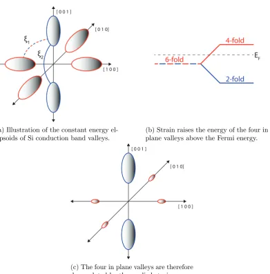
1.4.5 Carrier-phonon coupling
Electron-phonon coupling results in a power flow from the lattice to the electron gas
as the former is cooled. It can be interpreted as either a drain on the cooling power
of a junction, or an opposing heating power.
sys-tems, the coupling, although conceptually simple, is generally not possible to
cal-culate directly and approximations are needed. The most used one, is the so-called
deformation potential theorem [57], the application of which is described thoroughly
in previous work [42]. Other works have focused on the role of valley degeneracy
in phonon coupling, though a detailed theoretical analysis for the
carrier-phonon or coupling in strongly disordered, many-valley semiconductors has only
recently started to develop [58, 59, 60, 61, 62]. This theory will be touched upon in
more detail in chapter 5.
At low temperatures this energy transfer is mediated by the electron-acoustic
phonon interaction given by [41, 21]
Pe−ph= ΣΩ(Ten−Tpn) (1.16)
with Σ being the material specific electron-phonon coupling constant and Ω the
cooled volume. The power n varies with material [58] with n = 6 being typical
for degenerately doped 3D bulk semiconductors [53, 58, 60]. One advantage of
Sm-S junctions is that Σ is generally lower in semiconductors compared with normal
metals [31]. Furthermore, Σ can be tuned by doping concentration [59], carrier type
(see chapter 5) and tensile strain [63]. The latter two factors form an important
part of my investigations in this thesis, with further discussion of the power law and
its exponent value given in chapter 5.
In the simplest case, the temperature to which the electrons are cooled may
be determined by balancing the cooling power (equation 1.11) and the power drain
due to electron phonon coupling (equation 1.16) and solving the following equation
forTe.
PC+Pe−ph= 0 (1.17)
Figure 1.12 depicts this equation graphically for a range of bath temperatures (equal
in-dicated by the intersection of thePC and Pe−ph lines.
0 100 200 300 400 500
0 2 4 6 8 10
Electron Temperature (mK)
[image:50.595.176.453.149.369.2]Power (pW)
Figure 1.12: PC (black) and Pe−ph for bath temperatures of 300 mK (red), 400 mK
(blue) and 500 mK (green), depicting cooling to 65 mK, 200 mK and 400 mK
respec-tively. Calculated using equations 1.11 and 1.16 with the parameters: ∆ = 0.2 meV
(aluminium),RT = 500 Ω, Σ = 1×10⁸W K−6m−3 and Ω = 30 nm×20µm×10µm.
However, it is found in practice that this simple equation overestimates the
cooling performance for a given set of parameters and therefore other factors must
be considered that limit the electron cooling (see section 1.4.6 onwards).
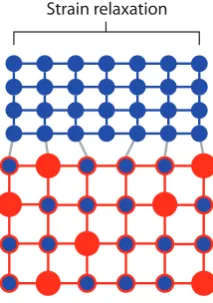
1.4.5.1 Modification through strain
Mechanical strain can be induced by growing silicon atop a substrate with a different
lattice parameter, with the silicon conforming to the atomic spacing of the material
beneath. In this and other work [63], a silicon germanium virtual substrate is used
to induce biaxial tensile strain in the overlaid silicon as depicted in figure 1.13.