A Simplified Space Vector Modulation Algorithm
for Four-Leg NPC Converters
Felix Rojas, Roberto Cardenas,
IEEE Senior Member,
Ralph Kennel,
IEEE Senior Member,
Jon Clare,
IEEE
Senior Member,
and Matias Diaz,
IEEE Student Member
Abstract—To interface generation sources and loads to four-wire distribution networks is important to use power converters and modulation methods which provide high performance, flexi-bility and reliaflexi-bility. To achieve these goals, this paper proposes a simple and efficient Space Vector Modulation (SVM) algorithm inαβγcoordinates for Neutral Point Clamped (NPC) converters. The proposed SVM method reduces a three-dimensional (αβγ) search of the modulating vectors into a simple two-dimensional (αβ) problem. Moreover, the algorithm provides full utilisation of the dc-link voltage, full utilisation of the redundant vectors and it can be applied to any other four-leg converter topology. The proposed SVM has been successfully validated using a 6kW three-level four-leg NPC converter, achieving control over the voltages of the dc-link capacitors and simple definition of switching pattern for shaping frequency spectrum.
Index Terms—NPC converters, four-leg converters, Space vec-tor Modulation (SVM), Distributed Power Generation Systems (DPGS), Unbalanced Distribution Systems.
I. INTRODUCTION
D
Uring the last decades, the Neutral Point Clamped (NPC) converter has played an important role in the integra-tion of renewable energy sources into the electrical system [1]. NPC- based commercial solutions to interface relatively large Wind Energy Conversion Systems to medium voltage transmission lines are already available in the market [2]– [4]. The utilisation of NPC converters in micro-grids and low voltage distribution systems has also been reported [5]. In this sort of applications the advantages of the NPC converters are mainly the high effective switching frequency, allowing a noticeable reduction in the filter size, and the high overall efficiency which is important in some applications, e.g to interface photo voltaic (PV) energy to domiciliary and power plants applications [4], [6].In four-leg low voltage distribution networks, a path for the circulation of zero sequence current is mandatory for
This work was supported by BMBF Germany Grant Nr. 01DN13018 and Fondecyt Chile, Grant Nr. 1140337. The support of the Basal Project FB0008 is also kindly acknowledged.
F´elix Rojas is with the Electrical Engineering Department, University of Santiago of Chile, Avenida Ecuador N 3519, Estacion Central, Santiago (email [email protected]).
Ralph Kennel is with the Institute for Electrical Drive Systems and Power Electronics, Technical University of Munich, Arcisstr. 21, 80333, Munich (email [email protected]).
Roberto C´ardenas and Mat´ıas D´ıaz are with the Electrical Engineering Department, University of Chile, Avenida Tupper 2007, Santiago, Chile (email [email protected], [email protected]).
Jon Clare is with the Department of Electrical and Electronic Engineering, University of Nottingham, Nottingham University Park, Nottingham, NG7, 2RD, (email [email protected]).
the connection of linear and non-linear single-phase loads [7], [8]. There are several well- established methods reported in the literature to provide a fourth wire for the circulation of zero sequence current. For instance, a (bulky) delta-wye transformer for providing a neutral wire from the neutral point of the secondary side of the transformer. Another solution is to provide a fourth wire connection using the middle point of a split dc-link capacitor. However, as reported in [8], this method usually produces a less efficient utilisation of the dc-link voltage and higher ripple in the dc-link capacitors. Probably the best arrangement to provide a path for the circulation of zero sequence currents is adding an extra leg in the power converter [7]. This solution provides control over the zero sequence signals and provides full utilization of the dc-link voltage.
The application of two-level four-leg converters [9], [10], and four-leg matrix converters [11]–[13] to four-wire dis-tribution networks, have been extensively reported and are considered good alternatives for connecting Distributed Power Generation Systems (DPGs) to low voltage grids. However, when high efficiency is desirable combined with high effective switching frequency (for small-size power filter), four-leg NPC converters are better alternatives [14]. Moreover, the capability of synthesising high fundamental frequencies with low distortion is also desirable in some four-wire applications, as for instance in the aerospace industry where fundamental signals above 400 Hzare required [12], [15]. Considering all the aforementioned issues, four-leg multilevel converters, such as the four-leg NPC converter shown in Fig. 1, are attractive solutions [14], [16], [17].
ia
ib
ic
if
¯
S2c ¯
S1c
¯
S2b ¯
S1b
¯
S2a ¯
S1a
S1c
S2c
S1b
S2b
S1a
S2a
iP
iC1
C1
vC1(t)
vC2(t) C2
iC2
iN
z iz
S1f
S2f
¯
S2f ¯
S1f
a b c f
2vdc +
-P
[image:1.612.309.547.567.695.2]N
Fig. 1. Electrical diagram for a four-leg Neutral-Point-Clamped Inverter
in-stance, in [14] non-linear controllers, such as Finite-Set Model Predictive Control (FS-MPC), are proposed. Unfortunately, the variability of the switching frequency is an important drawback of this approach. The use of Carrier-Based Pulse Width Modulation (PWM) applied independently to each leg of the converter has been addressed in [18]. These methods are easy to implement. However, they do not allow selection and building of vector switching patterns, which are usually required to modify the shape of the harmonic spectrum or to reduce the switching power losses. Furthermore, carrier-based PWM methods do not allow the use of vector redundancies to control the voltage imbalance in the NPC dc-link capac-itors, important issue when operation with a low switching frequency is required [19], [20].
A three-dimensional algorithm inabccoordinates have been proposed in [21]. This algorithm makes full utilization of the dc-link voltage and can modulate a reference vector with a simple and fast algorithm. However, the representation in abc coordinates inherently limits the potential of this SVM method, as the zero sequence can not be directly controlled. For instance overmodulation algorithms, as that proposed in [22], [23]; balancing of the capacitor voltages; and even harmonic elimination, [24], [25] are complex to implement when SVMs based on abc coordinates are applied to NPC converters. On the other hand, all these features are simple to implement with the SVM proposed in this work.
In this paper, a simplified and low-computational-burden SVM algorithm for three-level four-leg NPC converters is pre-sented. The simplicity of the method is based on transforming a three-dimensional search of the modulating vectors, into a much simpler 2-dimensional (αβ) problem. Moreover, the proposed SVM can be extended to any number of levels for any four-leg power converter topology.
The rest of this paper is organized as follows: In Section II the proposed modulation algorithm is discussed. In Section III experimental results, obtained with a 6kW lab prototype, are discussed and fully analysed. In Section IV an appraisal of the proposed method is introduced. Finally, in the appendix the look-up tables summarising the switching states of the converter are presented.
II. THREEDIMENSIONALSPACEVECTORMODULATION FOR AFOUR-LEGNPC INVERTER
Any space vector modulation strategy is based on the voltage-second average, where a set of voltage vectors, which represent the switching states of the converter, are used to average a reference value over one sampling time [23]. The Clarke transformation presented in (1) is used to obtain the vectorial representation of the switching combinations of the converter in anαβγ space.
Tabcαβγ = 2 3
1 −1/2 −1/2 0 √3/2 −√3/2
1/2 1/2 1/2
(1)
After the vector representation of the switching combina-tions is obtained, there are mainly three steps required to fulfil the modulation, these are described as follows: 1) To select the four-vector (tetrahedron) required to synthesise the reference
α β
γ
2
1
0
-1
-2 1.5 1
0
-1.5
1.5 1 0 -1.5
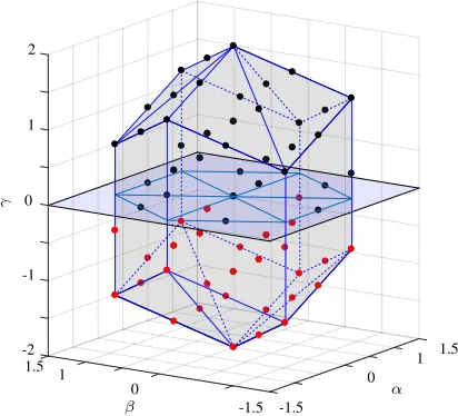
Fig. 2. Representation of the 65 different vectors in theαβγ space for a four-leg NPC converter. The external surface is also shown. Black dots are on or over theαβplane.
vector 2) To calculate the dwell time of each vector, 3) To arrange the vectors in a suitable pattern.
In the rest of this section these steps, applied to a four-leg NPC converter, are further discussed.
A. Definition of the Three-Dimensional Space of Vectors
Fig. 1 presents a four-leg NPC converter. This converter can synthesise34=81switching combinations, where(S1x, S2x)∈
{(1,1),(0,1),(0,0)} andx∈ {a, b, c, f} are the three possi-ble states for each leg of the converter. In the rest of this paper, the poles {a, b, c} are named as phases, while pole f
is referred as neutral.
To implement a SVM algorithm in αβγ coordinates, the space generated by the 81 switching combinations must be analysed. In (2), the ith switching combination of the con-verter, represented as vi
abc and defined in (3), is transformed to its αβγ representation, i.e. viαβγ with i ∈ N : [1,81]. In
(4) the instantaneous reference vector inabccoordinates, i.e.
vabc∗ , is transformed to itsαβγ representation, i.e.vαβγ∗ .
viαβγ =Tabcαβγviabc (2)
viabc= [viaf, vbfi , vicf] (3)
v∗αβγ =T αβγ abc v
∗
abc (4)
After applying (2) to the 81 different switching combina-tions, 65 different vectors in the αβγ space are generated as depicted in Fig. 2. The switching combinations corresponding to the vectorsviαβγ, are shown in Table IV (see Appendix A). These vectors are classified as follows: 14 redundant vec-tors, 50 non-redundant vectors and 1 zero vector with a triple redundancy. For convenience, Table IV summarizes this information with the following notation: the zero vector is represented as v0z
αβγ, v
0n αβγ or v
0p
αβγ; redundant vectors are represented as vkn
αβγ or v kp
αβγ, for k ∈ N : [1,14], where the sub-index n or p distinguishes the relative positive or negative polarity of the output voltages respect to the mid-pointz. This can be observed from the fourth and fifth row of Table IV, wherev1n
abcf=[ON N N]andv
1p
abcf=[P OOO], which
αβγ representation is for both cases v1abcp=v1n abc=[
2 3,0,
[image:2.612.337.543.57.244.2]Finally,vk
αβγ fork∈N: [15,50]represent the non-redundant vectors.
B. Tetrahedron Identification
The algorithm proposed in this work is able to identify the correct tetrahedron directly from the αβ plane (e.g. sim-ilar to SVM algorithms for three-leg converters), avoiding the search in the three-dimensional space. A reference vec-tor in abc coordinates is defined as v∗abc =[x, y, z], where
x;y;z∈R: [−2,2]. The corresponding representation inαβγ
coordinates is v∗αβγ, which is assumed inside the modulation region of Fig. 2. Considering that the transition between two adjacent vectors is equal to an unitary voltage step in one phase of the converter (e.g. vabc1p([1,0,0])↔ v15
abc([1,0,-1]) or equivalently [POOO] ↔ [PONO]), it can be concluded that each component ofv∗abc is bounded between the components of the vectors v0abc and v00abc defined in (6). These vectors can be obtained applying thefloor()function, (which provides the smallest integer of the argument value), to each coordinate of v∗abc:
v0abc=floor(v ∗
abc) (5)
v00
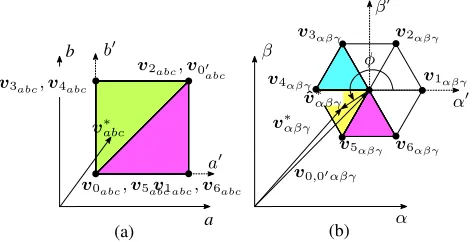
abc=v0abc + [1,1,1] (6) Thus, considering v0abc as the origin of a cube and v00abc its farthest corner, a set of six additional vectors can be defined to complete the eight corners of a cube, which are all the possible switching transitioning betweenv0abc tov00abc. These vectors are denoted asv1abc tov6abc and are shown in the first column of Table I. The complete cube in the abc space is shown in Fig. 3a with a displaced centre, positioned atv0abc. Applying (2) to the first column of Table I, the representation in αβγ
coordinates is obtained (see the second column of Table I). The vectors in αβγcoordinates are depicted in Fig. 3b, where the same cube presented in Fig. 3a has been rotated. By inspecting the vectors of Fig. 3b, it is concluded that only v0αβγ and
v00
αβγ have identical αβ components. Any other vector is completely identified using only their αβ coordinates. This is further discussed using Fig. 4.
v0abc
v5abc
v1abc
v2abc
v3abc
v00abc
v4abc
v6abc
v00αβγ
v0αβγ
v5αβγ
v6αβγ
v4αβγ
v3αβγ
v2αβγ
v1αβγ
Tabcαβγ
(a) (b)
a0 b0 c0
[image:3.612.310.546.104.225.2]α0 β0 γ0
Fig. 3. Three-dimensional representation of the eight transitioning vectors that form the cube in the (a)abcand (b)αβγspace respectively. The coordinate frames have been displaced to v0abc (or equivalently tov0αβγ), and are denoted asa0b0c0 andα0β0γ0respectively.
Fig. 4 represents the cubes of Fig. 3 shown in a non-displaced origin (abc or αβγ ) reference frame. Unlike the representation in the abc space shown in Fig. 4a, in the
αβγ space (see Fig. 4b) only two coordinates are required to unequivocally identify the six vectors, v1αβγ tov6αβγ, which are certainly not overlapped in the αβ plane. Therefore, as
shown in Fig. 4b, these six vectors can be used to create the typical hexagon generated by the vectors of a 2-level 3-phase voltage source inverter in theαβ -plane.
v0abc,v5abcv1abc,v6abc v2abc,v00
abc
v∗abc
b
a
v2αβγ
v1αβγ
v6αβγ v3αβγ
v4αβγ
v5αβγ
β
α v∗αβγ
v0,00αβγ ˆ v∗αβγ
φ
(a) (b)
α0 β0
a0 b0
v3abc,v4abc
Fig. 4. Top view of (a) Fig. 3a and (b) Fig. 3b in a non-displaced origin.
In this case, the simple calculation ofφ, shown in Fig. 4b, provides straightforward identification of the vectors required to synthesise the reference v∗αβγ. This effectively transforms a tetrahedron search, realised in a three-dimensional space, into a much simpler two-dimensional sector identification, avoiding three-dimensional computations. The following equa-tions summarize the three steps required for selection of the tetrahedron when the reference vector is given in abc coordinates:
v0αβγ=T
αβγ
abc floor(v ∗
abc) (7)
ˆ
v∗αβγ=v∗αβγ −v0αβγ=[ˆvα,vˆβ,vˆγ] (8)
φ=tan−1 ˆv
β
ˆ vα
(9)
Finally, based on the angle φ, the selection of the vectors required for the modulation of the reference signal, is simple to achieve by identifying the sector where theαβ projection of the reference vectorvˆ∗αβγ lies. Definingvs1
αβγ,v s2 αβγ,v
s3 αβγ andvs4
αβγ(or shortlyv s1−s4
αβγ ) as the selected stationary vectors that form the tetrahedron, Table II summarizes their selection for each of the sectors shown in Fig. 3b (notice that these sectors are similar to those used in the conventional SVM for two-level inverters).
TABLE I
VECTORS FORTETRAHEDRONSELECTION INabcANDαβγCOORDINATES
Transition vectors inabc Transition vectors inαβγ
v0abc=v s1
abc v0αβγ=v
s1 αβγ
v0abc=f loor v ∗
abc
+ [0,0,0] v0αβγ=T αβγ abc v
s1
abc+ [0,0,0]
v1abc=v0abc+ [1,0,0] v1αβγ=v0αβγ+ [ 2 3,0,
1 3]
v2abc=v0abc+ [1,1,0] v2αβγ=v0αβγ+ [ 1 3,
√ 3 3 ,
2 3]
v3abc=v0abc+ [0,1,0] v3αβγ=v0αβγ+ [− 1 3,
√ 3 3 ,
1 3]
v4abc=v0abc+ [0,1,1] v4αβγ=v0αβγ+ [− 2 3,0,
2 3]
v5abc=v0abc+ [0,0,1] v5αβγ=v0αβγ+ [− 1 3,−
√ 3 3 ,
1 3]
v6abc=v0abc+ [1,0,1] v6αβγ=v0αβγ+ [ 1 3,−
√ 3 3 ,
2 3]
v00
abc=v s4
abc=v0abc+ [1,1,1] v00
αβγ=v s4
[image:3.612.322.552.588.732.2]TABLE II
SELECTEDSEQUENCE OFVECTORS
φ vs1−s4
αβγ Sector 1:φ∈
0,π3
v0αβγ−v1αβγ−v2αβγ−v00αβγ
Sector 2:φ∈π 3,
2π 3
v0αβγ−v2αβγ−v3αβγ−v00αβγ
Sector 3:φ∈2π 3 , π
v0αβγ−v3αβγ−v4αβγ−v00αβγ
Sector 4:φ∈
π,43π
v0αβγ−v4αβγ−v5αβγ−v00αβγ
Sector 5:φ∈4π 3 ,
5π 3
v0αβγ−v5αβγ−v6αβγ−v00αβγ
Sector 6:φ∈5π 3 ,2π
v0αβγ−v6αβγ−v1αβγ−v00αβγ
Using the proposed algorithm, only the calculation ofv0αβγ is required for the identification of the four vectors used to synthesise the reference. As shown on Table I, all the vectors that form the hexagon in the αβ plane around v0αβγ (v1αβγ tov6αβγ) are obtained just by adding a constant term tov0αβγ (see second column of Table I).
C. Switching Sequence
In order to minimise the number of devices switching in each modulation period (minimum switching transition principle [7]), the vectors have to be applied in a pre-defined sequence. In this work the four selected vectors are arranged using always v0αβγ and v00αβγ as the first and last vectors of the sequence respectively (or vice-versa). For the proposed SVM algorithm the modulation sequence is similar to that used in a three-leg converter and this is shown in the second column of Table II.
In order to reduce the total harmonic distortion of the generated waveform, a mirror pattern can be implemented. Thereby, the sequence is symmetrically repeated during half of the total sampling time Ts. For instance, for sector 1 the proposed sequence is:
Sector1 :v0αβγ v1αβγ v2αβγv00αβγ v2αβγ v1αβγ v0αβγ (10)
Notice that other switching sequences can be implemented using the proposed methodology, e.g. discontinuous modula-tion for minimizing the switching frequency of the devices, other modulation patterns to reduce the output distortion [7], etc.
D. Dwell time Calculation
Once the four stationary vectors,vs1 αβγtov
s4
αβγ, are obtained using (9) and Table II, their dwell times must be calculated. Defining d1, d2, d3 andd4 as the dwell times for each of the
selected vectors vs1−s4
αβγ , and Ts as the sampling time, their normalized values can be obtained from:
d2 d3 d4
=Dn
ˆ
v∗α
ˆ
v∗β
ˆ
v∗γ
(11)
d1= 1−d2−d3−d4 (12)
where, from (8) the vectorˆv∗αβγ is equivalent to referring the vectorv∗αβγ to a newαβγplane, where the origin is located at
v0αβγ (i.e.α0β0γ0 from Fig. 4b). Using this displaced origin, the vectorsv1αβγ tov6αβγ will be placed always in the same position, forming the typical hexagon in the αβ plane of a two-level VSI (see second column of Table II). By that, six different 3x3 matricesDncan be defined to calculate the dwell times in all the space. This matrices take six different values depending on the sector defined by the angleφ(see Fig. 4b). Thereby, based on the second column of Table I, Dn can be expressed for each interval asφ∈h(n−31)π,nπ3 h:
D1=
3 2
-√
3 2 0 0 √3 0
-12 -√
3 2 1
D2=
-32 √
3
2 0
3 2
√
3
2 0
-12 -√
3 2 1
D3=
0 √3 0
-32 -√
3 2 0
1 0 1
D4=
0 -√3 0
-32 √
3
2 0
1 0 1
D5=
-32 -√
3 2 0 3
2
-√
3 2 0
-12 √
3
2 1
D6=
3 2
√
3
2 0
0 -√3 0
-12 √
3
2 1
(13) The diagram shown in Fig. 5 summarises the proposed methodology to implement a SVM algorithm in the αβγ
coordinate frame for a four-leg NPC converter. As depicted in this figure, after only two steps the required vectorsvs1−s4 αβγ are identified. Moreover, the calculation of their corresponding dwell-times,d1tod4, is simple to realise using the vectorˆv∗αβγ (see (11)-(13)).
For a real-time implementation of the proposed SVM algo-rithm, Table IV is not strictly required. However, this table is useful for other tasks, for instance to detect overmodulation, (see Fig. 2). Moreover, to add look-up tables with the infor-mation presented in Table IV represents a negligible use of memory space in any of the Digital Signal Processors (DSPs) currently used for power electronics applications.
Although in this work the proposed methodology is pre-sented and analysed for a four-leg NPC converter, the flexibil-ity of this algorithm allows a straightforward implementation in any four-wire topology.
E. Capacitors Voltage Balance
Once the four stationary vectors that enclose the reference have been selected and their dwell-times have been calculated. The redundant vector with the largest dwell-time can be used to actively balance the voltages on the dc-link capacitors
vC1(t) and vC2(t) of Fig. 1. For this, one dwell-time has to be subdivided into to two sub-dwell-times, one for each redundancy of the redundant vector. Assuming that vs4
αβγ is the redundant vector, the average current through the neutral point generated by the converter in one sampling time can be calculated as [14]:
i∗z =d1·iz1(v s1
αβγ) +d2·iz2(v s2
αβγ) +d3·iz3(v s3
αβγ)+ (14)
+λ·d4·iz4(v s4p
αβγ)−(1−λ)·d4·iz4(v s4n
((7),(8), (9))
v∗αβγ
Reference given by external Controller
Calculation ofv0αβγ;ˆv ∗ αβγ;φ:
vs4
αβγ=v0αβγ+ [0,0,1]
vs1
αβγ=v0αβγ
φ∈ 0,π3
φ∈π
3, 2π
3
φ∈2π
3, π
φ∈ π,43π
φ∈4π
3, 5π
3
φ∈5π
3 ,2π
vs2
αβγ=v1αβγ
vs3
αβγ=v2αβγ
d|=D
1vˆ∗αβγ|
vs2
αβγ=v3αβγ
vs3
αβγ=v2αβγ
d|=D
2ˆv∗αβγ|
vs2
αβγ=v3αβγ
vs3
αβγ=v4αβγ
d|=D
3vˆ∗αβγ|
vs2
αβγ=v5αβγ
vs3
αβγ=v4αβγ
d|=D
4ˆv∗αβγ|
vs2
αβγ=v5αβγ
vs3
αβγ=v6αβγ
d|=D
5∗ˆv|αβγ
vs2
αβγ=v1αβγ
vs3
αβγ=v6αβγ
d|=D
6vˆ∗αβγ|
[image:5.612.63.557.55.287.2](Sector 1) (Sector 2) (Sector 3) (Sector 4) (Sector 5) (Sector 6)
Fig. 5. General diagram for a three-dimensional SVM.d|denotes the transpose of the vectord= [d
2, d3, d4]. The dwell timed1is obtained asd1=1−
d2−d3−d4;∀φ.
where vs1−s4
αβγ are the selected stationary vectors for mod-ulating a reference value, d1, d2, d3 and d4 are the
dwell-times calculated in (11), iz1, iz2, iz3 and iz4 are the currents through the neutral-point (z of Fig. 1) generated by each of the vectors vs1−s4
αβγ ,i∗z is the required reference current, given by an external PI controller, to balance the voltages vC1 and
vc2 andλis the variable to be calculated which provides the portion of the positive and negative redundancy used in the redundant vector. Thereby, knowing λ, the sub-dwell time are simply obtained from (14) as:
d4p=λ·d4 (15)
d4n=(1−λ)·d4 (16) III. EXPERIMENTALRESULTS
The experimental rig used to validate the proposed SVM algorithm is depicted in Fig. 6. The control platform is based on a Pentium-System board (2Gb RAM host PC with a 3.2GHz Pentium processor running the RTAI Arch-Linux operating system) and a FPGA board. The FPGA board handles the signals measured by the A/D converters; imple-ments over-voltage and over-current protection; impleimple-ments the commutation dead time; and handles the control signals for the IGBTs switches which are transmitted to the power converter using optical fibres. The four-leg NPC converter is based on the semiconductor module Microsemi IGBT-APTGL60TL120T3G, 60A and 1200V. The experimental data has been acquired using a Textronix DPO 2024 Digital Phosphor Osciloscope, 200MHz, 1GS/s.
Notice that the execution time for the proposed simplified SVM algorithm is less than20µsec.
A. Modulation of Balanced and Unbalanced Voltages
In order to validate the performance of the proposed SVM algorithm, two criteria are considered. First, the converter
Control Platform Power Electronics Interface
[image:5.612.312.563.333.502.2]Oscilloscopes
Fig. 6. Complete view of a 6kW experimental rig for a four-leg NPC converter.
must be able to modulate each of the harmonic components present at the reference waveform. Secondly, the modulated waveforms must fulfil theminimum switching transition prin-ciple, generating a pulse pattern which reduces the harmonic distortion and switching losses. The results discussed in this section have been obtained applying switching patterns similar to that of (10). Additionally, the parameters of Table III have been used.
TABLE III
GENERALPARAMETERS OF THEIMPLEMENTEDSYSTEMS
Parameter Value Parameter Value
C1 3300 uF fs 6kHz
C2 3300 uF 2Vdc 270 V
balanced and symmetric references. These references posses an amplitude equal to95 %of the maximum value achievable by the modulation in the linear region.
vaf∗ =270√
30.95 cos(100πt) (17)
vbf∗ =
270
√
30.95 cos(100πt− 2π
3 ) (18)
vcf∗ =
270
√
30.95 cos(100πt+ 2π
3 ) (19)
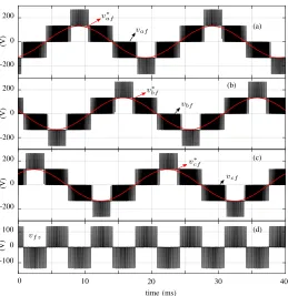
Using the algorithm described in Fig. 5, the modulation of the required voltages is achieved and depicted in Fig. 7. It can be observed that because of the fourth leg of the converter, five levels are generated at the output phase-to-neutral voltages. This increases the effective switching frequency allowing a reduction of the size of the power filters and full utilisation of the dc-link voltage. The harmonic spectrum of vaf is shown in Fig. 8 (forvbf andvcf the spectrum is equivalent). Clearly, the first group of predominant harmonics are around 6 kHz. Additionally, the fundamental component is exactly modulated with a peak magnitude of 270
√
3
3 0.95≈153.5V.
0 10 20 30 40
-200 0 200 0 200
-200 -200 0 200
time (ms)
v∗
af
v∗bf
v∗cf vaf
vbf
vcf
(V)
(V)
(V)
-100 0 100
vf z
(V)
(a)
(b)
(c)
[image:6.612.311.555.54.174.2](d)
Fig. 7. Output voltages (a)vaf, (b)vbf, (c)vcffor a four-leg NPC converter with their respective referencesvaf∗ ,v∗bfandv∗cfin red. In (d) the modulated voltage of the fourth legvf z. Sampling frequencyfs=6kHz, dc-link voltage 270V.
In Fig. 7d the modulated voltage of the fourth leg of the converter vf z is presented. As depicted in this figure, the fourth leg has to modulate a third harmonic signal in order to boost the phase-to-neutral output voltages achieving full utilisation of the dc-link voltage. From Fig. 7d (and voltages
vaz,vbz and vcz), the switching frequency of each device of the four-leg NPC converter presented in Fig. 1 can be obtained. Thereby, for each leg of the converter, the switching transitions
5 10 15
0 20 25 30 35 40
frequency kHz
Amplitude
√ 3
vaf
270
0 0.1 0.2 0.3 0.4 0.5 0.6 0.7 0.8 0.9 1.0
0.95
6kHz
12kHz
18kHz 24kHz
50Hz
Fig. 8. FFT forvaf of Fig. 7. The amplitude has been normalized by 270√ 3.
performed during the positive semi-cycle of the modulated waveform define the switching frequency of S1i (and its complementary switch S¯1i), while the switching transitions performed during the negative semi-cycle define the switching frequency of S2i (and its complementary switch S¯2i) for
i∈ {a, b, c, f}. By that, using the data provided by Fig. 7, and considering the implemented switching pattern, the switching frequency for each device of the converter are given by:
fS1a=fS1b=fS1c=fS1f=3000 Hz (20)
fS2a=fS2b=fS2c=3000 + 50=3050 Hz (21)
fS2f=3000 + 150=3150 Hz (22)
As the transition between tetrahedrons generates an extra switching commutation during the negative semi-cycle, the switching frequency of each device is not exactly3 kHz. This is noticed as an increment in50 Hz in the switches S2a,S2b andS2cand150 HzinS2f. However, this is an small quantity compared to the average switching frequency of 3 kHz, as it is always a multiple of the fundamental frequencyf1, and can
be usually negligible. Nevertheless, when the modulation is implemented for very low switching frequencies, this factor must be considered.
In order to evaluate the modulation algorithm under a general case. The following unbalanced and non-sinusoidal set of references are used for modulation
vaf∗ =270√
3 (0.9 cos(ωt) + 0.1 cos(3ωt) + 0.1 cos(5ωt)) (23)
vbf∗ =
270
√
3(0.9 cos(ωt− 2π
3 ) + 0.1 cos(5ωt+ 2π
3 )+ (24)
+ 0.15 cos(7ωt−2π
3 ))
vcf∗ =270√
3(0.8 cos(ωt+ 2π
3 ) + 0.15 cos(7ωt+ 2π
3 )+ (25)
+0.1 cos(11ωt−2π
[image:6.612.43.302.331.598.2]3 ))
[image:6.612.317.563.552.670.2]waveforms. It can be clearly noticed that each of the modulated waveforms perfectly track their harmonic references presented in (23) to (25). Additionally, Fig. 9d shows the voltage vf z, which represents the modulated voltage of the fourth leg of the converter. Unlike Fig. 7d, the voltage vf z of Fig. 9d does not represent an ideal third harmonic, but it has been modified to track each of the different harmonics in each leg of the converter. Similarly to the previous example, the switching frequency of each device of the converter can be obtained as follows
-200 0 200 0 200
-200 -200 0 200
vaf∗
vbf∗
vcf∗ vaf
vbf
vcf
(V)
(V)
(V)
0 10 20 30 40
time (ms) -100
0 100
vf z
[image:7.612.316.550.54.151.2](V)
Fig. 9. Output voltages (a) vaf, (b) vbf and (c) vcf for a four-leg NPC converter with their respective references v∗af,vbf∗ andv∗cf in red for unbalanced and non-sinusoidal references. In (d) the modulated voltage of the fourth legvf z. Sampling frequencyfs=6kHz, dc-link voltage270V.
fS1a=fS1b=fS1c=fS1f=3000Hz (26)
fS2a=fS2b=fS2c=3000 + 50=3050Hz (27)
fS2f=3000 + 150=3250 (28)
Notice that the incorporation of additional harmonics slightly modified the switching frequency compared to the previous case shown in in (20)- (22). The deviation of the switching frequency is caused by the modification of the path described by the reference vector inside the modulation region of Fig. 2. Thereby, additional commutations are incorporated when the reference vector changes from one tetrahedron to another. However, its deviation is still negligible compared to the average switching frequency defined by the switching pattern, i.e.3kHz.
B. Even Harmonic Elimination
In order to eliminate the even harmonics of the modulated waveform, quarter-wave and half-wave symmetry is required
0 100 200 300 400 500 600
Amplitude
√ 3
vaf
270
0 0.1 0.2 0.3 0.4 0.5 0.6 0.7 0.8 0.9 1.0
frequency Hz Fundamental 50Hz
3th 5th 7th 11th
vaf
vbf
[image:7.612.43.302.181.447.2]vcf
Fig. 10. FFT for the phase-to-neutral voltagesvaf,vbf andvcf of Fig. 7. The amplitude has been normalized by 270√
3.
[26] and this is simple to implement with the proposed SVM algorithm. As mentioned before, one of the advantages of the proposed SVM method is to transform a three dimensional
αβγ modulation problem into a much simpleαβ algorithm. To implement even harmonic elimination in the waveforms synthetised by the four-leg NPC converter, the reference waveforms must be symmetrically sampled and the switching frequency must be an integer value. Additionally, alternation of the switching pattern must be implemented every 60◦ in the αβ plane, using alternatively the positive and negative redundancies of the redundant vectors [26]. Fig. 11 shows the phase-to-neutral output voltagevaf for modulation of the sinu-soidal balanced references of (17)-(19), without and with the even harmonic elimination respectively. The differences in the symmetry can be cleared observed. In addition, Fig. 12 shows the corresponding FFT analysis for each waveform. Although even harmonics are eliminated, odd harmonics such as the
19th, 29th, 31th, 39th and41th are increased. Nevertheless, the algorithm with even harmonic elimination is preferable when grid connection is required [26].
0 10 20
600 400 200 0 200 400 600
time(ms)
vaf(V)
600 400 200 0 200 400 600
vaf(V)
(a)
(b)
Fig. 11. Experimental assessment of the proposed SVM algorithm for a four-leg NPC (a)Vaf without even-harmonic eliminations and (b)Vaf with even-harmonic elimination. The implemented parameters arefs= 1200Hz,
Vdc= 545V.
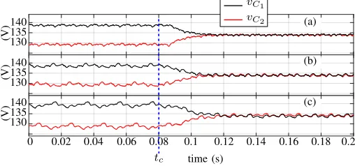
C. Balancing the Capacitor Voltages
[image:7.612.306.566.455.601.2]0 10 20 30 40 50 60 0
0.05 0.1 0.15 0.2
17th 19th22th
23th26 th
29th
[image:8.612.45.300.54.136.2]31th
Fig. 12. FFT for the phase voltage Vaf with and without even-harmonic elimination of Fig. 11.
140
130 135
140
130 135
140
130 135
0 0.02 0.04 0.06 0.08 0.1 0.12 0.14 0.16 0.18 0.2
time (s)
(a)
(b)
(c)
tc
vC1
vC2
(V)
(V)
(V)
Fig. 13. Control impact over the dc-link voltagesvC1 andvC2 under non-sinusoidal modulated voltages for (a) balanced three-phase load R=30Ω,
L=22mH and a three-phase rectifier with loadRrec=60(in parallel)(b)
RL load of phasechas been disconnected, (c)RL load of phaseband c
has been disconnected.
[image:8.612.46.300.183.302.2]the voltage references depicted by (23)-(25). Fig. 13 shows the convergence of the voltages vC1 andvC2 after implementing closed-loop control over the dc-link voltages. From Fig. 13, it can be noticed that even for a complex trajectory of the reference vector, or for different unbalanced loads, the balance of the voltages on the dc-link capacitors is simple to achieve as fas as the currents do not havedccomponents. Fig. 14 shows the neutral currents for the corresponding cases presented in Fig. 13. As expected, the converter is capable of handling the zero sequence current components through the fourth leg.
IV. CONCLUSIONS
This paper has presented a simplified SVM algorithm for a four-leg NPC converter. The proposed algorithm reduces the problem of implementing a three-dimensional modulation
0 5 10
-5 -10
0 0.02 0.04 0.06 0.08 0.1 0.12 0.14 0.16 0.18 0.2
time (s) 0
5 10
-5 -10
0 5 10
-5 -10
(a)
(b)
(c)
if
(A)
if
(A)
if
(A)
Fig. 14. Neutral currentif under non-sinusoidal modulated voltages for (a) balanced three-phase load R=30Ω, L=22mH and a three-phase rectifier with loadRrec=60(connected in parallel) (b)RLload of phasechas been disconnected, (c)RLload of phasebandchas been disconnected.
method into a much simpler two-dimensional SVM algorithm in the αβ plane. The modulation method discussed in this paper was experimentally validated in a 6kW prototype con-sidering several experimental tests. For instance the modula-tion of different voltage references and eliminamodula-tion of even-order harmonics from the output voltage signals. For all the experimental tests realised in this work, excellent results were achieved. In addition, the proposed SVM could be applied to others four-leg topologies.
The computational burden of the algorithm is also low. The execution time of the proposed SVM algorithm is less than
20µs when implemented in a control platform based on a Pentium processor.
The development of this algorithm allows implementation of overmodulation strategies for four-leg converters. Which can be explore in future publications. [27]
APPENDIX
REFERENCES
[1] F. Blaabjerg, Z. Chen, and S. B. Kjaer, “Power electronics as efficient interface in dispersed power generation systems,” Power Electronics, IEEE Transactions on, vol. 19, no. 5, pp. 1184–1194, sep 2004. [2] M. Liserre, R. Cardenas, M. Molinas, and J. Rodriguez, “Overview
of Multi-MW Wind Turbines and Wind Parks,”IEEE Transactions on Industrial Electronics, vol. 58, no. 4, pp. 1081–1095, apr 2011. [3] C. Xia, X. Gu, T. Shi, and Y. Yan, “Neutral-point potential balancing
of three-level inverters in direct-driven wind energy conversion system,” IEEE Transactions on Energy Conversion, vol. 26, no. 1, pp. 18–29, 2011.
[4] J. Nurmi, “Efficiency with usability,” ABB Report, Helsinki, Finland, 2010.
[5] M. C. Cavalcanti, A. M. Farias, K. C. Oliveira, F. A. S. Neves, and J. L. Afonso, “Eliminating Leakage Currents in Neutral Point Clamped Inverters for Photovoltaic Systems,” IEEE Transactions on Industrial Electronics, vol. 59, no. 1, pp. 435–443, jan 2012.
[6] H. R. Teymour, D. Sutanto, K. M. Muttaqi, and P. Ciufo, “Solar PV and battery storage integration using a new configuration of a three-level NPC inverter with advanced control strategy,”IEEE Transactions on Energy Conversion, vol. 29, no. 2, pp. 354–365, 2014.
[7] R. Zhang, V. Prasad, D. Boroyevich, and F. Lee, “Three-dimensional space vector modulation for four-leg voltage-source converters,” IEEE Transactions on Power Electronics, vol. 17, no. 3, pp. 314–326, may 2002.
[8] R. Cardenas, C. Juri, R. Pena, P. Wheeler, and J. Clare, “The Application of Resonant Controllers to Four-Leg Matrix Converters Feeding Unbalanced or Nonlinear Loads,”IEEE Transactions on Power Electronics, vol. 27, no. 3, pp. 1120–1129, mar 2012.
[9] R. Zhang, V. H. Prasad, D. Boroyevich, and F. C. Lee, “Three-dimensional space vector modulation for four-leg voltage-source con-verters,”IEEE Transactions on Power Electronics, vol. 17, no. 3, pp. 314–326, May 2002.
[10] Z. Liu, J. Liu, and J. Li, “Modeling, Analysis, and Mitigation of Load Neutral Point Voltage for Three-Phase Four-Leg Inverter,” IEEE Transactions on Industrial Electronics, vol. 60, no. 5, pp. 2010–2021, may 2013.
[11] R. Cardenas, R. Pena, P. Wheeler, and J. Clare, “Experimental Validation of a Space-Vector-Modulation Algorithm for Four-Leg Matrix Converters,” IEEE Transactions on Industrial Electronics, vol. 58, no. 4, pp. 1282–1293, apr 2011.
[12] P. W. Wheeler, P. Zanchetta, J. C. Clare, L. Empringham, M. Bland, and D. Katsis, “A Utility Power Supply Based on a Four-Output Leg Matrix Converter,” IEEE Transactions on Industry Applications, vol. 44, no. 1, pp. 174–186, 2008.
[image:8.612.47.301.581.703.2]TABLE IV
THE81DIFFERENT SWITCHING COMBINATIONS FOR A FOUR-LEGNPC
CONVERTER IN THEαβγSPACE.(P=1, O=0ANDN=-1)
abcVector αβγ Vector
vi abcf v i abc v i αβγ [OOOO] v0z
abc=[0,0,0] vαβγ0z =[0,0,0] [PPPP] vabc0p=[0,0,0] vαβγ0p =[0,0,0] [NNNN] v0n
abc=[0,0,0] vαβγ0n =[0,0,0] [ONNN] v1n
abc=[1,0,0] vαβγ1n =[ 2 3,0,
1 3] [POOO] vabc1p=[1,0,0] vαβγ1p =[23,0, 13] [NONN] v2n
abc=[0,1,0] v2αβγn =[-1 3, √ 3 3 , 1 3] [OPOO] vabc2p=[0,1,0] v2αβγp =[-13,
√ 3 3 ,
1 3] [NNON] vabc3n=[0,0,1] v3αβγn =[-13,
-√ 3 3 ,
1 3] [OOPO] vabc3p=[0,0,1] v3αβγp =[-1
3, -√
3 3 ,
1 3] [OONO] v4n
abc=[0,0,-1] v4αβγn =[ 1 3,
√ 3 3 ,
-1 3] [PPOP] vabc4p=[0,0,-1] v4αβγp =[13,
√ 3 3 ,
-1 3] [ONOO] v5n
abc=[0,-1,0] v5αβγn =[ 1 3,
-√ 3 3 ,
-1 3] [POPP] vabc5p=[0,-1,0] v5αβγp =[1
3, -√
3 3 ,
-1 3] [NOOO] v6n
abc=[-1,0,0] v 6n αβγ
=[-2 3,0,
-1 3] [OPPP] vabc6p=[-1,0,0] vαβγ6p =[-23,0, -13] [OONN] v7n
abc=[1,1,0] v7αβγn =[ 1 3, √ 3 3 , 2 3] [PPOO] vabc7p=[1,1,0] v7αβγp =[13,
√ 3 3 ,
2 3] [ONON] vabc8n=[1,0,1] v8αβγn =[13,
-√ 3 3 ,
2 3] [POPO] vabc8p=[1,0,1] v8αβγp =[13,
-√ 3 3 ,
2 3] [NOON] v9n
abc=[0,1,1] vαβγ9n =[-2 3,0,
2 3] [OPPO] vabc9p=[0,1,1] vαβγ9p =[-23,0, 23] [ONNO] v10n
abc=[0,-1,-1] vαβγ10n=[ 2 3,0,
-2 3] [POOP] v10abcp=[0,-1,-1] vαβγ10p=[23,0, -23] [NONO] v11n
abc=[-1,0,-1] v11αβγn =[-1 3,
√ 3 3 ,
-2 3] [OPOP] v11abcp=[-1,0,-1] v11αβγp=[-13,
√ 3 3 ,
-2 3] [NNOO] v12n
abc=[-1,-1,0] v12αβγn =[-1 3,
-√ 3 3 ,
-2 3] [OOPP] v12abcp=[-1,-1,0] v12αβγp=[-1
3, -√
3 3 ,
-2 3] [OOON] v13n
abc=[1,1,1] vαβγ13n=[0,0,1] [PPPO] v13abcp=[1,1,1] vαβγ13p=[0,0,1] [NNNO] v14n
abc=[-1,-1,-1] vαβγ14n=[0,0, -1] [OOOP] v14abcp=[-1,-1,-1] vαβγ14p=[0,0, -1]
[14] F. Rojas-Lobos, R. Kennel, and R. Cardenas-Dobson, “Current control and capacitor balancing for 4-leg NPC converters using finite set model predictive control,” inIECON 2013 - 39th Annual Conference of the IEEE Industrial Electronics Society. IEEE, nov 2013, pp. 590–595. [15] U. Jensen, F. Blaabjerg, and J. Pedersen, “A new control method
for 400-Hz ground power units for airplanes,”IEEE Transactions on Industry Applications, vol. 36, no. 1, pp. 180–187, 2000.
[16] S. Ceballos, J. Pou, J. Zaragoza, J. Martin, E. Robles, I. Gabiola, and P. Ibanez, “Efficient Modulation Technique for a Four-Leg Fault-Tolerant Neutral-Point-Clamped Inverter,”IEEE Transactions on Industrial Electronics, vol. 55, no. 3, pp. 1067–1074, mar 2008. [17] M. Rivera, V. Yaramasu, J. Rodriguez, and B. Wu, “Model
Predictive Current Control of Two-Level Four-Leg InvertersPart II: Experimental Implementation and Validation,” IEEE Transactions on Power Electronics, vol. 28, no. 7, pp. 3469–3478, jul 2013.
[18] H. Ghoreishy, Z. Zhang, O. C. Thomsen, and M. A. E. Andersen, “A fast-processing modulation strategy for three-phase four-leg neutral-point-clamped inverter based on the circuit-level decoupling concept,” inProceedings of The 7th International Power Electronics and Motion Control Conference, vol. 1. IEEE, jun 2012, pp. 274–280.
[19] U. M. Choi, H. H. Lee, and K. B. Lee, “Simple neutral-point voltage control for three-level inverters using a discontinuous pulse width modulation,”IEEE Transactions on Energy Conversion, vol. 28, no. 2,
TABLE V CONTINUATION OFTABLEV.
abcVector αβγ Vector
vi
abcf vabci vαβγi
vaz,vbz,vcz,vf z
[vi
af,vibf,vicf] [viα,viβ,viγ]
[PONO] v15
abc=[1,0,-1] v15αβγ=[1,
√ 3 3 ,0]
[OPNO] v16
abc=[0,1,-1] v16αβγ=[0, 2√3
3 ,0] [PNOO] v17abc=[1,-1,0] v17αβγ=[1,
-√ 3 3 ,0]
[ONPO] v18
abc=[0,-1,1] v 18 αβγ=[0,
-2√3 3 ,0]
[NPOO] v19
abc=[-1,1,0] v19αβγ=[-1,
√ 3 3 ,0]
[NOPO] v20
abc=[-1,0,1] v20αβγ=[1,
-√ 3 3 ,0]
[PPNO] v21
abc=[1,1,-1] v21αβγ=[ 2 3,
2√3 3 ,
1 3]
[PNPO] v22
abc=[1,-1,1] v22αβγ=[ 2 3,
-2√3 3 ,
1 3]
[NPPO] v23
abc=[-1,1,1] v23αβγ =[-4 3,0,
1 3]
[PNNO] v24
abc=[1,-1,-1] v 24 αβγ=[
4 3,0,
-1 3]
[NPNO] v25
abc=[-1,1,-1] v25αβγ =[-2 3,
2√3 3 ,
-1 3]
[NNPO] v26
abc=[-1,-1,1] v26αβγ =[-2 3,
-2√3 3 ,
-1 3]
[POON] v27
abc=[2,1,1] v 27 αβγ=[
2 3,0,
4 3]
[OPON] v28
abc=[1,2,1] v28αβγ =[-1 3, √ 3 3 , 4 3]
[OOPN] v29
abc=[1,1,2] v29αβγ =[-1 3,
-√ 3 3 ,
4 3]
[PNNN] v30
abc=[2,0,0] v30αβγ=[ 4 3,0,
2 3]
[NPNN] v31
abc=[0,2,0] v31αβγ =[-2 3,
2√3 3 ,
2 3] [NNPN] v32abc=[0,0,2] v32αβγ=[-23, -2
√ 3 3 ,
2 3]
[PPNP] v33
abc=[0,0,-2] v 33 αβγ=[
2 3,
2√3 3 ,
-2 3]
[PNPP] v34
abc=[0,-2,0] v34αβγ=[ 2 3,
-2√3 3 ,
-2 3]
[NPPP] v35
abc=[-2,0,0] v35αβγ =[-4 3,0,
-2 3]
[OONP] v36
abc=[-1,-1,-2] v36αβγ=[ 1 3,
√ 3 3 ,
-4 3]
[ONOP] v37
abc=[-1,-2,-1] v37αβγ=[ 1 3,
-√ 3 3 ,
-4 3]
[NOOP] v38
abc=[-2,-1,-1] v38αβγ =[-2 3,0,
-4 3]
[PONN] v39
abc=[2,1,0] v39αβγ=[1,
√ 3 3 ,1]
[OPNN] v40
abc=[1,2,0] v40αβγ=[0, 2√3
3 ,1] [PNON] v41abc=[2,0,1] v41αβγ=[1,
-√ 3 3 ,1]
[ONPN] v42
abc=[1,0,2] v42αβγ=[0, -2√3
3 ,1]
[NPON] v43
abc=[0,2,1] v43αβγ=[-1,
√ 3 3 ,1]
[NOPN] v44
abc=[0,1,2] v44αβγ=[1,
-√ 3 3 ,1]
[PONP] v45
abc=[0,-1,-2] v 45 αβγ=[1,
√ 3 3 , -1]
[OPNP] v46
abc=[-1,0,-2] v46αβγ=[0, 2√3
3 , -1]
[PNOP] v47
abc=[0,-2,-1] v47αβγ=[1,
-√ 3 3 , -1] [ONPP] v48abc=[-1,-2,0] v48αβγ=[0, -2
√ 3 3 , -1]
[NPOP] v49
abc=[-2,0,-1] v 49 αβγ=[-1,
√ 3 3 , -1]
[NOPP] v50
abc=[-2,-1,0] v50αβγ=[1,
-√ 3 3 , -1]
pp. 434–443, 2013.
[20] N.-c. I. Systems, U.-m. Choi, S. Member, J.-s. Lee, and S. Member, “New Modulation Strategy to Balance the Neutral-Point Voltage for Three-Level,” IEEE Trans. on Energy Conversion, vol. 29, no. 1, pp. 91–100, 2014.
[21] L. G. Franquelo, M. Prats, R. C. Portillo, J. I. L. Galvan, M. A. Perales, J. M. Carrasco, E. G. Diez, and J. L. M. Jimenez, “Three-dimensional space-vector modulation algorithm for four-leg multilevel converters using abc coordinates,” Industrial Electronics, IEEE Transactions on, vol. 53, no. 2, pp. 458–466, apr 2006.
[22] Jang-Hwan Kim and Seung-Ki Sul, “Overmodulation strategy for a three-phase four-leg voltage source converter,” in 38th IAS Annual Meeting on Conference Record of the Industry Applications Conference, 2003., vol. 1. IEEE, 2003, pp. 656–663.
of PWM inverters in the overmodulation range including the six-step mode,” in Proceedings of the 1992 International Conference on Industrial Electronics, Control, Instrumentation, and Automation. IEEE, 1992, pp. 307–312.
[24] D. Feng and D. Xu, “Space vector modulation for neutral point clamped multilevel inverter with even order harmonic elimination,” in Canadian Conference on Electrical and Computer Engineering 2004 (IEEE Cat. No.04CH37513), vol. 3. IEEE, 2004, pp. 1471–1475. [25] “519-1992 - IEEE Recommended Practices and Requirements for
Har-monic Control in Electrical Power Systems.”
[26] B. Wu,High-Power Converters and AC Drives. Wiley, 2005. [27] N. Celanovic and D. Boroyevich, “A comprehensive study of
neutral-point voltage balancing problem in three-level neutral-neutral-point-clamped voltage source pwm inverters,”IEEE Transactions on Power Electronics, vol. 15, no. 2, pp. 242–249, Mar 2000.
F´elix Rojas was born in Santiago, Chile. He re-ceived the B.Eng. and M.Sc. degrees in electrical engineering with honours in 2009, from the Univer-sidad de Santiago de Chile. In 2015, he obtained his doctoral degree from the Technical University of Munich, Germany. During his career, he has worked in research projects related to Active filter for rail-way Applications, Matrix Converters and Multilevel converters for distribution systems. Currently he is full time lecturer at the University of Santiago, Chile. His research interest are Multilevel converters for power network conditioning.
Ralph Kennel(M’90-SM’96) received the diploma degree in 1979 and the Dr.-Ing. (Ph.D.) degree in 1984 from the University of Kaiserslautern, Kaiser-slautern, Germany. From 1983 to 1999, he worked on several positions with Robert BOSCH GmbH, Stuttgart, Germany. Until 1997, he was responsible for the development of servo drives. From 1994 to 1999, he was appointed as a Visiting Professor at the University of Newcastleupon-Tyne, England, U.K. From 1999 to 2008, he was a Professor for elec-trical machines and drives at Wuppertal University, Wuppertal, Germany. Since 2008, he has been a Professor for electrical drive systems and power electronics at Technische Universtat Muenchen, Germany. His main interests today are: sensorless control of ac drives, predictive control of power electronics, and hardware-in-the-Loop systems.
Jon C. Clare(M’90-SM’04) was born in Bristol, U.K., in 1957. He received the B.Sc. and Ph.D. degrees in electrical engineering from the University of Bristol, Bristol. From 1984 to 1990, he was a Research Assistant and Lecturer with the University of Bristol, where he was involved in teaching and research on power electronic systems. Since 1990, he has been with the Power Electronics, Machines and Control Group, The University of Nottingham, Nottingham, U.K., where he is currently a Professor of power electronics. His research interests include power-electronic converters and modulation strategies, variable-speed-drive systems, and electromagnetic compatibility.

![Fig. 5. General diagram for a three-dimensional SVM. d⊺ denotes the transpose of the vector d= [d2, d3, d4]](https://thumb-us.123doks.com/thumbv2/123dok_us/8657533.374645/5.612.63.557.55.287/fig-general-diagram-dimensional-svm-denotes-transpose-vector.webp)