-
-68000 centra
processing unit
hardware reference
manual
LIMITED WARRANTY
CODATA SYSTEMS, CORP. electrical and mechanical products are warranted for a period of one hundred el.gh.ty days from the date of shipment from CODATA SYSTEMS, CORP. EquiPment supplied by CODATA SYSTEMS, CORP.
is designed and intended for use in commercial applications. This Limited Warranty provides for the repair or replacement of any product which may prove defective in materials or workmanship during this time. CODATA SYSTEMS, CORP. reserves the right to decide if the equipment will be repaired or replaced. All equipment to be repaired or replaced under terms of this Limited Warranty must be returned to a CODATA SYSTEMS CORP. Service Facility. Please see the instructions in the user's manual to arrange service under this Limited Warranty.
This Limited Warranty is not valid if the equipment has been subjected to abuse or misuse. In case of damaie to the product due to shippin&:, handling or incorrect installation, standard repair charges will be assessed.
THERE ARE NO WARRANTIES WHICH EXTEND BEYOND THE DESCRIPTION ON THE FACE HEREOF. BUYER AFFIRMS THAT HE HAS NOT RELIED ON SELLER'S SKILL OR JUDGMENT TO SELECT OR FURNISH SOFTWARE FOR ANY PARTICULAR PURPOSE AND THIS SALE IS MADE WITHOUT ANY WARRANTY BY SELLER THAT SUCH SOFTWARE IS SUIT ABLE FOR ANY PARTICULAR PURPOSE. SELLER MAKES NO WARRANTY OF MERCHANT ABILITY IN RESPECT TO THE SOFTWARE SOLD UNDER THIS AGREEMENT.
All statements repnling this Limited Warranty are contained in this document. Representatives or Distributors of CODATA SYSTEMS, CORP. products may not make any statements reguding the expansion or extension of this Limited Warranty, unless those statements are in writing and signed by a corporate officer of CODATA SYSTEMS. CORP.
05-0004-01
ILLUSTRATIONS PAGE
Figure 21 68000 Central Processing Unit
-92-1012-xx . . . . 4
Figure 2-2 - 68000 Central Processing Unit layout 6
Table 2-1 - Test Points 7
Figure 3-1 - 68000 Central Processing Unit Block
Diagram 8
Table 3-1 - 68000 CPU Logical Address Locations 11 Figure 3-2 - Memory Map Block Diagram 12 Table 3-2 - Segment Level Protection Attributes 14 Table 3-3 - Memory Map Register Bit Map 16 Figure 3-3 - On-Card 256k Byte RAM Block
Diagram 17
Figure 3·4 - Interrupt Block Diagram 19 Figure 3-5 - UART Block Diagram 20 Figure 3-6 - Timer Block Diagram 21 Figure 3-7 - 796 Bus I nterface Block Diagram 22 Figure 3-8 - Parallel Input Block Diagram 23 Figure 3-9 - Device Decoder Block Diagram 24 Figure 3-10- Power-On-Reset Block Diagram 25 Figure 3-11 - System Timing Block Diagram 26
Table 3-4 - 68000 Central Processing Unit Active
796 Bus Signals . . . . 27
Figure 3-12 - On-Card RAM Read Cycle Timing 28 Figure 3-13 - On-Card RAM Write Cycle Timing 29 Figure 3-14 - On-Card ROM Read Cycle Timing 30 Figure 3-15 - Off-Card RAM and Input Output
Read Cycle Timing . . . . . . . . 31 Figure 3-16 - Off-Card RAM and Input Output
Write Cycle Timing . . 32
Table 4-1 - 68000 Central Processing Unit
92-1 012-xx - Specifications 33
Table 5-1 - 68000 Central Processing Unit Options
PIN 91-1012-xx . . . 36
Figure 5-1 - UART Register Values 39 Figure 5-2 - Write Register 0 Routine and
Register Map . . . . 40
Figure 5-3 - Write Register 1 Routine and
Register Map . . . 40
Figure 5-4 - Write Register 2 Routine and
Register Map . . . 41 Figure 5-5 - Write Register 3 Routine and
Register Map . . . 41 Figure 5-6 - Write Register 4 Routine and
Register Map . . . . . . 42
Figure 5-7 - Write Register 5 Routine and
Register Map . . . 43 Figure 5-8 - Read UART A or B Status Routine
and Register Map . . . . . 44 Figure 5-9 - Send Data to UART A or B Routine
and Register Map . . . . . . . . . 44
Figure 5-10 - Receive Data from UART A or B
Routine 44
Page 2
I LLUSTRA TlONS
Figure 5-11 - Timer Initialization Routine Figure 5-12 - Watchdog Timer Set Up Routine Figure 5-13 - RTC and Refresh Timer Set Up Routines . . . . Figure 5-14 - RTC and Refresh Timer Clear Routine
Figure 5-15 - Values for Period Between Interrupts on Resets .
Figure 5-16 - Values for Divisor Constant Figure 5-17 - UART Timer Set Up Routines Figure 5-18 - Values of Constants Used to Program Timer Device .
Figure 7-1 - 68000 Central Processing Unit Logic Diagram
Table 7-1 - 68000 Central Processing Unit Replaceable Parts list .
Table 7-2 - Pin Assignments on 796 Bus Board Connector (Pl)
Table 7-3 - Pin Assignments on 796 Bus Board Connector (P2)
Table 7-4 - 68000 CPU Connector Pl Pin Assignments
Table 7-5 - 68000 CPU Connector P2 Pin Assignments
Table 7-6 - Pin Assignments of RS-423 Serial 10
Board Connector (Jl) .
Table 7·7 - Pin Assignments of 16-Bit Parallel Input Port (J2) . . . .
1. GENERAL
1.01 This manual provides a physical description,
functional description and operating theory for effective maintenance of the Codata Systems Corp. 68000 Central Processing Unit, 92-1012-xx.
1.02 The 68000 Central Processing Unit (CPU)
is supplied as a single printed circuit assembly (PCA) for use as a system component in the Codata Systems Corp:
(1) CT8-Series Mainframe,
(2) CTW-Series Mainframe.
Features
1.03 The 68000 CPU is a powerful single card
processor designed around the MCL68000L microprocessor (J1P) device. CPU features include:
• The 68000 pP operates at 8 MHz.
• IEEE 796 Microcomputer Bus compatible.
• Multirnaster capability.
• The entire CPU is on a single PCA.
• 20-bit 796 Bus providing 1M byte
addressing.
• A segmented, paged, memory management method.
• Up to 256k bytes of on-card parity-checked dynamic Random Access Memory (RAM). The RAM operates without wait states.
• Up to 32k bytes of on-card Read Only Memory (ROM).
• Two universal asynchronous receiver trans-mitters (UARTs) for serial input output (I/O). EIA RS-423A compatible.
• Five 16-bit timer channels.
• One 16-bit parallel input port.
• Seven level interrupt with priority set by option jumpers.
• Single +5 Vdc power requirement.
05-0004-01
NOTE
The folio wing reference notations apply in this technical manual:
(J) A
*
suffix to a single name indicates logical NOT and active low.(2) In and out references are ill respect to CPU or bus master.
(3) Ik byte equals 1,024 bytes, i.e., 64k
bytes equals 65,536 bytes.
(4) Codata Systems part numbers are
made up of eight digits, e.g., the part number of this manual is 05-0004-01.
(5) A SUffix -xx to a part number indicates the part or assembly may have more than one configuration in production, i.e., the 68000 Central Processing Unit ;s
92-1012-xx.
J400
, T I'I
, I •
.
,..
.
J900
J901
J902
P1
J903
P2
Figure 2
-
1
-
68000 Central Processing U
n
it
-
92-1012
-
xx
J101
o
<{1
o
o o
~
o
-2. PHYSICAL DESCRIPTION
2.01 The 68000 Central Processing Unit (CPU) 92-1012-xx is an integrated system com-ponent incorporating all the necessary comcom-ponent parts to provide the Mainframe with a single PCA CPU. Figure 2-1 illustrates the 68000 CPU. The PCA contains:
(1) A 68000 pP section. This is a 16-bit pP operating at 8 MHz.
(2) A Memory l'vianagement section.
(3) A Memory Control section.
(4) A 256k byte RAi\.1 section providing the
p P with up to 256k bytes of dynamic
memory independent from the Mainframe RAl\L
(5) A 32k ROM section providing the /lP with up to 32k firmware.
(6) A UART section. This provides two
RS-423A serial I/O ports for the Mainframe.
(7) A Timer sectioli providing the programmer
with five I6-bit programmable timers.
(8) A 796 Bus Interface section.
(9) A I6-bit Parallel Input Port section.
(10) A Clocks and Logic section.
Figure 2-2 illustrates the physical locations of these sections on the PCA.
2.02 The PCA measures 6.0 inches by 12.0 inches. A pair of edge-type pc con-nectors, PI and P2, mate with the 796 Bus Backplane connectors.
(1) PI is a dual 43-position, 86-conductor pc connector. The pin assignments conform to the 796 Bus specification.
IMPORTANT
The 68000 should not be installed in a backplane having the connector mating with
P2 wired to the 796 Bus specification.
05-0004-01
(2) P2 is a dual 30-position, 60-conductor pc connector. These pins are used for off-card RAM expansion. The pin assignments do not conform to the 796 Bus specification.
2.03 A pair of flat ribbon cablp reccpticals are provided at the top of the PCA for connection to external 1/0 devices.
(1) The JI connector provides data and
status/control lines from two RS-423A
data communication lines (DeL). The
50-conductor interconnect cable is terminated by two DB-25S connectors on the Mainframe Rear Panel. Refer to Table 7-6 for individual PCA pin assignments.
(2) The J2 connector provides data input lines for the I6-bit Input Port and lines for an external reset switch. Refer to Table 7-7 for individual PCA pin assignments.
2.04 Distinctive white silkscreen marking has been provided on the component side of the PCA. Component reference designators are marked where practical. They facilitate locating individual parts on the logic diagram or replaceable parts list.
Options
2.05 Several alternate features can be configured through option jumpers on the PCA. Refer to Figure 2-1.
(1) J100 configures UART B as a DeE or DTE port and selects the ROM size.
(2) J900 generates the 796 Bus control signals with or without using the 8218 device.
(3) J90I selects the source or destination of INIT* and Bus Clocks.
(4) J902 selects the interrupt levels.
Test Points
2.06 Test points for the 68000 CPU have been provided on the PCA for repair and maintenance. Table 2-1 tabulates these by location and function.
I
---
Oual
-
UART
:1
- - - • • - - - • • - • - - - -I
,I
Timer
·
Figure 2-2 - 68000 Central Processing Unit Layout
~
o
o
~
o
Reference
JI0l.! JI01.2
J400.1 J400.2 J400.3 J400.4 J400.5 J400.6 J400.7 J400.8
J903.1 J903.2 J903.3 J903.4
3. FUNCTIONAL DESCRIPTION
Overview
Table 2-1 - Test Points
Mnemonic
Halt I nd icator
vce
M.REF*NOTE
An L ED with an internal curren t limiting resistor may be installed between 1101.1 and 1101.2 to act as an indicator that the IlP is HALTED. An LED is
not supplied in the
standard peA
configuration.
General Test Points
vce
SYS.ACCESS* C62.0-31 TIMEOUT* DTACK* BERR GND GND
Memory Column Address Strobe Test Points
M.CASO* M.CASl* M.CAS2* M.CAS3*
Function
+5 Vdc
Memory Refresh - Halt
+5 Vdc
System Access 16 MHz Clock Timeout
Data Acknowledge Bus Error
Signal Ground Signal Ground
Memory CASO Memory CAS! Memory CAS2 Memory CAS3
05-0004-01
3.01 The basic function of a central processing unit (CPU) in a computing system is to
accept data and processing instructions, perform processing 0 perations and deliver the processed
data. Several additional functions are provided by the 68000 CPU besides this basic function. Figure 3-1 illustrates each function in block diagram.
05-0004-01
To External Reset Switch
J2T
Abort
~2 ~
V oltage
..
Power
Boot
S ense
..
Set
On
..
rState
..
Reset
Flip Flop
..
BOOT
1RESET HALT* READ
Clear
~r ~, ~,
Figure 3-1 - 68000 Central Processing Unit Block Diagram
05-0004-01
To RS-423
DCl
To External RAMJ1~~ ~~
P2/r"-
J2~~
""'V2 ",v2 ,..I'SO 32 ... 11'
Buffer
~~ .4~
Device Device ... )-'2 )'2 Devtce Device
Decode Decode
-"
"
Decode Decode"
32K Read 256K
5-Channel Dual Random Parallel
4
Timer ---. UART ~ Only Access
•
InputMemory
Memory Port
n .4~ .4~
..
~ .n .4~ .. ~..
~2,.. v12 ,., ,.. 1 V 8}' 1,..v 2,..1-' 13,..'" 18 ,.. 10 ,., 8,.. v 18,.. 18 '"
/ ... /
"
~,"
"
"
/ / L
/ / ./ /
"
- Interrupt
...
...
8.4~
,.y
/
-Figure 3-1 - 68000 Central Pricessing Unit Block Diagram (Cont.)
[image:10.614.70.554.106.664.2]05-0004-01
(1) 68000 microprocessor (JJP).
(2) Memory Map,
(3) Random Access Memory,
(4) Interrupt,
(5) Dual UART - Serial Input Output (I/O),
(6) Five-Channel Timer,
(7) 796 Bus Interface,
(8) Parallel Input Port,
(9) Device Decode,
(10) Power-On-Reset,
(11) System Timing.
The following paragraphs will discuss each function in detail. Figures 3-2 through 3-11 furnish detailed block diagrams of the sections. CPU timing is illustrated in Figures 3-12 through 3-16. These figures should be used in conjunction with the logic diagram, Figure 7-1, for the descriptions which follow.
68000 Microprocessor
3.02 The principle device on the CPU is the
68000 JJP. This is a high-performance JJP with 32-bit architecture and a large uniform
memory space. This JJP features sixteen 32-bit
registers divided into two sets of eight address registers and eight data registers.
3.03 The IlP instruction set and addressing
modes are both extremely regular in their implementation with a minimum of special cases thus making high-level language code generation fairly simple.
3.04 The JJ P manipulates three major data
formats:
(1) 8-bit words,
(2) 1S-bit words,
(3) 32-bit words .
... '0
The JJP can operate in supervisor or user states. assuring a secure operating system. The 68000 CPU
has been designed to fully utilize the high
performance of the JJP by providing on-card RAM that will operate without wait states at the 8 MHz speed of the system.
Bus Structure
3.05 The 68000 CPU has two principle data
busses:
(1) An internal 16-bit synchronous bus to communicate with on-card RAM/ROM and I/O devices. Since on-card accesses do not require the 796 Bus, the 796 Bus is available for use by other 796 Bus Masters, e.g., Diskette or Winchester Disk Controllers.
(2) The 796 Bus for accessing off-card RAM
and I/O devices.
NOTE
While the CPU has complete access to the 796 Bus, the 796 Bus cannot access on-cord
memory or I/O devices.
Accesses to 796 Bus devices are slower than on-card devices. The JlP cycles are stretched by an amount appropriate to the 796 Bus device being accessed. Refer to Figures 3-15 and 3-16.
3.06 The 68000 CPU is initialized through a
reset which can be activated through several channels. The reset logic is detailed in 3.54 below.
3.07 The Jl P is reset when both the HAL T* and
RESET* lines are held low. A card reset
can be initiated by the Jl P noting the logical condition of these two lines and holding the RESET* line low.
3.08 Several operations take place after a reset:
(1) The Boot State Flip-Flop is set and the boot state is entered.
(2) The Device Decode enables the Read Only
(3) Instructions stored in ROM are overlaid into address space normally occupied by RAM starting at location 000 OOOH. These instructions form what is usually called the Boot Strap process. During this process, the exception vectors located at address 000 008H to 000 OFFH are copied to RAM by reading the data from ROM and writing the data to RAM. This process is called shadow RAM.
( 4) The last instruction in the boot strap program is a write to ROM location 200 OOOH causing the Device Decode to clear
the Boot State Flip Flop.
(5) After the Boot State Flip Flop has cleared the ROM, instructions are removed from 000 OOOH and the RAM locations become available for program variables, e.g., exception vectors and program. The boot state is exited.
Addressing
3.09 Table 3·1 lists the 68000 CPU address
mapping for memory-managed RAM, and
05-0004-01
all on-card devices. All addresses above 200 OOOH are not memory managed and are absolute addresses for the named devices.
ROM
3.10 Up to 32k bytes of ROM may be installed
on the 68000 CPU in two separate groups, ROM 0 and ROM 1, whose addresses begin at 200 OOOH and 400 OOOH, respectively. The ROM 0 group is also addressed starting at location 000 OOOH while the 68000 CPU is in boot state.
3.11 Sockets on the printed circuit assembly
provide for three ROM types:
(1) The 2716 device for two groups of 2k x 16-bit words or 8k bytes.
(2) The 2732 device for two groups of 4k x 16.bit words or 16k bytes.
(3) The 2764 device for two groups of 8k x IS-bit words or 32k bytes.
Table 3-1 - Logical Address Locations
Address
Function
From To
000 OOOH IFF FFFH Mapped RAM and 1/01
200 OOOH 3FF FFFH ROM 0
400 OOOH 5FF FFFH ROM 1
SOO OOOH 7FF FFFH UART AandB
800 OOOH 9FF FFFH Five Channel Timer
AOO OOOH BFF FFFH Page Map (read/write)
COO OOOH DFF FFFH Segment Map (read/write) Context Register (read)
EOO OOOH FFF FFFH Context Register (write) 16-bit Input Port (read)
Note:
(1) Durina Boot State. Boot Strap inAructiona stored in ROM are lhadowed into this area startinJ at 000 OOOH.
[image:12.614.167.468.394.692.2]05-0004-01
Page 12
Logical Address Internal Addess Bus A 1-A23
Internal Data Bus
012-015
'....oIL .... , 4 /
012-015
4 .... ~
~,
Context WE.CX
* ---.
RegisterOE.CX*
•
4 Bit BufferCXOto
~;CX3
Address
A15 A11 A1 to to to A20 A14 A10
18
~,
WE.SMAP*
--_e_---_::
Segment Map 12-Bit x 1024
RAM CE.SMAP* . .
...
_
...
"12-Bit Transfer
Gate
Data II~
'12
I.L 12L .. /
... , ... '~2
XA15-XA22 XA15 / to
~---/---'~~XA20
I 4 '0
2-11 XA21-XA22
~,
Unused
Address
WE.PMAP* - - - -... ~
CE.PMAP* --,
Page Map
16-Bit x1024
RAM
[image:13.616.111.514.66.681.2]...
."...
_
...
, .... 00-016 ...
... ,
,
...
16-Bit Data Transfer .... 4 ~
N ... ~---~~~,.---~~/
Gate
/
/
Page Address Unused MA 11-MA 19 A 1-A 10 Control Space \ /
2o-Bit Physical
AddressMemory Management - General
3.12 The 68000 CPU employs a segmented,
paged memory management method to facilitate the effective use of memory in large
and complex programs. The ~P is aware of an
address space which is 24 bits wide. Thus the ~p
can directly address 16M bytes of memory. Multi-user 16M byte systems, however, require addressing methods which are more sophisticated than just a linear array of bytes ranging from
o
to 16M bytes. There is a need to partition user programs into separate logical address spaces such as execute-only code, read-only data, stack area and so on. This need is met by dividing programs into segments. There is a need for efficient management of the physical layout and allocation of such large address spaces and support features such as demand paging in a virtual memory system. This need is met by dividing the address spaces into pages.3.13 A multi-tasking operating system needs
a means to switch quickly between
contexts, that is, to have the CPU work on a new program while a previous program is suspended, e.g., waiting for some peripheral transfer to complete. This need is met by providing separate contexts, addressed through a context register, which points the CPU at a fresh set of segments and pages. Figure 3-2 illustrates the Memory
Management in block diagram.
3. 14 The Memory Management section provides
address translation, sharing and memory allocation control for multiple processes executing on the CPU. The address space is divided into pages of 2k bytes each. The page address bits, AO through A10, pass through the translation process unmodified. Address bits, All through A20, are subject to translation. Bits A21 through A23 are reserved for special system functions and take no part in the address translation. The maximum logical address space for a process on the CPU is thus 21 bits or 2M bytes. This 21-bit address is further extended with a four-bit Context Register also known as the process or user number.
3.15 The 23-bit logical addresses, A1 through
A23, from the J.l.P are translated into 20-bit physical addresses in two stages. In the first stage, the logical address from the ~P is translated by the Segment Map look-up table into a virtual
address, XAl5-XA20. In the second stage, this
05-0004-01
virtual address is translated by the Page Map
look-up table into a 20-bit physical address, A1-A10 and MA11-MA19.
3.16 AO is not generated by the J.l. P. The Jl P uses LDS* and UDS* to select the appropriate byte or bytes from a lS-bit word addressed by AI-A23. AO is generated by other hardware on the 68000 CPU only for use in 796 Bus accesses.
3.17 Protection is associated with the Segment
Map. Four protection bits, PROTO-PROT3,
are provided or disallow read, write and execute access to two levels, the system level and the user level. Refer to Table 3-2.
3.18 Page access control and address space
control are provided at the page map level. Page access control consists of two bits which remember that a page has been referenced, used and written to, dirty. Address space control deter-mines in which physical address space, on-card or off-card 796 Bus, a page is located as well as whether it references memory or input/output. Since no input/output addressing is done on card by the Memory Management System, this designa-tion is interpreted as an invalid page in which case a reference to a word in that page causes a page default.
Memory Management - Context Register
3.19 In a system with multiple executing
processes, it is important to be able to switch quickly between processes without having to reload all the state information relating to the address translation for a particular process. The
Context Register is a four-bit register, writable
and readable under supervisor controls, that selects one of 16 unique sections of the Segment Map. This memory management method can thus con-tain the maps for 16 distinct process or user translations at the same time.
Memory Management - Segment Map
3.20 The Segment Map is a 1024 entry table
indexed by the four-bit Context Register and the six most significant bits of the logical address, A15-A20. The output of the Segment
Map is six virtual address bits, XA15-XA20, and four protection bits, PROTO-PROT3. Each context thus has up to 64 segments and each segment has
05-0004-01
Table 3-2 - Segment Level Protection Attributes
Protect
Code PR3 PR2
0 0 0
1 0 0
2 0 0
3 0 0
4 0 1
5 0 1
6 0 1
7 0 1
8 1 0
9 1 0
10 1 0
11 1 0
12 1 1 13 1 1
14 1 1
15 1 1
Note.:
(1) r " read.
(2) w - write.
(3) x - execute
(4) -= attribute not enabled.
individual protection attributes. Segments may be
kept private to a process or shared with other processes. The six-bit virtual address from a segment entry refers to a block of 16 consecutive page entries in the Page Map. A segment can be as large as 32k bytes by using all 16 of the associated Page Map entries. A segment may be as small as 2k bytes by invalidating the unused page entries
in the Page Map. By concatenating consecutive
Segment Map entries, a process can have a single address space of 2M bytes.
Memory Management - Segment Level Protection
3.21 Each entry in the segment table contains four bits of protection information which may be used to control the access rights of that specific portion of the logical address space.
Page 14
Access Allowed PR1 0 0 1 1 0 0 1 1 0 0 1 1 0 0 1 1
PRO System User
0 -
-
-
-
-1
-
-
x-
-0 r
- -
--
-1 r
-
x-
-0 r w - -
-
-1 r w x-
-0 r
-
-
r-1 r w - r
-
-0 r
- -
r w -1 r w - r w-0 r w - r - x
1 r w - r w x
0 r
-
x r-
x1 r w x r
-
x0 r w x - - x
1 r w x r w x
The access codes are assigned to the Unix® notation TWX where:
(1) r is read access allowed,
(2) w is write access allowed,
(3) x refers to execute-only access allowed,
(4) - denote absence of that privilege.
Full access is denoted rwxrwx where the first rwx applies to system access and the second rwx
to user access. The assignment of the four-bit protection code to the six-level protection is
Memory Management - Page Map
3.22 In the Page Map the six-bit virtual address from the Segment Map and the next four logical address bits from the J1 P are translated into a physical address and a physical address space. Each segment virtual address refers to a block of 16 consecutive page entries in the Page Map.
3.23 The output of the Page Map is the upper nine bits of the physical address which is
concatenated with the lower 11 bits of the logical address to form a 20-bit Physical Address.
3.24 As well as determining the upper nine bits of the physical address, a page entry also determines to which physical address space the address belongs. By setting the address space control bits appropriately, a page may be declared to be in one of these address spaces:
(1) 0 - On-card memory space,
(2) 1 - Invalid page,
(3) 2 -796 Bus RAM,
(4) 3 - 796 Bus I/O.
Notice that each of these address spaces is 20 bits or 1M bytes even though the on-card memory is at most 256k bytes and the off-card memory is at most 1M byte. It is up to the supervisory software to initialize the memory management segment and page maps correctly for a particular system configuration.
Memory Management - Page Control
3.25 Each Page Map entry has two bits of page access control information. The referenced bit, often called the used bit, indicates that this page has been referenced:
(1) Data read reference,
(2) Data write reference,
(3) Execute reference.
The modified bit, often called the dirty bit, indicates that this page has been written to. These bits are automatically updated on every valid mapped reference. These bits are intended for future use in virtual memory systems as
described below. Refer to Table 3-3.
05-0004-01
Memory Management - Virtual Memory
3.26 The page map organization, together with the page control bits, provide enough information to implement virtual memory and demand paging.
3.27 The current implementation of the J1P cannot recover from page faults to the extent required. Specifically, it does not store enough internal state information to be able to restart an instruction which was aborted because of a page fault. However, by limiting the set of operations that can cause page faults, it is possible to provide a limited form of virtual memory capability. For example, limiting virtual memory access to load and store operations makes recovery possible. Thus virtual data spaces can be achieved. The current version of the CPU does not yet employ virtual memory.
Allocation of Logical Address Space
3.28 The 68000 CPU does not provide the
capability to access the full 16M bytes of memory that the JJ. P address lines will accommo-date. Rather, the logical address space of the pP has been allocated to various device functions. The address allocation is described in Table 3-1 and 3-3. Note the dual functions of the Segment Map and the Context Register locations. On a write to an entry, the upper four bits of the data are ignored and only the lower twelve bits are used to write to a segment entry. On a read from a
Seg-ment Map entry, the upper four bits are the
con-tents of the Context Register and the lower twelve bits are the contents of the addressed Segment
Map. On a write to location EOD OOOH, data is written to the Context Register. On a read from location EOO OOOH, data is read from the J 6-Bil
Input Port.
On-Card 256k RAM
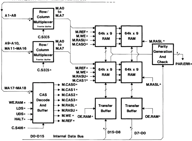
3.29 Figure 3-3 illustrates the 256k Random Access Memory in block diagram. 64k dynamic RAM devices are used to implement the on-card RAM. The RAM is organized as follows:
(1) Two 64k x IS-bit word banks, 0 and 1, on-card with provision to expand to an additional two banks off-card,
(2) Each bank is divided into an upper and lower byte.
I
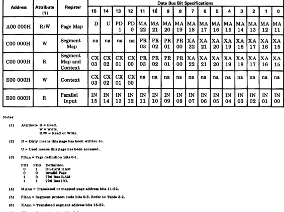
..a mTable 3-3 - Memory Management Register Bit Map
Data Bus Bit Specifications
Address Attribute Register
1d
(1 ) 15 14 13 12 11 9 8 7 6 5
AOO OOOH
R/W
Page Map
D U PDPD MA MA MA MA MA MA MA
1 0 22 21 20 19 18 17 16
eoo
OOOH
W
Segment
Map
na na na na PR PR PR PR XA XA XA
03 02 0100 22 21 20
Segment
ex ex ex ex
PR PR PR PR XA XA
XACOO OOOH
R
Map and
03 02 01 00 03 02 01 00 22 21 20Context
EOO OOOH
W
Context
CX
03 02 01cx
ex
cx
00na na na na na na na
EOO OOOH
R
Parallel
Input
15 14 13 12 11 10 09 08 07 06 05IN IN
ININ
ININ IN IN IN IN IN
Notes:
(1) Attribute R = Read.
W = Write.
R/W - Read or Write.
(2) D - Dirty meaDI this pap has been written to. U - Used means this paae has been accQI8d.
(3) PDnn'" Pale definition Biu 0-1.
PDl PDO Definition
o 1 On-Card. RAM
o 0 Invalid Pqe 1 0 796 Bus RAM 1 1 796 Bus 1/0.
(4) MAnn "" TraIulated or mapped. pqe addre. biu 11-22. (6) PRnn - SelMent protect code biu 0-3. Refer to Table 3-2.
(6) XAnn - Translated _lDlent addre .. bits 1~22.
(7) cXnn - Context relister bits 0-3.
(8) INnn - 16-bit parallel input rea.tez bits 0-15.
4 3 2 1 0
MA MA MA MA MA
15 14 13 12 11
XA XA XA XA XA
19 18 17 16 15
XA
XA
XAXA XA
19 18 17 16 15
na na
nana na
IN
IN IN IN IN
[image:17.784.109.675.60.483.2]-...
A 1-A 1 O,MA 11-MA 18 Internal Address Bus
A1-A8
A9-A10,
MA11-MA16
... - - -.. M.AO
Row/
Column
to
M.A7
8
Multiplexer
8
Trant.r Buff.r
C.S3IS
... - -... M.AO
Row/
Column
Multiplexer
Trant., Buffer
to
M.A7
M.REF*
M.WE*
M.RASU*
M.CASO*
64k x 9
RAM
64k x 9
RAM
M.RASL*
Parity
Generation
~---~~----4
And
2.... _C_h ..
e_ck_ .. PAR.ERR*
MA17-MA18
WE. RAM *
LOS*
UDS*
HALT*
C.S3Is*
CAS
Decode
And
Buffer
C.S416*
--~00-015
M.REF*
M.WE*
M.RASU*
M.CAS1*
M.CASO*
M.CAS1 *
M.CAS2*
M.CAS3*
64k x
9
RAM
M.RASL *
Transfer
M.RASU *
Buffer
M.
WE*
OE.RAM
*
....
-
...
-
..
M.REF*
D15-D8
Internal Data Bus
64k x 9
RAM
Transfer
Buffer
M.RASL*
---.---,
OE.RAM*
07-00
[image:18.782.66.740.71.567.2]05-0004-01
Bit 9 is used for byte parity checking. The organization of memory is in bytes. Read and write operations are performed in words.
NOTE
The 796 Bus pro vides both byte and word addressing. The 68000 #IP performs full word addressing, i.e., the least significant bit, A 0, is not used for internal addressing operations.
3.30 The internal data and address lines are
passed through Transfer Buffers. The data Transfer Buffers are transceivers. These Transfer
Buffers are provided for several reasons:
(1) Testing of memory is facilitated by isolating RAM from the internal address and data busses.
(2) They furnish load buffering for internal address and data busses.
3.31 Internal Address Lines, MAI7-MAI8, are
decoded and buffered to form column address strobe lines, M.CASO*-M.CAS3*. These lines are also used to select the bank.
3.32 #IP Control Signals:
(1) UDS*, upper data strobe, becomes M.UDS* and selects the upper byte of the bank,
(2) LDS*, lower data strobe, becomes M.LDS* and selects the lower byte of the bank.
3.33 Device decoder signal write enable RAM, WE.RAM*, becomes M.WE* the strobe for writing into RAM.
3.34 To read a word from RAM:
(1) UDS* and LDS* are asserted,
(2) M.CASO*·M.CAS3* selects the bank,
(3) OE.RAM* active.
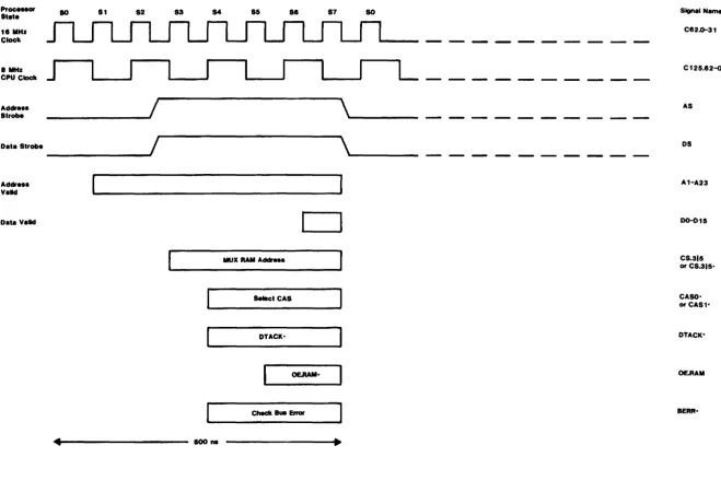
Refer to Figure 3-12 for the timing relationships.
Page 18
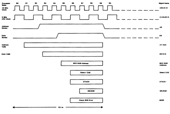
3.35 To write a word to RAM:
(1) UDS* and LDS* are asserted,
(2) M.CASO*-MCAS3* selects the bank,
(3) M.WE* is asserted.
Refer to Figure 3-13 for the timing relationships.
3.36 The row address strobe lines, M.RASU*
and M. RASL*, which are associated with
the upper and lower byte are common to
banks.
3.37 The Parity Generation and Check generates
the parity for the upper and lower byte simultaneously and stores the parity bits in bit positions designated D L and D U for lower and upper bytes respectively.
3.38 Parity checking is performed by checking
parity of bytes, DO-D7, and D8-DI5, and comparing with the respective parity bits DL and DU. A detected parity error activates P AR.ERR* which causes a bus error. Refer to 5.33.
Interrupt
3.39 The 68000 CPU has seven interrupt levels
numbered 1 through 7. Level 7 is the highest priority and level 1 is the lowest priority. At any time the 68000 CPU has an interrupt priority number set as part of the J.LP status register. Interrupts are acknowledged for all priority levels greater than the current Jl P priority contained in the JlP status register. Interrupts are prohibited for all priority levels less than or equal to the current JlP priority contained in the process status register. When an interrupt is acknowledged, the JlP priority is set to the level of the interrupt request. Figure 3-4 illustrates the interrupt in block diagram.
3.40 A level 7 interrupt is special in that it is
acknowledged even if the mask in the 68000 #IP status register is set to 7. This means that the level 7 interrupt is a non-maskable
interrupt. A level 7 interrupt is acknowledged every time the interrupt request changes from a lower level to a level 7, that is, level 7 interrupts
3.41 The 796 Bus Specification defines eight interrupt lines, INTO* through INT7* with INTO* being the highest priority. The standard also recommends that interrupts be level triggered instead of edge triggered to provide for multiple interrupt sources on each interrupt line.
3.42 Option jumpers are provided if alternate interrupt assignments are needed.
05-0004-01
IMPORTANT
To avoid confusion for MCL68000L device programmers, the number designation of the interrupt lines of the 796 Bus and the interrupt priorities were made to correspond to the definition of the MCL68000L device. INT7- on the 796 Bus is the highest priority interrupt, and INTI- is the lowest priority. INTO- is not implemented. INT7- is non-maskable and edge triggered, whereas all other interrupts are maskable and lel'el triggered.
From 796 Bus
C125.62-o
~
BOOT
/
B.INTO*
B.lNT2*
B.INT4*
B.lNT6*
B.INT1*
B.INT3*
B.INT5*
B.lNT7*
~Ir ~~ ~~ ~r
t
,.
~~ ~Ir9
15r
t
r
5 03 01 [image:20.618.62.572.155.690.2]< 1. )14 )12 10 (
.
C 4 C 2...
...
~,
...
Unused
......
...
." ." ~, ~, ~, ,IF ~,
...
eLKBuffer Register
..
"
l'l ~~ c'l~~
.. (~,
,Ir{'
,Ir('
,~0 1 2 3 4 5
•
7...
E1Priority Encoder
-P"w
() ~) I)
"
,.
~,IPLO* IPL 1 * IPL2
*
"-
/To 68000 uP
Figure 3-4 - Interrupt Block Diagram
J9
02
C.REFRESH*
C.TlMER2*
INT.SIO*
05-0004-01
3.43 Three interrupt lines INT7*, INT6* and
INTS* are option jumpered to on-card devices. The interrupt lines available for system use are:
(1) INT7* - Refresh Timer, C.REFRESH*,
highest priority, non-maskable,
(2) INT6* - User Timer, C.TIMER2*,
(3) INTS* - UART A and B, INT.SIO*,
(4) INT4* - unassigned,
(5) INT3
* -
unassigned,(6) INT2
* -
unassigned,(7) INTI * - unassigned lowest priority, and
(8) INTO* - not available.
D8-o15
A1-A2
R/W*
W/R*
C.P1
/...
,..
/ ...,
...
..,....
...
P"'"'r
-
..r
--
--...Dual
UART
DO-D7TXDA
WAo
RD'" AXDA
AXCA
TXDB TXCA
AXCB RXDB
TXCB
...
~ ......
..
...
...
...
'-3.44 The seven interrupt lines are clocked
through the Buffer Register to the Priority
Encoder and output as three encoded linest
IPLO*-IPL2*, to the IlP. BOOT is asserted during the boot state to inhibit interrupts.
3.45 'The 68000 CPU acknowledges interrupts
in an auto-vector mode. That is, the 68000 CPU generates the interrupt vector internally rather than it being supplied by the device. 'Thus the INT A * signal of the 796 Bus is never asserted and the 796 Bus vectored interrupt capabilities are not used.
Dual UART
3.46 The Dual UAR T device provides two
asynchronous serial 1/0 channels to the
RS-423A Drivers and Receivers. Refer to Figure 3-S.
Jumper option, JIOO, provides for Channel B to be configured as a DCE or DTE port.
+5Vdc
~, -5Vdc Generator ."..
A8-423
...
Driver •... AS-423 ~
Aece .. er.
...
~
J100 1_ _2
~ ~
3_ _4
-v ~
+5Vdc
J1
U
I.,
1 / I.,
1 / I I I~
II I I " J/ I I
2
3
5
13
28
C.P2
CE.SOI*
C250.125-0
(4MHz Clock)
..,..CE INT·
..
...
I NT.SI 0
*
I
II'
30
~
•
..
Figure 3-5 - UART Block Diawam
3.47 Both UART channels are almost identical, the minor differences being in the raising of interrupt pending status.
3.48 A 7201 Multi-Protocol Serial Controller device is used for the U AR T. This device can handle a number of different signal formats and is software programmable.
3.49 The data rate of Channels A and B can be
set independently under software control. Two channels from the Timer, CP.l and CP.2, furnish the clocking to the UARTs. Refer to 5.14 and 5.37 for programming of UARTs and Timer.
3.50 The EIA R~423A specification was selected
for several reasons:
(1) The R~423A is downward compatible with RS-232C,
(2) The RS-423A allows higher data rates than
R~232C,
(3) The RS-423A can support longer cable lengths than RS-232C.
Five Channel Timer
3.51 A 9513 Counter/Timer device is used to
implement the Five Channel Tim er. Refer
00-015
A1
From [OE.TIMERS*
Device
Decoder
WE.TIMERS*
C250. 125-0 (4MHz Clock)
....
/..
DO-D15.... '18 po
..
..
..
.-~
..
-..
...
Timer
05-0004-01
to Figure 3-6. Four of the five timers are pre-assigned to specific functions on the 68000 CPU. One timer is available for user-programmed timing functions. The timer channels are assigned as follows:
(1) Watchdog Timer, C.TIMER1, furnishes a programmable abort/reset capability in case the J.l. P should unexpectedly halt,
(2) RTC Timer, C.TIMER2, furnishes a user interrupt on a programmably selectable time base,
(3) Refresh Timer, C.REFRESH, furnishes an interrupt to execute dynamic RAM refresh program,
(4) UART A, C.Pl, furnishes UART Channel A clock,
(5) UART B, C.P2, furnishes UART Channel B clock.
3.52 The Five-Channel Timer clock, C250.125-0,
is a 4 MHz clock derived from a 16 MHz crystal oscillator in the System Timing section.
796 Bus Interface
3.53 Figure 3-7 illustrates the 796 Bus Interface
in block diagram.
OUT1
..
...
OUT2 --...
..
OUT3
..
..
OUT4
..
..
OUT5
...
..
C.TIMER 1 (Abort/Reset)
C. nMER2 (User Timer
Interrupt)
C.REFRESH (Refresh
Interrupt)
C.P1 (UART A Clock-x16)
C.P2 (UART B Clock-x 16)
Figure 3-6 - Timer Block Diagram
05-0004-01
UDS*
LOS*
ADEN *
Clock
~....
A 1-A 10,MA 11-MA 19
Internal Address Bus
..
LSB
...
...
...
Address
..
...
. /
..
Generator
,
...
00-015 Internal Data Bus
18/ ..
, ...
Address
20L --..
Transfer
,...
B.AO *-B.A 19*
AO
Buffer
~
...
t
...
...
B.BHEN*
Data
/
...
Transfer
...
,..
'18 ... ... '18'"
B.DO *-8.0 15
*
Buffer
~~CE.WORO*
~~To
796
Bus
ADEN *
I
B*/L
~...
OS
..
..
AS
..
...
796
Bus
MRDC*
..
...
Control
MWTC*
..
...
Logic
IOWC*
~...
IORC*
--....
CE.BYTE
..
...
...
...
..
...
...
...
...
..
.......
..
...
..
...
.......
...
....
........
*
B.lOWC*
B.MWTC*
B.lORC*
B.MRDC*
B.BUSY*
B.BREQ*
B.PRO*
B.BPRN*
B.BCLK*
B.INIT*
Figure 3-7 - 796 Bus Interface Block Diagram
Parallel Input Port
3.54 The 16-Bit Pllrallellnput Port can be used
as a general purpose 16-bit input port.
Refer to Figure 3-8.
3.55 Several auxiliary lines are extended out to
PCA connector, J2, for user applications:
(1) +5 Vdc,
... 22
(2) Signal ground,
(3) SET.INIT* pulled low, e.g., external switch closure will initiate a 68000 CPU reset,
(4) M.REF* active low indicates the IlP is
1
I I
2~
I
3
5
I I
6~
•
•
•
+5 Vdc
+5 Vdc
•
•
•
+5Vdc
16-8it
Buffer
•
•
•
29
I+5 Vdc
I30~
I
31
I
I
32~
•
•
OE.PORT*
•
SET.INIT*
M.REF*
+5Vdc
3-8 - Parallel Input Bloc
Figure
05-0004-01
Internal Data Bus
k Diagram
05-0004-01
p
.. UnusedA23 -.-.... Address h. .. CE.PROMO*
A22 -.-.... 0- ... CE.SIO*
Space
A21
...
f-\. I'-' ~ CE.PROM1*
-.-BOOTREAD
..
... Decoder r'\. h. .. CE.SPARE* -;. CE.PMAP*
FC2 ......
ROM 32x8 ~• CE.SMAP*
...,
r....
I'-'
Q
DS* ... ....
(
b-
-+
WE.SMAP * A23 _---100.w P -po CLR.BOOT*A22
~
Addressb-
..
WE.TIMER * A21 ; Spaceb
.. OE.TlMER
* R/W*
::
Decoderc-
~
WE.PMAP
*FC2
~
ROM 32x8p.---.
WE.CX*o
..
OE.CX*0- . . OE.PORT
*
....
_-_
..
SYS.ACCESS *
From
[
~TO
PROT 1..
... ....Segment Map PROT2 ...
...
Protect -;. SMAP.ERR * PROT3 ~...
Decode 4
[
FCO..
..
ROM FROM 68000 uP FC1...
512x2...
FC2
..
..
RlW*...
EN.ACCESS*
OS
JY
--r
PMAP.ERR*ok..-I'-'
• MRDC*
R*/W -;'1tD 1 h. -;.. MWTC*
J
Contr~
~
101M
* ~ A1 2~ ..., -;.. IORC* LogicB*/L . . A2Decoder 3 ::>--
.. IOWC*
OS ---...
..
4h.. ~ OE.RAM*)
ToOn
I'-'CS.S/7*
-.
..
5~ ... ,. WERAM* ao.dRAM-
e'""- .~U1used
'"P\.<
7h.... ..., ~ lhIsed
Figure 3-9 - Device Decoder Block Diagram
Device Decode
3.56 The Device Decoder is detailed in Figure 3-9.
The 68000 CPU internal address and control lines are decoded and used to enable memory management functions:
(1) Write Enable Control Register, WE.CX*,
(2) Output Enable Control Register, OE.CX*,
(3) Write Enable Segment Map, WE.SMAP*,
(4) Chip Enable Segment Map, CE.SMAP*,
(5) Write Enable Page Map, WE.PMAP*,
(6) Chip Enable Page Map, CE.PMAP*,
and to enable five-channel timer functions:
(7) Write Enable Timer, WE.TIMER*,
+SVdc
C.TlMER1
*
oc+5 Vdc
R301
R300
Threshold ...
Voltage
oc ____Detector
R302
C304
05-0004-01
(8) Output Enable Timer, OE.TIMER*,
and to enable 32k ROM:
(9) Chip Enable ROMO, CE.PROMO*,
(10) Chip Enable ROMl, CE.PROMI *,
and clear the boot state:
(11) Clear Boot, CLR.BOOT*,
and enable the 16-Bit Parallel Input Port:
(12) Output Enable Port, OE.PORT*.
Power-On- Reset
3.57 Refer to Power-On-Reset block diagram,
Figure 3-10, for the description which follows. A reset, RESET* and HALT*, can be initiated through several channels.
oc
INIT
J902
SET.INIT
*
INIT
oc
HALT*
INIT*
To
68000
uP
B.INIT*
To
796 Bus
J2
External
I
r
Reset
Figure 3-10 - Power-On-Reset Block Diagram
05-0004-01
(1) The Voltage Threshold Detector monitors the +5 Vdc supply for a change. When the voltage is greater than 4.65 V, the reset is
removed. If the voltage falls below 4.25 V, a reset is issued, e.g., when the Mainframe is
powered on or the line voltage suddenly drops,
(2) The Watchdog Timer determines that the /1 P has halted and activates C. TIMER1 *,
(3) An INIT* is issued from the 796 Bus. Jumper Option J902 provides for issuing an INIT* to the 796 Bus,
(4) An external switch closure from J2 the
Parallel Input Port Connector.
System Timing
3.58 A 16 MHz crystal-controUed oscillator is
used in the System Timing to count down to:
(1) 8 MHz - CI25.62-0 for the /1P clock,
(2) 4 MHz - C250.125-0 for the Five Channel Timer.
Refer to Figure 3-11.
3.59 C.S315 through C.SI0 112 are generated
in a 8-bit Shift Register clocked by the buffered 16 MHz line.
3.60 796 Bus TIMEOUT* is issued from the
4-Bit Counter.
+2 ....
..
C12S.62-o
4-Bit
~C250.12S-o
---.
+4 ....Counter
ADEN
:: T~P
4-Bit
..
CARRY ....
TIMEOUT
16 MHz
..
Counter
.... CLK
Oscillator
C62.0-31
CLRf
AS
..
C.S 315
+SVdc
..
..
SA..
....C.S 416
....
Buffer
8-Bit
..
....C.S 517
Y>
..
..
C.S 618
Shift
..
...
CPC.S 719
...
..
Register
...
...
C.S 8110
...
...
C.S 9111
...
C.s 10112
..
CR
U
,0
OS
05-0004-01
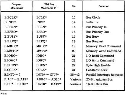
Table 3-4 - 68000 Central Processing Unit Active 796 Bus Signals
Diagram 796 Bus
Pin Function
Mnemonic Mnemonic (1)
B.BCLK* BCLK* 13 Bus Clock B.INIT* INIT* 14 Initialize B.BPRN* BPRN* 15 Bus Priority In B.BPRO* BPRO* 16 Bus Priority Out B.BUSY* BUSY* 17 Bus Busy
B.BREQ* BREQ* 18 Bus Request
B.MRDC* MRDC* 19 Memory Read Command B.MWTC* MWTC* 20 Memory Write Command B.IORC* IORC* 21 I/O Read Command B.IOWC* IOWC* 22 I/O Write Command B.BHEN* BHEN* 27 Byte High Enable B.CCLK* CCLK* 31 Constant Clock
B.INTO --7 INTO* - INT7 * 35-42 Parallel Interrupt Requests B.AO* - B.A19* ADRO* - ADI0* Various 20-Bit Address Bus
B.DO* - B.D16* DATO*-DATF* Various 16-Bit Data Bus
Note:
(1) Address and data bus lines are In hexadecimal notation.
I
Proc . . . . 10 S1 S2 S3 S4 IS S8 S7 80 Signal Neme~
Stete§
~ 1811Hz C82.o-31
~
Clock
-
-
-
----
--
-
--0
-a
811Hz
J
L
C125.fS2-oCPU Ciodl
-
--
-
-
-- - - --
--
--/
\
AckIr . . . AS
Strobe
- - -
--
--
-
--
-
--
--/
\
Date Strobe DS
-
-
-
-
- -
- -
-
-Addre . . A1-A23
Veld
Date Veld
CJ
D0-015IlUX RAIl Addren CS.3Is
or CS.3IS'
Select CAS CASO'
or CAS1'
DTACK' DTACK'
0EJlAII· OEJtAM
Check 8_ EmIr BERR'
[image:29.784.60.719.44.505.2]..
500 ne..
Proceuor
Stat.
1811Hz
Clock
8 MHz CPU Clock AckIr . . . Strobe Date Strobe
Acldr . . . Vald
Oat. Veld
J
_ _
----'f
_ _ _ _
-.-..J/
L
\ _
-IIUX RAil Acid,. . .
S.lect CAl
DTACK"
WE.RAM·
Check BUS Error 82
n.
Figure 3-13 - On-Card RAM Write Cycle Timing
SIgn.IN.,.,. C82.o-31
C12S.82-o
AS
OS
A1-A23
00-015
IIUX RAil
Addr ••• Select CAS
DTACK'
WE.RAII·
[image:30.782.61.730.62.511.2]I
Proceuor 80 81 S2 83 S5 58 S7 88 58 510 511 S12 513 SO Signal Nam. ~aut. b
~ 1811Hz C82.0-31
I
Clock
b
~
811Hz
J
L
C125.U-QCPU Clock
/
Addre ••
\
ASStroH
/
ON
\
OSStrobe
Addr ••• A1-A23
Veld
Data Vald
CJ
00-015CEPROMO·
ROM Chip Enable or
CE.PROM1-OTACK-
OTACK-..
From Ace . . . Tim. 720 n.(Max)..
Check Bu. Error
[image:31.782.63.736.42.411.2]BERR-..
875 ns..
Proc •• or
SO 51 S2 53 54 55 S6 57 S8 59 510 511 SO SlfInal Name Stat.
18 MHz
JLI\
C62.0-31Clock
--
--I L r --I
8 MHz
J
C125.62-{)CPU Clock
-- --
--II II
\
Addr •••
/
ASStrobe
-
----II II
\
Date
I
OSStrobe
--::
::
Addre . . A1-A23
Stable
Data 00-015
Stable
::
.yto/W",. 5 ... :: B.BHEN·::
MRDe-
lORe'D.+
MRDC'or IORC' (1)
Itti Oa •••
*
...
To
ro. au...
ADEN'8+
I•
JORC To 798 Bue B.MROC·
or BJORC
~.J
XACK'DTACK' (798 Bu.)
DTACK'
::
Oa ••7
••
Bu.D
..
~:TO
"' ...
ROO':t ..
Ck& ...::
BERR'750 na Minimum
..
1125 na Typical..
Note.: (1) Acquir. 796 Bua In Mlnlmun 01 125 ns 0
16 ua Maximum CJ'I
(2) Off-Card RAM or 1/0 Access Tim.
e
;i Minimum 83 na Typical 437 n. 0
0
'i ~
w Figure 3-15 - Off·Card RAM and Input Output Read Cycle Timing 0
[image:32.781.60.726.68.546.2]-I
"oceMOt 80 S1 a2 a3 S4 a, a. a7 S8 s. S10 S11 512 S13 SO 519n.IN ...i
st.t.~
~ 1. MHz
~
ce2.cr31Clock 6
-• MHz
J
I L r l
L
C125.52~CPU Clock
II II
Addr •••
I
\
ASatrob.
I
II II\
Oat. os
Strobe
::
:
:
Addr ••• A1-A23
Stab" Oat. Stab"
::
::
00-015::.~./W~_'
::
B.BHEN::
MWDC'~~ ~~
_ _ MROCorIOWC-(1)
1-1
0.,.Ad~
•• To7.'
a ..I
III
ADEN-G.l~D"'TO
7
...
ADEN-I •.
M~
o. a.lOwc· To7.'
a ..B.MWTC-
orBJOWC-~~
DTACK- DTACK':
:
Ch . . k au ... :: BERR-87& n. Mlnum4 12&0 n. Typlca'
16 u. M.xlmum
•
[image:33.785.55.724.54.541.2]Not •• : (1) Aqulr. 7 • • Bu. In Minimum of 125 n. (2) Off-C.rd RAM or 1/0 Ace ••• Tim. I. Minimum of 63 n. and Typlca' 437 n.
06-0004-01
4. SPECIFICATIONS
4.01 The following furnishes the user with
if they are performed. Minor deviations from the specifications tabulated in Table 4·1 which do not affect the 6S000 Central Processing Unit per· formance are excluded from the Codata Systems Corp. warranty.
information for shipping and installation and should be used to establish acceptance criteria
Table ~1 - 68000 Central Processing Unit 92·1012·xx Specifications
PARAMETER
Microprocessor Device Clock Rate Instruction Cycle Instruction Types
Memory Management Context Switching Logical Address Size Physical Address Size
CHARACTERISTICS
MCL6S000L or Equivalent. SMHz.
500 ns. 56.
Two level; segmented and paged. 16 users.
2M bytes.
1M byte - 796 Bus.
Segment Size Segment Protection Page Size
256k -on card. Expandable off card to 512k bytes maximum. 32k byte.
Page Definition
Page Control
Interrupt Controller Device
Operation Levels Priority
Bus Interface Mode Address
Data Width
6 levels coded to 16 states. 2k bytes.
4 levels.
(1) On.card RAM. (2) Invalid Page.
(3) 796 Bus RAM. (4) 796 Bus 1/0.
2 levels. (1) Used.
(2) Dirty.
SN74LSI4SN. Auto-vector. Seven.
7 -Memory Refresh or 796 Bus defined. 6-Real Time Clock or 796 Bus defined. 5-UART or 796 Bus defined.
4-796 Bus defined. 3-796 Bus defined. 2-796 Bus defined. 1-796 Bus defined. O-not available.
IEEE 796 Bus specification.
Multi-master; serial or parallel priority. 20 bit.
S or 16 bit.
Table 4-1 - 68000 Central Processing Unit 92-1012-xx Specifications (Continued)
PARAMETER CHARACTERISTICS
Connector, PI 796 Bus pin assignments.
, P2 Pin assignments for off-board memory expansion.
Timer Five channel. Device AM9513.
Operation, Timer 1 Watchdog Timer. Operation, Timer 2 RTC Timer. Operation, Timer 3 Refresh Timer.
Operation, Timer 4 UART A Data Rate Generator. Operation, Timer 5 UART B Data Rate Generator.
Input Output Ports
UART Port-Device NEC7201. Channels Two.
Interface RS-423A asynchronous.
Data Rate 75 to 125k baud.
Data Format Programmable.
Parallel Input Port One.
Device SN7 4LS244N. Interface, number '16 bit.
, level TTL.
Memory
Data Width 8 or 16 bit. Random Access Memory
Type 64k bit dynamic. Size 256k byte on-card. Expandable 256k byte off-card.
Read Only Memory
Type 2716 8k byte. Type 2732 16k byte. Type 2764 32k byte.
Reset, Vcc Sense 4.65 Vdc ±1%
, Watchdog Timer Time Interval is user programmable. , 796 Bus INIT* Jumper option; master or slave.
, External Switch contact closure.
PCA Dimensions 796 Bus Specification. Length 30.5 cm (12.0 inch). Width 17.1 cm (6.75 inch). Spacing 1.3 cm (0.5 inch).
05-0004-01
Table 4-1 - 68000 Central Processing Unit 92-1012-xx Specifications (Continued)
PARAMETER CHARACTERISTICS
Environment Temperature
Operating DoC to 55°C (32°F to 131°F).
Storage DoC to 65°C (32°F to 149°F).
Humidity 5% to 90%, noncondensing.
Power Requirements
+5 Vdc Bus 2.5 A.
Weight 454 g (16 oz.).
[image:36.608.64.570.67.710.2]05-0004-01 Options JI00-! JIOO-3 JIOO-! J100-2 J100-5 J100-7 J900-1 J900-3 J900-5 J900-7 J900-9 J901-1 J901-3 J901-5 J901-7 J901-9 J902-1 J902-3 J902-5 J902-7 J902-9 J902-11 J902-13 J902-l5 J903-1 J903-3 J100-2 JIOO-4 JIOO-3 JIOO-4 JIOO-6 JI00-8 J900-2 J900-4 J900-6 J900-8 J900-10 J901-2 J901-4 J901-6 J901-8 J901-10 J902-2 J902-4 J902-6 J902-8 J902-10 J902-12 J902-14 J902-l6 J903-2 J903-4 Option Ul01 U103 U602 U502 U503 Page 36
Table 5-1- 68000 Central Processing Unit Options - PIN 92·1012-xx
Flag
01 02 03
x x x x X x x X X x x x X x Flag
01 02 P3
x
X
X
X
X
Connects P2.RXD as DTE. Connects P2.TXD as DTE. Connects P2. RXD as DCE.
Connects P2.TXD as DCE.
Description
Serial Port
ROM Type Select
Connects U100 ... U104 (23) to VCC for 2716. Connects U100 ... U104 (23) to A12 for 2732/2764.
796 Bus Signals
IOWC* to 796 Bus. Connect for Operation without 8218. MWTC* to 796 Bus. Connect for Operation without 8218. IORC* to 796 Bus. Connect for Operation without 8218. MRDC* to 796 Bus. Connect for Operation without 8218. ADEN* to GND. Connect for Operation without 8218. Receive BINIT* from 796 Bus.
Drive BINIT* on 796 Bus. Drive BCLK* to 796 Bus.
Ground BPRN* for Highest Master in Chain. Drive CCLK * to 796 Bus.
Interrupt Level Assignment
B.INT7* to INT7* Non-maskable Interrupt used by Refresh Timer. B.INT6* to INT7* User Timer.
B.INT5* to INT5* UART. B.INT4* to INT4*.
B.INT3* to INT3*. B.INT2* to INT2*. B. INTl * to INTl * . (Not Used).
Memory Expansion Board
Drives MCASO* from MCASI *. Drives MCAS2* from MCAS3*.
MON-O MON-E PI PO P2 Description
Mnemonic Codata Part Number
![Crystal structure of methyl (3RS,4SR,4aRS,11aRS,11bSR) 5 oxo 3,4,4a,5,7,8,9,10,11,11a decahydro 3,11b epoxyazepino[2,1 a]isoindole 4 carboxylate](data:image/gif;base64,R0lGODlhAQABAIAAAP///wAAACH5BAEAAAAALAAAAAABAAEAAAICRAEAOw==)