warwick.ac.uk/lib-publications
Original citation:
Gao, Bing, Yang, Fan, Minyou, Chen, Ran, Li, Ullah, Irfan, Xu, Shengyou and Mawby, P. A.
(Philip A.). (2016) A temperature gradient based Condition Estimation Method for IGBT
Module. IEEE Transactions on Power Electronics.
Permanent WRAP URL:
http://wrap.warwick.ac.uk/79175
Copyright and reuse:
The Warwick Research Archive Portal (WRAP) makes this work by researchers of the
University of Warwick available open access under the following conditions. Copyright ©
and all moral rights to the version of the paper presented here belong to the individual
author(s) and/or other copyright owners. To the extent reasonable and practicable the
material made available in WRAP has been checked for eligibility before being made
available.
Copies of full items can be used for personal research or study, educational, or not-for profit
purposes without prior permission or charge. Provided that the authors, title and full
bibliographic details are credited, a hyperlink and/or URL is given for the original metadata
page and the content is not changed in any way.
Publisher’s statement:
“© 2016 IEEE. Personal use of this material is permitted. Permission from IEEE must be
obtained for all other uses, in any current or future media, including reprinting
/republishing this material for advertising or promotional purposes, creating new collective
works, for resale or redistribution to servers or lists, or reuse of any copyrighted component
of this work in other works.”
A note on versions:
The version presented here may differ from the published version or, version of record, if
you wish to cite this item you are advised to consult the publisher’s version. Please see the
‘permanent WRAP url’ above for details on accessing the published version and note that
access may require a subscription.
0885-8993 (c) 2016 IEEE. Personal use is permitted, but republication/redistribution requires IEEE permission. See http://www.ieee.org/publications_standards/publications/rights/index.html for more information.
Abstract—The paper presents a temperature gradient based
method for device state evaluation, taking the insulated Gated Bipolar Transistor (IGBT) modules as an example investigation. Firstly, theoretical basis of this method is presented and the results from example calculation on temperature gradient indicate that the increased thermal resistance and power loss of IGBT modules would increase the temperature gradient. Then an electrical-thermal- mechanical finite element method (FEM) model of IGBT modules, which takes the material temperature-dependent characteristic into account, is utilized to estimate the temperature gradient distribution for both healthy and fatigue conditions. It is found that the temperature gradient varies with power loss. Furthermore, both the experimental and simulation investigation on the temperature gradient for different conditions were conducted, and it is concluded that the temperature gradient can not only track the change of power loss, but have a better sensitivity compared with temperature distribution. In addition, the temperature gradient can reflect the defects location and distinguish failures degree. In the end the influence on the temperature gradient distribution caused by solder fatigue, void and delamination are discussed.
Index Terms—Temperature gradient, solder fatigue, defects
identification, electro-thermal-mechanical, power module.
I. INTRODUCTION
he temperature behaviors of electrical equipment are of great interest for determining equipment state, especially the internal defects. When internal defects arise in electrical equipment, a rise of inside and surface temperature will happen, therefore temperature measurement technology is widely used in condition evaluation of electrical equipment, including power transformers[1], circuit breakers [2] and power electronics[3-4]. As one of the key components in power electronics systems, IGBT modules are exposed to wear-out failures, including bond wire lift off and solder fatigue [5].It is believed that the failure propagation will change the electrical
Manuscript submitted to IEEE Transactions on Power Electronics on 7th October 2015; revised on 27th February 2016; accepted on 13th April 2016.
This work was supported by the National Nature Science Foundation Key Project (grant numbers 51137006), National Natural Science Foundation of China (grant numbers 51477019).
Bing Gao, Fan Yang, Minyou Chen, Li Ran and Irfan Ullah are with the State Key Laboratory of Power Transmission Equipment & System Security and New Technology, School of Electrical Engineering, Chongqing University, Chongqing, 400044, China; Li Ran is with the School of Engineering, the University of Warwick, Coventry, UK (e-mail: [email protected] (Corresponding author); [email protected];[email protected]; [email protected]; [email protected]
and thermal behaviors of IGBTs. Information regarding its temperatures is important to ensure a reliable design of converter [6-7].
Consequently, many researches are concentrated on the calculation, measurement and application of thermal behavior in power modules condition evaluation, reliability design[8-10]. Selection of the approach to reliability design and condition monitoring for electronic products has been an evolutionary process [9]. At present, nondestructive testing techniques are reported in use such as scanning acoustic tomography[11] and active thermography[12].Some thermal or electrical parameters are also adopted to monitor the degradation of power modules, and this method mainly concentrates on the surface response [13], or the transient electric parameters which are internal-failure-sensitive parameters [14-18]. Ref. [13] proposed a method to monitor the solder fatigue by using the case-above-ambient temperature rise and developed a model to estimate thermal resistance ΔRth. Ref.[14] presented a method
to evaluate solder fatigue in a voltage source inverter IGBT module by detecting its output harmonic, of which the low-order harmonics are affected by the junction temperature. Ref. [15] presented a method to monitor the internal crack of aluminum based on stray parameters identification, in which the least square method was employed to detect the stray parameters in IGBT. In [16], defects in IGBT module can be identified through dynamic change of the gate current, through which the influences on the parasitic elements caused by local aging damage can be distinguished. Ref. [17] outlined a method to evaluate the internal condition by using the collector turn-off voltage dV/dt, and implication of temperature was also discussed. Ref. [18] presented a method to monitor the condition of IGBT by detecting the change of collector-emitter saturation voltage, and a prognostic system was developed. Most of these methods mainly rely on the sensitive of temperature or electrical parameters. It’s known that the temperature field distribution of an equipment is a scalar field, and a vector corresponding to its gradient can be obtained to offer more information to this scalar field according to the basis of vector analysis. As a result, the vector field should be related to the device state.
On the basis of the previous work, a temperature gradient based method is presented in the paper. Example calculation of IGBT is conducted, then the method is validated against analytical analysis, FEM simulation and experimental results. The temperature gradient under different types of failure is
A Temperature Gradient based Potential Defects
Identification Method for IGBT Module
Bing Gao
,
Fan Yang,Member, IEEE
,
Minyou Chen
, Senior Member
, Li Ran,
Senior Member, IEEE
,
Irfan Ullah,
Member, IEEE
, Shengyou Xu, Philip Mawby,
Senior Member, IEEE
investigated, including solder fatigue, voids and delamination. Results indicate that temperature gradient has a better sensitivity compared with temperature and it can reflect the defects location.
The remaining parts are arranged as follows: The basis of the method is described in Section II, and the temperature gradient of IGBT module under steady and transient state is investigated in Section III. Section IV studies the characteristic of temperature gradient under typical failures further, and Section V shows overall experimental evaluation and temperature gradient results. Finally Section VI concludes the work in the paper.
II. METHODOLOGYBASIS
When inner faults arise in a device, the temperature field distribution will change, therefore the measurement and calculation of temperature field distribution of a device is frequently used in its fault detection. It’s known the gradient of a scalar field can provide much more information, hence for the temperature field, a vector field equals to its gradient can be setup, which can also be used to determine the state of the objective device, in this paper the IGBT module is taken as an object.
The differential equation for the heat conduction is as follows [19-20]:
2
2
T c T
t r
(1)
Where T is the temperature, t is the time, c is the specific heat,
ρ is the density and λ is the thermal conductivity.
And it can be found that Eq.(1) has the same form as the differential equation of electrical conduction as shown in Eq. (2)[19-20]. 2 2 V V C R t r
(2)
Where V is the potential, C, R are distributed capacitance and resistance, respectively. The Eq.(1) indicates the heat flow in a medium; the Eq.(2) represents the electrical conduction propagation characteristics in a medium. It’s obvious that the solutions to the scalar T and V have the same characteristics. Set the general form for Eq.(1) and (2) is
2 2
2 k t
r
(3)
Here, k is the transmission or diffusion term, which are
c
and RC respectively for Eq.(1) and (2).
By exchanging the corresponding parameters, a thermal problem can therefore be transformed into an electrical problem, and vice versa. Therefore all operations performed for electrical networks can be transferred to thermal networks, and
the thermal problems can be modelled in terms of electrical problem. Table I gives a list of the fundamental corresponding parameters. Furthermore, from these fundamental parameters, other corresponding parameters can be derived. The electrical time constant as the product of resistance and capacity, for example, has its correspondence in the thermal time constant, defined as the product of thermal resistance and thermal capacity. Similarly, the electrical field intensity E has its corresponding parameter in thermal field, which is the temperature gradient F. The amplitude of electrical field intensity E is usually used to indicate the insulation characteristic [21], hence the F can be used to indicate change of thermal parameters, which is equal to T [22].
For the IGBT module, the thermal resistance parameter Rth is
temperature dependent, and Rth between the geometrical
locations a and b is:
a b
th
T T
T d
R
P P A
(4) Where Ta, Tb is the temperature of observed position, P is
power loss, dδ is the distance of discrete element.
For the calculation of electrical field E, firstly the Eq.(2) is solved with the given boundary conditions, then E =Vcan be obtained, and the same for the calculation of temperature gradientT, the heat conduction equation is solved firstly. The numerical method to solve Eq.(1) is FEM, and the detail of the FEM model will be described in the following section.
In addition, for the IGBT modules, the temperature gradient is really closely related to its condition, especially internal defect, and the following are the details. We can rewrite Eq.(4) as:
T P
(5) Where is the coefficient betweenT and power loss P, and 1
A
. Furthermore, figure 1 describes the relationship between the temperature gradientTand IGBT internal defect, here the solder fatigue is taken as an example. The thermal resistance will increase due to solder fatigue, and the junction temperature increases, causing an increasing of power loss P. Then the crack propagation is accelerated, leading to further increase of power loss P and temperature gradient according to Eq.(5).
TABLEI
EQUIVALENT ELECTRICAL AND THERMAL PARAMETERS. Electrical parameters Thermal parameter Voltage V(V) Temperature difference T(K) Current I(A) Heat flux P(W)
Fundamental Charge Q(C) Thermal energy Qth(J) parameters Resistance R(Ω) Thermal resistance Rth/(K/W)
Capacity C(F) Thermal capacity Cth/(J/K) Time Constant τ = RC τth = RthCth
Corresponding vector
Electric field intensity E= -V(V/m)
0885-8993 (c) 2016 IEEE. Personal use is permitted, but republication/redistribution requires IEEE permission. See http://www.ieee.org/publications_standards/publications/rights/index.html for more information.
III. MODELLING PROCESS A. FEM model
The IGBT modules under investigation consist of several IGBT and antiparallel diodes connected in parallel and mounted on a substrate to create electrical isolation. The simplified cross-section view of a IGBT module is shown in Fig.2(a). The silicon chips are soldered onto the copper and the chip surface is connected to copper tracks via aluminum wire bonds. The top view of the studied IGBT module (SK35GD126ET) is shown in Fig.2(b). It consists of six IGBT chips and six diode chips totally. In addition, a thermal interface material (e.g., thermal grease) is inserted between the baseplate and heat sink, to improve physical integrity and thermal transfer. In the FEM model of IGBT module, the thickness of thermal grease is set as uniform [10].
B. FEM Model for electrical-thermal-mechanical analysis According to the structure of the objective IGBT module, a coupled electrical-thermal-mechanical analysis model for the SK35GD126ET model is established in COMSOL Multiphysics software, as shown in Figure 3. The geometries and the material properties of the different layers are supplied by the IGBT module manufacture.
When the heat source is considered in the temperature calculation, the differential equation for the thermal analysis is as follows [8]:
( ) v
T
T Q c
t
(6)
Where λ is the thermal conductivity, W/(m·K); T is the temperature, K; and Qv is the heat source per unit volume, W/m3. ρ is the density and c is the heat specific.
Furthermore, the differential equations for the electrical-thermal-mechanical analysis process is shown in equations (7), in which material temperature dependency and mechanical characteristic are considered.
( ) j
( ) c
1 (
Temperature Deformatio ) ( ) , ,
2
( ) ( )
1 (1 )(1 2 ) 1,
,
n
0
D u u T TD
ij ijkl k l l k ijkl kl
E T E T
D
ij
ijkl ik jl kl
i j ij i j
Q T T Q v t
J (7)Where Qj is the boundary current source, D is the stiffness
matrix, E, μ, and α are the Young modulus, Poisson ratio and the thermal expansion coefficient, respectively.
The corresponding boundary conditions are presented in Fig.3 and table II. The current load is applied into positive terminal. The electric potential at the cross section of the copper terminate is zero. The ceramic is regarded as electric insulation
(a)
(b)
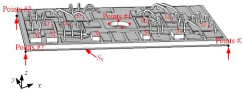
Figure 2 Structure and top view of the IGBT module; d1,d2,…,d6 are FWD diodes, s1, s2,…,s6 are IGBT dies. (a) Structure of IGBT module; (b) Top view
of SK35GD126ET module.
Figure 3 Schematic view and boundary conditions for simulation
Figure 1 Mechanism of temperature gradient change due to solder failure.
Table II
BOUNDARY CONDITIONS OF IGBT SIMULATION.
Item Boundaries
S1 Current Load
[image:4.612.323.560.145.236.2]body. An equivalent heat convection coefficient is applied to the bottom of IGBT module as a boundary condition, so as to simplify the model and reduce the simulation time [23-24]. The corresponding heat transfer coefficient is 2000 W/(m2·K).In the
thermo-mechanical analysis model, and the residual stress/strain from the manufacturing process is assumed to be zero. In addition, each arrow on the bottom of the heat spreader indicates the restrained deformation in the x, y, or z direction, and the edges of hole are fixed to avoid rigid motion.
To more accurate model the thermal characteristic of IGBT
module in different loading conditions, some materials are set with thermal conductivities as temperature dependent [7], especially for silicon, it shows different behaviors at various temperatures. The corresponding thermal properties of materials are listed in Table III and the geometries of each layer in the FEM model are also included. In addition, the thickness of thermal grease is treated as uniform, which is set as 100μm [24], hence the significant impact of thermal grease on thermal stress is counted.
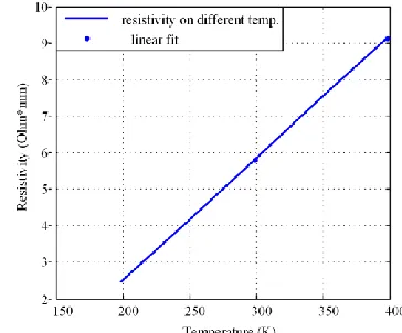
All materials except silicon were considered to have a constant electrical resistivity, as listed in table III. Since the chip possesses higher resistance when the junction temperature increases according to the output characteristic curve[25]. Thus, the electrical resistivity of the chip is temperature dependent. And linear electrical resistivity is adopted to represent the temperature dependent characteristic within the linear region of the current-voltage curve.
For IGBT chip, the pure resistance rce/f is equal to ce/f d r
S
,
where σ is resistivity, d and S are the height and area of chips, which are 0.16mm and 6.8mm*6.8mm, respectively. The value
rce/f can be obtained based on the current-voltage characteristic
curve and it is temperature dependent:
/ ce_ 25/ D_ 25 r, / D
(T
, / D25)
ce f T j T
r
r
K
(8) Consequently, the conductivity σ can be obtained from the resistance rce/f in Eq.(8). The linear electrical resistivity in the [image:5.612.350.532.374.525.2]FEM model is shown in figure 4, the corresponding resistivity of diode can also be calculated according to the parameters in table IV. Additional power dissipation, obtained by multiplying the initial conducting voltage by the collector current, is applied to the chip to compensate for the heat generated by the initial conducting voltage.
All materials, except for the solder are considered to have elastic properties, the solder layer is modelled with linear elastic coupled with visco-plastic material properties. A unified inelastic strain theory called the Anand’s visco-plastic material
model is employed, which accounts for the physical phenomenon of strain-rate and temperature sensitivity, strain hardening or softening characteristics, crystalline texture and its evolution [26]. The material properties of the solder layer are shown in Table V.
where s0 is the initial deformation resistance; Q/R is activation energy/Boltzmann’s constant; A is pre-exponential factor;
is stress multiplier; m0 and ŋ are the strain rate sensitivity of stress and strain rate sensitivity of the saturation value; h0 is the hardening/softening constant; s is the coefficientfor saturation value of deformation resistance and a is the strain rate sensitivity of the hardening/softening.
In order to achieve accurate results and save the simulation time, a multi-level meshing process is executed in the FEM
TABLEIII
TEST CONDITION OF MODULES.
Material (kg·m-3) E(GPa) μ λ W/(m·K) c J/(kg·K) CTE(10-6·K-1) γ (S/m)
L×D(mm) H(mm)
Aluminum 2690 68 0.3 237 900 21 2.7e7 Φ=0.6mm -
Si 2330 162.7 0.28 Temp. 273.15 373.15 473.15
Cond. 168.0 112.0 82.0
700 2.5 Temp. 6.8×6.8 0.15
Ceramic 3890 275 0.22 25 880 6.8 1e-5 52×28.3 0.96
Cu 8960 128.9 0.34 Temp. 401 16.9 1.7e7 52×28.3 0.2
Solder 7400 15.31 0.4 33 234 30.2 9.1e6 6.8×6.8 0.06
grease 1180 - - 2.1 1044 - - 52×28.3 0.012
TABLE IV
OUTPUT PARAMETERS OF IGBT.
Parameters IGBT Diode
Rated voltage VN/V 1200 1200
Rated current IN/A 40 40
Initial conducting voltage drop(25oC) VCE/V 0.9996 1.3456 ON-state resistance(25 oC) rCE/mΩ 20.06 11.95 Temperature coefficient of ON-state
resistance Kr
0.1156e-3 0.332e-4
Figure 4 Temperature-dependent electrical resistivity of IGBT chip.
TABLE V
ANAND’S PARAMETERS DEFINITION.
Parameters s0(MPa) Q/R(K) A (s-1)
Solder 12.41 9400 4.1e6 1.5
m0 h0(MPa) s(MPa) ŋ a
0885-8993 (c) 2016 IEEE. Personal use is permitted, but republication/redistribution requires IEEE permission. See http://www.ieee.org/publications_standards/publications/rights/index.html for more information.
[image:6.612.341.550.130.290.2]simulation. Multi-level meshing means that for the critical layers (bond wires and solder layers), finer meshing is processed rather than other layers like the baseplate and DCB copper. FEM simulations are run in transient mode for 200 s. Within this time the average temperatures of the module are entering into steady-state. FEM is generated as shown in the Fig.5, in which the total number of nodes is 611336 and total number of body elements is 115757.
C. Steady state results
The steady-state temperature profile of the IGBT module is shown in Fig. 6 for the case when all the IGBTs are conducting with 15A current. As it is observed, the maximum temperature is 382K, which lies in the chip s2 as shown in Fig.2.Meanwhile,
the temperature is not symmetrically distributed over the surface of IGBT/Diode chips and there are mutual temperature rises between the chips. The thermal coupling effect would cause temperature rise and change the thermal distribution of chips. So the temperature on each chip is originated from self-heating and thermal coupling effects from the other chips, which is a function of the chip power loss and distance between
chips [7].
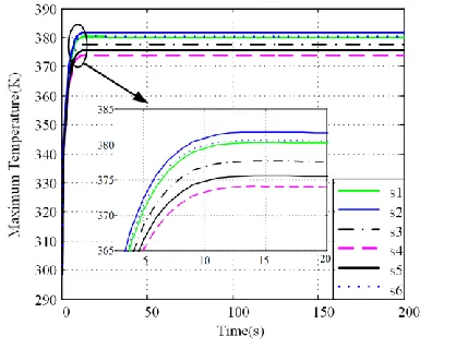
The corresponding maximum temperature for IGBT chips are presented in Fig.7, the maximum temperature for all chips are not the same, the maximum temperature difference reaches 7K and the thermal coupling is higher when chips are closer to each other.
The steady thermal impedance between FEM simulation results and manufacture datasheet are compared in Figure 8, which derives from the average surface temperature and the thermal coupling impedance is also counted. The simulation results agree with the datasheet well, for example the errors for chips x3 are about 4.76% and 4.12%, respectively. The main reason originates from the dependency of material thermal conductivity to temperature. Moreover, the thermal grease has a high impact on temperature distribution, which is more than 0.035K/W in the established FEM model.
D. Effect of power loss on temperature gradient
[image:6.612.75.279.162.241.2]Further simulation models are designed to obtain the temperature gradient distribution under different power loss levels. The IGBT module is fed with different current of 15A, 20A, respectively. The corresponding temperature gradient distribution are shown in Fig.9, in which the bond wires are hidden. It can be seen that the temperature gradient increases with current. For example, when the current increases by 5A, the temperature gradient increases from 56.83K/cm to
Figure 5 3-D finite element mesh of IGBT module model.
(a)
[image:6.612.78.274.401.714.2](b)
Figure 6 Temperature distribution of IGBT module. (a) Three-dimension view; (b) Top view.
[image:6.612.323.557.432.613.2]Figure 7 Maximum temperature for all IGBT chips
83.5K/cm and the power loss increases by about 10.2W. The trend agrees with the previous analysis, which is the higher temperature gradient reflects the larger power loss.
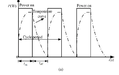
Temperature gradient for power cycling condition is also carried out. Fig.10(a) outlines the schematic of a cyclic power load [27]. The cycle period is 20 s: 10s for power on and 10s for power off. The temperature gradient of monitoring point in Fig.9(b) is shown in Fig.10(b). The maximum temperature gradient is 82.53K/cm when t=200s and would decrease to zero when the power is off. It can be also observed that the temperature gradient varies with power loss, with the same cycle period of 20s, which coincides with the steady state simulation results.
Several more simulations are designed to obtain the relationship between temperature gradient and power loss levels as shown in Fig.11. Fig.11(a) represents the steady-state temperature gradient for single chip geometry along the dialogue line, in which the reference point is set as the corner of chip. The same material and dimension structure for the above FEM model are used. Results in Fig.11(a) indicate that larger power loss will cause larger temperature gradient. Fig.11(b) displays the temperature gradient for the above module. It is obvious that the temperature gradient is directly proportional
(a)
[image:7.612.340.555.53.219.2]
(b) Figure 9 Temperature gradient of IGBT modules with different current.
(a) I=15A; (b) I=20A.
(a)
(a)
(b)
Figure 11 Variation of temperature gradient with power loss. (a)Temperature gradient for single chip case; (b) Temperature gradient
for multi-chips case.
[image:7.612.65.286.88.415.2](b)
[image:7.612.330.530.248.581.2] [image:7.612.55.287.556.703.2]0885-8993 (c) 2016 IEEE. Personal use is permitted, but republication/redistribution requires IEEE permission. See http://www.ieee.org/publications_standards/publications/rights/index.html for more information.
with power loss in all cases. This result agrees with the analysis made in section II. According to Fourier’s law, temperature gradient depends on heat flux and power loss[22,28-29], while the power loss increases with the thermal resistance. Therefore, once solder fatigue occurs, the thermal resistance will increase, finally the power loss and temperature gradient will increase.
IV. CHARACTERISTIC OF TEMPERATURE GRADIENT SOLDER
FAILURES A. Steady-state results for solder fatigue
It can be concluded from section III that the temperature gradient increases with thermal resistance, which is further investigated in this Section. The study of individual die-attach solder fatigue on temperature gradient is carried out by creating a vacuum layer in the die-attach solder. In the simulation, thermal conductivity λ=1.01W/(m·K), thickness of fatigue layer d= 0.01mm and fatigue area A= 6.8mm×6.8mm, so the calculated thermal resistance △Rth=d/(λ·A)=0.27oC /W, which
is about 25.7% of the manufacture value [13]. The temperature gradient distribution Tg_j corresponding to △Rth is shown in
Fig.12, it increases from 56.83K/cm to 66.11K/cm, achieving 16.33%, with the same computational conditions in Fig.6.
In addition, the temperature gradient and related power losses with/without failures are analyzed, and Table VI lists the steady-state temperature gradient and power losses obtained from simulation. The temperature gradient Tg_j of the IGBT
increases by about 10K/cm with the solder fatigue, while the devices in the module dissipate more power about 0.19W for individual IGBT chip.
The above conclusion is confirmed in another simulation, in which die-attach solder fatigue occurs in all chips. Fig.13 shows the result of 20% increased Rth when I=20A. As it is
observed, the temperature gradient increases with thermal resistance, about 13K/cm. The trend agrees with the previous observation, as when the thermal impedance is higher and the
power loss is larger, the temperature gradient will be larger.
B. Temperature gradient distribution for solder void
The voids are almost inevitable in solder layer during manufacturing, this would drop the performance of heat dissipation of IGBT module and cause progressive further degradation. Thus, impact of void on temperature gradient is discussed in the part. In the paper, the studied through-thickness voids are assumed as regular cylinder [26,30]. Since in the qualification test, the die attach requires a corner void should not be bigger than 10% of the total void area [26]. Hence, 10% void area was chosen for this study as a level of interest. The through-thickness solder voids are of radius 1.2 mm and 0.06 mm deep in the solder layer.
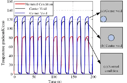
The study on effect of voids location on the temperature gradient is carried out. Representative voids are situated at different horizontal positions in the solder layer as shown in Fig.14, while the solder layer without void is a reference. The temperature gradient of different voids are compared in Fig.14. As it can be seen, the temperature gradient varies with power loss, with the same cyclic period. On the other hand, the increased temperature gradient depends on the location of void. The corner void results in the greatest magnitude change, about 44.7K/cm, while that for center void is 33.4K/cm. For the through void cases, the corner voids are more detrimental to the reliability of the solder and appears to have a more severe influence on solder layer, which agrees with previous research results[30].
[image:8.612.347.530.74.223.2]
Figure 12 Temperature gradient of chips x3 for a 25.7% increase of Rth when I=15A.
TABLE VI
EFFECT OF EMULATED FAILURE ON TEMPERATURE GRADIENT. Ta (K) Tj_ave(K) Tg_j(K) Pj_ave(W)
Without failure 297.45 373.33 56.83 20.12 With failure 297.45 379.26 66.11 20.31
Figure 13 Temperature gradient of chips x3 for an overall 20%increase of Rth when I=20A.
[image:8.612.339.551.580.719.2]
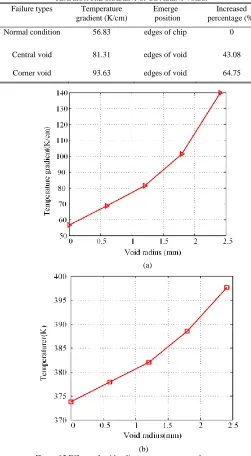
More simulation models are conducted to study the effect of voids on temperature gradient. Steady-state temperature gradient under different voids is summarized in Table VII. It can be seen that the maximum temperature gradient appears in failure region, which helps to detect the defects. In addition, the increased temperature gradient of corner void is larger than that of center void, about 43% and 65%, respectively. This agrees with the power cycling simulation results, so the corner void has more severe influence on solder layer.
The interaction between center void radius and temperature gradient, temperature, are shown in Fig.15. It is obvious that temperature gradient increases with the void radius. In Fig.15(a), the temperature gradient increases by about 85K/cm when void area increases by about 39%. Fig.15(b) shows that the temperature increases with void percentage and has a
similar tendency with temperature gradient. While the rate of change for temperature and temperature gradient are 6.68% and 146.35% when void radius increases to r=2.4mm, respectively.
C. Simulation results of solder delamination
Solder delamination is another form of solder fatigue, which often starts form the boundary of solder and expands toward to center [8]. Consequently, the delamination case is discussed and the solder fatigue is modelled by creating a 15 μm-thick vacuum “delamination” layer in the die-attach solder layer. Two simplified models derived from the observed results in reference [31] are investigated. The corresponding temperature gradient when I=15A is displayed in Fig.16. As it can be seen, the temperature gradient increases with thermal resistance and larger temperature gradient occurs in the delamination region. In addition, the temperature gradient for enclosed boundary delamination is lower than inner segment delamination, which are about 71K/cm and 109K/cm, respectively.
Impact of delamination rate on temperature gradient is also discussed, as shown in Fig.17. It is observed that temperature gradient increases rapidly as the delamination propagates further, mainly due to the reduced effective heat dissipation region. Referring to Fig.17, the temperature gradient increases by over 70K/cm when delamination rate increases from 10% to 40%, while it increases only about 10K/cm when the delamination rate is less than 10 %.
(a)
[image:9.612.39.290.179.635.2](b)
Figure 15 Effects of void radius on temperature and temperature gradient. (a) Temperature gradient; (b) Temperature.
TABLE VII
TEMPERATURE GRADIENT OF DIFFERENT VOIDS. Failure types Temperature
gradient (K/cm)
Emerge position
Increased percentage (%)
Normal condition 56.83 edges of chip 0
Central void 81.31 edges of void 43.08
Corner void 93.63 edges of void 64.75
(a)
[image:9.612.342.561.267.592.2]
(b)
0885-8993 (c) 2016 IEEE. Personal use is permitted, but republication/redistribution requires IEEE permission. See http://www.ieee.org/publications_standards/publications/rights/index.html for more information.
V. EXPERIMENTAL SETUP AND DISCUSSION A. Experiment rig
The circuit configuration of test converter and the corresponding test platform for temperature gradient measurement are shown in Fig.18 The half-bridge IGBT module and single phase two-level neutral point clamped H typed converter are used. A high-frequency infrared thermal camera is used to measure the surface temperature of an opened IGBT module during the operation of converter. The detailed parameters of the experimental setup are shown in table VIII. To avoid the effect of control strategy on temperature measuring, the open-loop control method is used. The LC filter is also used to reduce noise. The converter is loaded by pure resistance and DC source is used to feed the converter with constant DC voltage, thereby the current loading of device can be adjusted by changing the modulation index.
The IGBT module is attached on a heat sink through thermal grease to improve the thermal contact and ensure effective heat dissipation. As there are two holes on the top side of the power module, it is possible to fix the module with screws on a heat sink and forced wind cooling is used in the experiment. The FLIR SC7000 infrared camera (IR) is used to measure the temperature. The measurements are done in the middle wavelength range (1.5-5μm) with InSb matrix sensors of 320×256 active cells. All IR measurements are performed with a 400Hz sampling frequency. The IR temperature measurements are conducted by controlling the surface emissivity with a black paint solution. In addition, a K type sensor thermocouple is attached below the chip center of the diode and IGBT to monitor case-to-ambient temperature.
The thermo-sensitive electrical parameters (TSEPs) of a collector-emitter voltage (Vce) under a low current (i.e.100mA)
is chosen to obtain the junction temperature [32]. The temperature measurement is carried out in the environmental chamber. The temperature of the chamber is increased from 20°C to 120°C, and the collector-emitter voltage (Vce) is
measured when the temperature reaches steady state. Fig.19(a) shows the variation of the measured voltage as a function of temperature. Function fitting is used to obtain the dependence parameters and the relationship between Vce and temperature, which can be described by Eq. (9). It is clearly that the voltage decreases linearly with temperature.
[image:10.612.360.517.49.265.2]
(a)
[image:10.612.59.263.66.236.2]Figure 17 Relationship between solder delamination rate and temperature gradient.
TABLE VIII
PARAMETERS OF EXPERIMENTAL SETUP. DC bus voltage Vdc 130V DC capacitance C1 3300μF Switching frequency fsw 4kHz
Filter inductance Lf 2mH Filter capacitance C2 20µF Load resistance RL 5Ω
IGBT module 1200V/50A Infrared camera SC7000
(b)
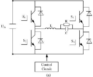
Figure 18 Diagram of electrical topology and configuration of experimental setup. (a)Circuit Topology Diagram;(b) Experimental.
[image:10.612.73.264.489.648.2]_100
461 303.7
j ce mA
T V (9)
To verify the reliability of method in the paper, comparison of TSP measurement results and infrared camera (IR) method results is made simultaneously, as shown in Fig.19(b). Good agreement is observed over the temperature rise test duration, with error less than 0.6°С. Therefore, the temperature measurement method can be used and the accuracy meets the design requirement.
B. Temperature gradient results
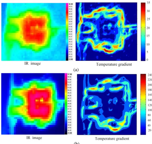
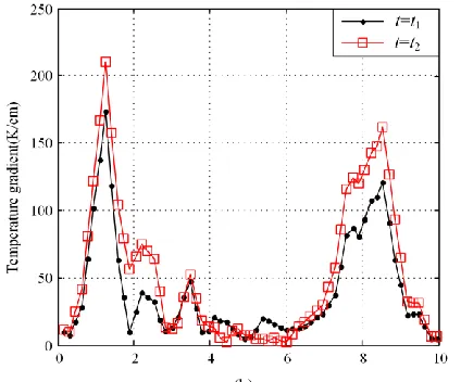
As discussed in above sections, temperature gradient increases with power loss, in other words, the temperature gradient varies with different operation conditions. Temperature gradient of inverter condition when output frequency f=0.1Hz, output current I=5.5, I= 22A, respectively, are investigated. Fig.20 shows the temperature gradient distribution for peak current condition. The corresponding temperature gradient are about 35K/cm and 223K/cm, while the temperature are about 307.05K and 329.15K, respectively. On the other hand, the increased temperature gradient (187K/cm) is much higher than the temperature (22K) when the current increases by 16.5A. This agrees with the above conclusion that the larger power loss would cause larger temperature gradient fluctuation.
To show the experiment results quantitatively, Fig. 21 shows the temperature gradient of different locations when I=22A. It is obvious that the temperature gradient variation is different for different heating phases, when the current is higher, the temperature gradient is also larger. In addition, the function shape for different heating phases is also different, the correlation of that two curves becomes weaker and the maximum vertical temperature gradient change is about 45K/cm. It is thus can be concluded that temperature gradient can track the change of operation condition and power loss well, hence it can be used to condition estimation or design study.
(a)
(b)
Figure 19 Temperature calibration and comparison results; (a) Sensitivity calibration result; (b) Comparison of Tj between IR and Vce
(a)
[image:11.612.315.573.201.445.2](b)
Figure 20 Temperature and temperature gradient distribution for different conditions. (a) Temperature and temperature gradient distribution when I=5.5A;(b) Temperature and temperature gradient distribution when I=22A.
0885-8993 (c) 2016 IEEE. Personal use is permitted, but republication/redistribution requires IEEE permission. See http://www.ieee.org/publications_standards/publications/rights/index.html for more information.
Further validation tests have been carried out, and temperature gradient distribution between new and aged IGBT module is studied. Power cycling tests are designed to obtain the process of power modules failure. The test rig and main electrical circuit are shown in Fig. 22. In the aging test, four IGBTs are connected in series to ensure that all chips are working under the same cycling current which is controlled by using the remote current mode of power supply. The control strategy of the rig keeps the swing of case temperature at a constant value. A 100 mA current source is connected through all modules which are permanently gated on. In this setup, a heating up phase is initiated by closing a heating control switch. When the heating control switch turns off, the IGBTs are sent into a cooling phase. The IGBT modules are simultaneously heated by current load, in order to set the temperature difference between Tjmax and Tjmin(ΔTj) to the desired value.
Meanwhile, the collector-emitter voltage Vce is used to obtain
the temperature and K type thermocouples are selected to measure the case temperature. The junction temperature (Tjmax)
of each IGBT module is obtained by measuring the corresponding collector-emitter voltage Vce caused by the
100mA current when heating control switch is off. During cooling, the current going through the IGBTs keeps at 100 mA, therefore the measurements of Vce will continually indicate the
decaying junction temperature. Since the sensing current (100mA) is much smaller than the controlled heating current (e.g. 60A), it contributes little to the heating. The module thermal resistance Rth is obtained at the beginning of each
cooling phase from the junction-above-case temperature and the power loss which can be calculated from voltage and current. The minimum junction temperature Tjmin is obtained in
a similar way at the end of the cooling phase. Tjmax and Tjmin
define the stress level ΔTj which can be adjusted by: the duty
cycle and period of the heating control switch. Device degradation is monitored at the end of each heating phase by comparing with the measured Vce and thermal resistance of the
module Rth with their initial values. An inductor is connected in
the circuit to limit the current overshoot when the heating control switch turns on.
Reference [32] shows that cracks occur at the die attach solder layer when ΔTj is not more than 120oC. Therefore, test
condition of modules is set as ΔTj=120oC, Tm=100oC, the
heating time and cooling time are 30s and 20s, respectively in each cycle. Thermal resistance Rth is normalized with respect to
its initial value for the new module to reduce the calculation error. Collector-emitter voltage Vce is also plotted to make sure
that a bond wire joint has not occurred, hence the main aging-to-failure mechanism under investigation is indeed the die-attach solder fatigue. The aging tests are finished once the studied parameters close to the set failure threshold, which are increased by 50% and 20% for Rth and Vce [32].Fig.23 shows
the test results. It is obviously that, the measured Vce almost
doesn’t change and thermal resistance increases faster. The die-attach solder mostly degrades before bond wire degrades. This indicates that the solder fatigue is the dominant failure mechanism in the designed test conditions for the selected IGBT modules.
(a)
[image:12.612.66.278.62.238.2]
(b)
Figure 22 Power cycling test rig and main electrical circuit. (a)Test rig; (b)Main circuit.
(b)
Figure 21 Temperature gradient for large power loss case.(a) Temperature gradient along horizontal center line;(b) Temperature gradient along
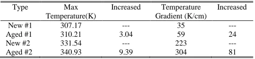
[image:12.612.317.566.123.441.2]Temperature gradient of aged IGBT module under the same condition in Fig.20 is shown in Fig. 24. Compared with the new IGBT, it is found that even for small current condition, increased temperature gradient is more than 24K/cm. The compared and summarized temperature gradient and temperature results are listed in table IX.
The increased temperature is about 3.04K and the increased temperature gradient is over 24K/cm when I=5.5A, which is enough for reliable detection. The similar principle can also be observed in I=22A case, the temperature gradient increases about 9.4K and 81K/cm. Thereby, the temperature gradient can track the thermal resistance increase, as well as the power loss.
In addition, the increased temperature gradient between new and aged IGBT module are about 68.57% and 36.32%, respectively, while the temperature increases by 1% and 2.86%, respectively. The change of temperature gradient is much greater than that of temperature.
[image:13.612.70.265.61.236.2]To further discuss the difference of temperature gradient between new and aged IGBT module, temperature gradient for different locations are given in Fig.25. The maximum temperature gradient difference between aged IGBT and new IGBT module when I=22A is over 70K/cm and that for I=5.5A is less than 20K/cm. It means the temperature gradient change also depends on current, as well as power loss in both new and aged IGBT module.
Figure 23 Change of normalized Rth and Vce
(a)
(b)
[image:13.612.315.578.145.206.2]Figure 24 Temperature gradient of aged IGBT module. (a) Temperature gradient when I=5.5A; (b) Temperature gradient when I=22A
TABLE IX
Temperature and temperature gradient for both new and aged IGBT module
Type Max
Temperature(K)
Increased Temperature Gradient (K/cm)
Increased
New #1 307.17 --- 35 ---
Aged #1 310.21 3.04 59 24
New #2 331.54 --- 223 ---
Aged #2 340.93 9.39 304 81
(a)
(b)
Figure 25 Comparison of temperature gradient between new and aged IGBT modules.(a) Horizontal temperature gradient for center line;(b)
[image:13.612.82.274.315.627.2] [image:13.612.313.567.316.700.2]0885-8993 (c) 2016 IEEE. Personal use is permitted, but republication/redistribution requires IEEE permission. See http://www.ieee.org/publications_standards/publications/rights/index.html for more information.
Temperature gradient of multi-chips is also investigated, the corresponding temperature gradient between new and aged IGBT module is shown in Fig.26. It can be seen that the maximum temperature increases about 3K and temperature gradient increases by about 25K/cm when solder fatigue occurs. The corresponding rate of change of temperature and temperature gradient are 8.33% and 55.56%, respectively.
The same principle can also be observed in Fig.27, and the maximum changed temperature gradient in all cases is over 30K/cm. The increase in the thermal resistance increase would cause temperature gradient increases. Therefore, the proposed method could be suitably to support condition estimation and design study. It is expected the method can be extended to other modules or devices, such as SiC module or other electrical devices.
C. Influence of electric parameters
In reality, power loss of IGBT module depends on many factors, such as dc side voltage Vdc, modulation index m, and
output frequency f and so on. In this section, the influences caused by dc side voltage Vdc and output frequency f were
investigated.
Fig.28 shows the junction temperature fluctuation of different voltages. It is observed that junction temperature increases with dc side voltage Vdc, and the temperature
fluctuation is over 17K when dc side voltage Vdc=131V. The
[image:14.612.335.559.54.229.2]corresponding temperature gradient distribution is shown in Fig.29, as it can be seen, the temperature gradient increases by about 184K/cm when the voltage Vdc increases from 42V to
131V. This indicates that the temperature gradient increases with power loss, because the power loss increases with Vdc in an
[image:14.612.52.293.148.359.2]exponential form approximately [24].
Figure 28 Temperature fluctuation of IGBT for different loadings.
(a)
Figure 26 Temperature and temperature gradient distribution of new and aged IGBT module.(a) Temperature of new and aged IGBT;(b)
Temperature gradient of new and aged IGBT.
(a)
(b)
Figure 27 Comparison of temperature gradient between new and aged IGBT modules.(a) Horizontal temperature gradient of central line;(b)
[image:14.612.322.556.353.547.2] [image:14.612.74.274.495.678.2]It is known that the temperature increases with the decreasing of output frequency. While the power loss increases with temperature, hence, the power loss varies with output frequency. Serveral experiment tests were done to explore the infuence of output frequency on temperature gradient, as shown in Fig.30. Fig.30(a)-(c) shows that the temperrature gradient decreases about 50K/cm, when f increases from 5Hz to 50Hz. Hence, influence of output frequency f should be considered when the method is applied into condition estimation system.
VI. CONCLUSIONS
The paper presents a temperature gradient based method for device state evaluation, and the insulated Gated Bipolar Transistor (IGBT) modules is taken as an example investigation. The method is used to indicate the increase of thermal resistance and power loss of IGBT module caused by solder fatigue. The method is validated against analytical analysis, FEM simulation and experimental results. It is confirmed that the increased thermal resistance and power loss of IGBT modules would cause increase of the temperature gradient. The results have shown that a 20% increase of the thermal resistance Rth gives a temperature gradient rise about
10K/cm for the inverter system. Results from localized solder fatigue, including voids and delamination indicate that temperature gradient can track change of power loss and has be better sensitivity compared with temperature, and it can determine the location of defects. Experimental results also verify the conclusion. It is hoped that the study would help developing more accurate condition evaluation and resulting in a more effective support for qualification test.
REFERENCES
[1] Alex, Revell Alistair, Iacovides Hector, et al, “Numerical prediction of local hot-spot phenomena in transformer windings,” Applied Thermal Engineering, vol.36, no.1, pp. 96-105,2012.
[2] Shuguang Liu, Jingcui Chen, Yongbo Qu, “Study on optical fiber temperature-sensing technique for vacuum circuit breaker contactor,” International Conference on Electrical and Control Engineering (ICECE), Yichang, 2011,pp.1299-1302.
[3] Po-Chien Chou, Stone Cheng, Design and characterization of a 200 V, 45 A all-GaN HEMT-based power module, Applied Thermal Engineering, vol.61. pp.20-27,2013.
[4] A. Hamidi, G. Coquery, R. Lallemand and P. Vales, Temperature measurements and thermal modeling of high power IGBT multichip modules for reliability investigations in traction applications, Microelectronic Reliability, vol.38,no.6,pp. 1353–1359, 1998.
[5] N. Shammas, “Present problems of power module packaging technology,” Microelectron Reliability, vol.43. no. 4, pp.519-527,2003. [6] H. Wang, M. Liserre, F. Blaabjerg, “Toward Reliable Power
Electronics:Challenges, Design Tools, and Opportunities,” IEEE Ind. Electron.Mag., vol. 7, pp.17-26, 2013.
[7] Amir Sajjad Bahmann, Ke Ma, Frede Blaabjerg. A novel 3D thermal impedance model for high power modules considering multi-layer thermal coupling and different heating/cooling conditions, IEEE Applied (a) (b)
[image:15.612.333.554.50.225.2](c) (d)
Figure 29 Influence of dc side voltage on temperature gradient of IGBT; (a) 42V; (b) 72V; (c) 101V; (d)131V.
(c)
Figure 30 Temperature gradient for different output frequency.(a) 5Hz;(b) 10Hz;(c)50Hz;
(a)
[image:15.612.46.300.51.275.2]0885-8993 (c) 2016 IEEE. Personal use is permitted, but republication/redistribution requires IEEE permission. See http://www.ieee.org/publications_standards/publications/rights/index.html for more information. Power Electronics Conference and Exposition (APEC), Charlotte,
2015,pp.1209 - 1215.
[8] Ji, B.; Pickert, V.; Cao, W.; Zahawi, B.; , “In Situ Diagnostics and Prognostics of Solder Fatigue in IGBT Modules for Electric Vehicle Drives,” Power Electronics, IEEE Transactions on, vol.30, no.3, pp. 1535-1543, 2015.
[9] Li Yang, Pearl A. Agyakwa, and C. Mark Johnson.Physics-of-Failure Lifetime Prediction Models for Wire Bond Interconnects in Power Electronic Modules, IEEE TRANSACTIONS ON DEVICE AND MATERIALS RELIABILITY, vol. 13, no. 1,pp.9-17,2013.
[10] I.R.sWAN,A.T.Bryant,N.-A. Parker-Allotey. 3-D thermal simulation of power module packaging. Energy Conversion Congress and Exposition, San Jose,2009. pp.1247-1254.
[11] A. Watanabe and I. Omura, “Real-time failure imaging system under power stress for power semiconductors using scanning acoustic tomography (SAT),” Microelectron. Rel., vol. 52, no. 9/10, pp. 2081–2086, 2012.
[12] K. Li, G. Tian, L. Cheng, A. Yin, W. Cao, and S. Crichton, “State detection of bond wires in IGBT modules using eddy current pulsed thermography,” IEEE Trans. Power Electron., vol. 29, no. 9, pp.5000-5009, 2014.
[13] Dawei Xiang, Li Ran. “Monitoring Solder Fatigue in a Power Module Using Case-Above-Ambient Temperature Rise”. IEEE Transactions on industry applications,vol,47,no,6, pp.2578-2590,2011.
[14] D.Xiang,L.Ran,P,Tavner,et. “Condition Monitoring Power Module Solder Fatigue Using Inverter Harmonic Identification, ”.IEEE Transactions on Power Electronic,vol,27,no,1,pp.235-247,2011. [15] Zhou Luowei,Zhou Shengqi,Sun Pengju. Diagnostic Method for Internal
Defects of IGBTs Base on Stray Parameter Identification. Transactions of China Electro technical Society, vol.27.no.5, pp.156-163,2012. [16] Zhou, S.; Zhou, L.; Sun, P.; , Monitoring Potential Defects in an IGBT
Module Based on Dynamic Changes of the Gate Current, Power Electronics, IEEE Transactions on, vol.28, no.3, pp.1479-1487, 2013. [17] A. Bryant, S. Y. Yang, P. Mawby, D. W. Xiang, L. Ran, P. Tavner, and P.
R. Palmer, “Investigation into IGBT dV/dt during turn-off and its temperature dependence,” IEEE Trans. Power Electron., vol. 26, no. 10, pp. 3019–3031, 2011.
[18] Nishad Patil,Dignanta Das,Kai Goebel,etal. “Identification of failure precursor parameters for Insulated Gate Bipolar Transistors(IGBTs),” International Conference on PHM, Denvor, 2008,pp.271-276.
[19] Josef Lutz, Uwe Scheuermann. Semiconductor Power Devices: physics, characteristics, reliability, Springer(2011):pp360-362.
[20] R.HOCINE,M.A.BOUDGHENE STAMBOULI, A. SAODANE.A three-dimensional TLM simulation method for thermal effect in high power insulated gate bipolar transistors, Semiconductor Thermal Measurement and Management, 2002. Eighteenth Annual IEEE Symposium, San Jose, pp.99-104.
[21] Assis A K T,Rodrigues Jr. W A,Mania A J. The Electric Field Outside a Stationary Resistive Wire Carrying a Constant Current. Foundations of Physics,vol.29,no.5,pp.729-753,1999.
[22] Larisa Mariut. Temperature gradient effect of partial discharge activity-modelling and simulation, Applied and Theoretical Electricity (ICATE), 2012 International Conference on, Craiova ,2012, pp.1-8. [23] J. H. Lienhard IV and J. H. Lienhard V, “A heat transfer handbook,”
Cambridge: Phlogiston press, Third edition, 2003.
[24] Ke Ma, Amir Sajjad Bahman, Szymon Beczkowski. Complete loss and thermal model of power semiconductors including device rating information. Power Electronics, IEEE Transactions on, vol.30, no.5, pp.2556-2569, 2015.
[25] Seimkron IGBT Module datasheet,SK35GD126ET[Online].Available:
http://www.semikron.com/products/data/cur/assets/.
[26] Kenny C. Otiaba, M.I. Okereke, R.S. Bhatti, Numerical assessment of the effect of void morphology on thermo-mechanical performance of solder thermal interface material, Applied Thermal Engineering, vol.64. no.2,pp. 51-63, 2014.
[27] T.Y,Hung ,L.L.Liao, C.C.Wang. Life prediction of high cycle fatigue in aluminum bonding wires under power cycling test. IEEE Transactions on Device and Material Reliability,vol.14.no.1,pp.484 - 492,2013. [28] Tao Wenquan, Heat Transfer.XiAn:XiAn JiaoTong university
press,2001,pp.6-25.
[29] Mingjing,Zhai, Menjie,Guo. Effect of high-temperature solder void on heat dissipation performance of smart power module, 2011 Internal conference on electronics and optoelectronics,Dalian,2011,pp.404-406.
[30] XieXinpeng, Bi Xiangdong, Hu Jun. Effects of Voids on Thermal Reliability in Power Chip Die Attachment Solder Layer. Semiconductor Technology, vol,34,no,10, pp.960-964, 2009.
[31] O.Schilling.M.Schäfer, K.Mainka. Power cycling testing and FE modelling focused on Al wire bond fatigue in high power IGBT modules. Microelectronics Reliability,vol.52,no.9.pp.2347-2352,2012.
[32] Hui Huang; Mawby, P.A.; , A Lifetime Estimation Technique for Voltage Source Inverters, Power Electronics, IEEE Transactions on, vol.28, no.8, pp. 4113-4119, 2013.
Bing Gao received the B.E. degree from School of Electrical Engineering, Chongqing University, Chongqing, China, in 2011. He is currently working towards a Ph.D. degree in the School of Electrical Engineering, Chongqing University, Chongqing, China. His research interests include the reliability of power modules, the multi-physics coupling field calculation for power electronics and the development of condition monitoring methods for power electronic converters.
Fan Yang received the PhD degree in school of electrical engineering, Chongqing University, China in 2008. He was a visiting Scholar at Oklahoma State University, Oklahoma, the USA 2012. Now he is a professor in electrical engineering of Chongqing University. His research of interests includes: condition monitoring methods for electrical apparatus, the multi-physics coupling field calculation for renewable devices.
Minyou Chen (M’05-SM’14) received the M.Sc. degree in Control Theory and Engineering from Chongqing University, China, in 1987, and the Ph.D. degree in control engineering from the University of Sheffield, Sheffield, the UK, in 1998. He is currently a Full Professor at Chongqing University. He is the author or coauthor of more than 180 papers. His research interests include intelligent modeling and control, reliability of power modules, micro-grid control, state monitoring in power distribution systems.