and Model a Pipeline and More Pipelining
Illustrations
This CD section covers hardware decription langauges and then a dozen examples
of pipeline diagrams, starting on page 4.12-16.
As mentioned in Appendix C, Verilog can describe proces sors for simulation
or with the intention that the Verilog specifi cation be synthesized. To achieve
acceptable synthesis results in size and speed, a behavioral specifi cation intended
for synthesis must carefully delineate the highly combinational portions of the
design, such as a datapath, from the control. The datapath can then be synthesized
using available libraries. A Verilog specifi ca tion intended for synthesis is usually
longer and more complex.
We start with a behavioral model of the 5-stage pipeline. To illustrate the
dichot-omy between behavioral and synthesizeable designs, we then give two Verilog
descriptions of a multiple-cycle-per-instruction MIPS processor: one intended
solely for simulations and one suitable for synthesis.
Using Verilog for Behavioral Specifi cation with
Simulation for the 5-Stage Pipeline
Figure 4.12.1 shows a Verilog behavioral description of the pipeline that handles
ALU instructions as well as loads and stores. It does not accommodate branches
(even incorrectly!), which we postpone including until later in the chapter.
Because Verilog lacks the ability to defi ne registers with named fi elds such as
structures in C, we use several independent registers for each pipeline register. We
name these registers with a prefi x using the same convention; hence, IFIDIR is the
IR portion of the IFID pipeline register.
This version is a behavioral description not intended for syn thesis. Instructions
take the same number of clock cycles as our hardware design, but the control
is done in a simpler fashion by repeatedly decoding fi elds of the instruction in
each pipe stage. Because of this difference, the instruction register (IR) is needed
throughout the pipeline, and the entire IR is passed from pipe stage to pipe stage.
As you read the Verilog descriptions in this chapter, remember that the actions in
the
always
block all occur in parallel on every clock cycle. Since there are no
block-ing assignments, the order of the events within the
always
block is arbitrary.
module CPU (clock); // Instruction opcodes
parameter LW = 6’b100011, SW = 6’b101011, BEQ = 6’b000100, no-op = 32’b00000_100000, ALUop = 6’b0; input clock;
reg[31:0] PC, Regs[0:31], IMemory[0:1023], DMemory[0:1023], // separate memories IFIDIR, IDEXA, IDEXB, IDEXIR, EXMEMIR, EXMEMB, // pipeline registers EXMEMALUOut, MEMWBValue, MEMWBIR; // pipeline registers
wire [4:0] IDEXrs, IDEXrt, EXMEMrd, MEMWBrd, MEMWBrt; // Access register fi elds wire [5:0] EXMEMop, MEMWBop, IDEXop; // Access opcodes
wire [31:0] Ain, Bin; // the ALU inputs
// These assignments defi ne fi elds from the pipeline registers assign IDEXrs = IDEXIR[25:21]; // rs fi eld
assign IDEXrt = IDEXIR[20:16]; // rt fi eld assign EXMEMrd = EXMEMIR[15:11]; // rd fi eld assign MEMWBrd = MEMWBIR[15:11]; //rd fi eld
assign MEMWBrt = MEMWBIR[20:16]; //rt fi eld--used for loads assign EXMEMop = EXMEMIR[31:26]; // the opcode
assign MEMWBop = MEMWBIR[31:26]; // the opcode assign IDEXop = IDEXIR[31:26]; // the opcode
// Inputs to the ALU come directly from the ID/EX pipeline registers assign Ain = IDEXA;
assign Bin = IDEXB;
reg [5:0] i; //used to initialize registers initial begin
PC = 0;
IFIDIR = no-op; IDEXIR = no-op; EXMEMIR = no-op; MEMWBIR = no-op; // put no-ops in pipeline registers for (i=0;i<=31;i=i+1) Regs[i] = i; //initialize registers--just so they aren’t cares
end
always @ (posedge clock) begin
// Remember that ALL these actions happen every pipe stage and with the use of <= they happen in parallel! // fi rst instruction in the pipeline is being fetched
IFIDIR <= IMemory[PC>>2]; PC <= PC + 4;
end // Fetch & increment PC
// second instruction in pipeline is fetching registers
IDEXA <= Regs[IFIDIR[25:21]]; IDEXB <= Regs[IFIDIR[20:16]]; // get two registers
IDEXIR <= IFIDIR; //pass along IR--can happen anywhere, since this affects next stage only! // third instruction is doing address calculation or ALU operation
if ((IDEXop==LW) |(IDEXop==SW)) // address calculation EXMEMALUOut <= IDEXA +{{16{IDEXIR[15]}}, IDEXIR[15:0]};
else if (IDEXop==ALUop) case (IDEXIR[5:0]) //case for the various R-type instructions 32: EXMEMALUOut <= Ain + Bin; //add operation
default: ; //other R-type operations: subtract, SLT, etc. endcase
Implementing Forwarding in Verilog
To further extend the Verilog model, Figure 4.12.2 shows the addition of
forward-ing logic for the case when the source instruction is an ALU instruction and the
source. Neither load stalls nor branches are handled; we will add these shortly. The
changes from the earlier Verilog description are highlighted.
Someone has proposed moving the write for a result from an ALU instruction
from the WB to the MEM stage, pointing out that this would reduce the maximum
length of forwards from an ALU instruction by one cycle. Which of the following
are accurate rea sons
not
to consider such a change?
1. It would not actually change the forwarding logic, so it has no advantage.
2. It is impossible to implement this change under any circum stance since the
write for the ALU result must stay in the same pipe stage as the write for a
load result.
3. Moving the write for ALU instructions would create the possibility of writes
occurring from two different instruc tions during the same clock cycle. Either
an extra write port would be required on the register fi le or a structural
hazard would be created.
4. The result of an ALU instruction is not available in time to do the write
during MEM.
Check
Yourself
EXMEMIR <= IDEXIR; EXMEMB <= IDEXB; //pass along the IR & B register//Mem stage of pipeline
if (EXMEMop==ALUop) MEMWBValue <= EXMEMALUOut; //pass along ALU result else if (EXMEMop == LW) MEMWBValue <= DMemory[EXMEMALUOut>>2]; else if (EXMEMop == SW) DMemory[EXMEMALUOut>>2] <=EXMEMB; //store MEMWBIR <= EXMEMIR; //pass along IR
// the WB stage
if ((MEMWBop==ALUop) & (MEMWBrd != 0)) // update registers if ALU operation and destination not 0 Regs[MEMWBrd] <= MEMWBValue; // ALU operation
else if ((EXMEMop == LW)& (MEMWBrt != 0)) // Update registers if load and destination not 0 Regs[MEMWBrt] <= MEMWBValue;
end endmodule
module CPU (clock);
parameter LW = 6’b100011, SW = 6’b101011, BEQ = 6’b000100, no-op = 32’b00000_100000, ALUop = 6’b0; input clock;
reg[31:0] PC, Regs[0:31], IMemory[0:1023], DMemory[0:1023], // separate memories IFIDIR, IDEXA, IDEXB, IDEXIR, EXMEMIR, EXMEMB, // pipeline registers EXMEMALUOut, MEMWBValue, MEMWBIR; // pipeline registers
wire [4:0] IDEXrs, IDEXrt, EXMEMrd, MEMWBrd, MEMWBrt; //hold register fi elds wire [5:0] EXMEMop, MEMWBop, IDEXop; Hold opcodes
wire [31:0] Ain, Bin; // declare the bypass signals
wire bypassAfromMEM, bypassAfromALUinWB,bypassBfromMEM, bypassBfromALUinWB, bypassAfromLWinWB, bypassBfromLWinWB;
assign IDEXrs = IDEXIR[25:21]; assign IDEXrt = IDEXIR[15:11]; assign EXMEMrd = EXMEMIR[15:11]; assign MEMWBrd = MEMWBIR[20:16]; assign EXMEMop = EXMEMIR[31:26];
assign MEMWBrt = MEMWBIR[25:20];
assign MEMWBop = MEMWBIR[31:26]; assign IDEXop = IDEXIR[31:26]; // The bypass to input A from the MEM stage for an ALU operation
assign bypassAfromMEM = (IDEXrs == EXMEMrd) & (IDEXrs!=0) & (EXMEMop==ALUop); // yes, bypass // The bypass to input B from the MEM stage for an ALU operation
assign bypassBfromMEM = (IDEXrt == EXMEMrd)&(IDEXrt!=0) & (EXMEMop==ALUop); // yes, bypass // The bypass to input A from the WB stage for an ALU operation
assign bypassAfromALUinWB =( IDEXrs == MEMWBrd) & (IDEXrs!=0) & (MEMWBop==ALUop); // The bypass to input B from the WB stage for an ALU operation
assign bypassBfromALUinWB = (IDEXrt == MEMWBrd) & (IDEXrt!=0) & (MEMWBop==ALUop); / // The bypass to input A from the WB stage for an LW operation
assign bypassAfromLWinWB =( IDEXrs == MEMWBIR[20:16]) & (IDEXrs!=0) & (MEMWBop==LW); // The bypass to input B from the WB stage for an LW operation
assign bypassBfromLWinWB = (IDEXrt == MEMWBIR[20:16]) & (IDEXrt!=0) & (MEMWBop==LW); // The A input to the ALU is bypassed from MEM if there is a bypass there,
// Otherwise from WB if there is a bypass there, and otherwise comes from the IDEX register assign Ain = bypassAfromMEM? EXMEMALUOut :
(bypassAfromALUinWB | bypassAfromLWinWB)? MEMWBValue : IDEXA; // The B input to the ALU is bypassed from MEM if there is a bypass there,
// Otherwise from WB if there is a bypass there, and otherwise comes from the IDEX register assign Bin = bypassBfromMEM? EXMEMALUOut :
(bypassBfromALUinWB | bypassBfromLWinWB)? MEMWBValue: IDEXB; reg [5:0] i; //used to initialize registers
initial begin PC = 0;
IFIDIR = no-op; IDEXIR = no-op; EXMEMIR = no-op; MEMWBIR = no-op; // put no-ops in pipeline registers for (i = 0;i<=31;i = i+1) Regs[i] = i; //initialize registers--just so they aren’t cares end
always @ (posedge clock) begin
// fi rst instruction in the pipeline is being fetched IFIDIR <= IMemory[PC>>2];
PC <= PC + 4;
end // Fetch & increment PC
FIGURE 4.12.2 A behavioral defi nition of the fi ve-stage MIPS pipeline with bypassing to ALU operations and address calculations. The code added to Figure 4.12.1 to handle bypassing is highlighted. Because these bypasses only require changing where the ALU inputs come from, the only changes required are in the combinational logic responsible for selecting the ALU inputs. (continues on next page)
The Behavioral Verilog with Stall Detection
If we ignore branches, stalls for data hazards in the MIPS pipe line are confi ned
to one simple case: loads whose results are cur rently in the WB clock stage. Thus,
extending the Verilog to handle a load with a destination that is either an ALU
instruction or an effective address calculation is reasonably straightfor ward, and
Figure 4.12.3 shows the few additions needed.
Someone has asked about the possibility of data hazards occur
ring through
memory, as opposed to through a register. Which of the following statements about
such hazards are true?
1. Since memory accesses only occur in the MEM stage, all memory operations
are done in the same order as instruc tion execution, making such hazards
impossible in this pipe line.
2. Such hazards
are
possible in this pipeline; we just have not discussed
them yet.
3. No pipeline can ever have a hazard involving memory, since it is the
programmer’s job to keep the order of memory references accurate.
Check
Yourself
// second instruction is in register fetchIDEXA <= Regs[IFIDIR[25:21]]; IDEXB <= Regs[IFIDIR[20:16]]; // get two registers
IDEXIR <= IFIDIR; //pass along IR--can happen anywhere, since this affects next stage only! // third instruction is doing address calculation or ALU operation
if ((IDEXop==LW) |(IDEXop==SW)) // address calculation & copy B EXMEMALUOut <= IDEXA +{{16{IDEXIR[15]}}, IDEXIR[15:0]};
else if (IDEXop==ALUop) case (IDEXIR[5:0]) //case for the various R-type instructions 32: EXMEMALUOut <= Ain + Bin; //add operation
default: ; //other R-type operations: subtract, SLT, etc. endcase
EXMEMIR <= IDEXIR; EXMEMB <= IDEXB; //pass along the IR & B register //Mem stage of pipeline
if (EXMEMop==ALUop) MEMWBValue <= EXMEMALUOut; //pass along ALU result else if (EXMEMop == LW) MEMWBValue <= DMemory[EXMEMALUOut>>2]; else if (EXMEMop == SW) DMemory[EXMEMALUOut>>2] <=EXMEMB; //store MEMWBIR <= EXMEMIR; //pass along IR
// the WB stage
if ((MEMWBop==ALUop) & (MEMWBrd != 0)) Regs[MEMWBrd] <= MEMWBValue; // ALU operation else if ((EXMEMop == LW)& (MEMWBrt != 0)) Regs[MEMWBrt] <= MEMWBValue;
end endmodule
FIGURE 4.12.2 A behavioral defi nition of the fi ve-stage MIPS pipeline with bypassing to ALU operations and address calculations. (continued)
module CPU (clock);
parameter LW = 6’b100011, SW = 6’b101011, BEQ = 6’b000100, no-op = 32’b00000_100000, ALUop = 6’b0; input clock;
reg[31:0] PC, Regs[0:31], IMemory[0:1023], DMemory[0:1023], // separate memories IFIDIR, IDEXA, IDEXB, IDEXIR, EXMEMIR, EXMEMB, // pipeline registers EXMEMALUOut, MEMWBValue, MEMWBIR; // pipeline registers
wire [4:0] IDEXrs, IDEXrt, EXMEMrd, MEMWBrd, MEMWBrt; //hold register fi elds wire [5:0] EXMEMop, MEMWBop, IDEXop; Hold opcodes
wire [31:0] Ain, Bin; // declare the bypass signals
wire stall, bypassAfromMEM, bypassAfromALUinWB,bypassBfromMEM, bypassBfromALUinWB,
bypassAfromLWinWB, bypassBfromLWinWB;
assign IDEXrs = IDEXIR[25:21]; assign IDEXrt = IDEXIR[15:11]; assign EXMEMrd = EXMEMIR[15:11]; assign MEMWBrd = MEMWBIR[20:16]; assign EXMEMop = EXMEMIR[31:26];
assign MEMWBrt = MEMWBIR[25:20];
assign MEMWBop = MEMWBIR[31:26]; assign IDEXop = IDEXIR[31:26]; // The bypass to input A from the MEM stage for an ALU operation
assign bypassAfromMEM = (IDEXrs == EXMEMrd) & (IDEXrs!=0) & (EXMEMop==ALUop); // yes, bypass // The bypass to input B from the MEM stage for an ALU operation
assign bypassBfromMEM = (IDEXrt== EXMEMrd)&(IDEXrt!=0) & (EXMEMop==ALUop); // yes, bypass // The bypass to input A from the WB stage for an ALU operation
assign bypassAfromALUinWB =( IDEXrs == MEMWBrd) & (IDEXrs!=0) & (MEMWBop==ALUop); // The bypass to input B from the WB stage for an ALU operation
assign bypassBfromALUinWB = (IDEXrt==MEMWBrd) & (IDEXrt!=0) & (MEMWBop==ALUop); / // The bypass to input A from the WB stage for an LW operation
assign bypassAfromLWinWB =( IDEXrs ==MEMWBIR[20:16]) & (IDEXrs!=0) & (MEMWBop==LW); // The bypass to input B from the WB stage for an LW operation
assign bypassBfromLWinWB = (IDEXrt==MEMWBIR[20:16]) & (IDEXrt!=0) & (MEMWBop==LW); // The A input to the ALU is bypassed from MEM if there is a bypass there,
// Otherwise from WB if there is a bypass there, and otherwise comes from the IDEX register assign Ain = bypassAfromMEM? EXMEMALUOut :
(bypassAfromALUinWB | bypassAfromLWinWB)? MEMWBValue : IDEXA; // The B input to the ALU is bypassed from MEM if there is a bypass there,
// Otherwise from WB if there is a bypass there, and otherwise comes from the IDEX register assign Bin = bypassBfromMEM? EXMEMALUOut :
(bypassBfromALUinWB | bypassBfromLWinWB)? MEMWBValue: IDEXB; // The signal for detecting a stall based on the use of a result from LW assign stall = (MEMWBIR[31:26]==LW) && // source instruction is a load
((((IDEXop==LW)|(IDEXop==SW)) && (IDEXrs==MEMWBrd)) | // stall for address calc ((IDEXop==ALUop) && ((IDEXrs==MEMWBrd)|(IDEXrt==MEMWBrd)))); // ALU use
reg [5:0] i; //used to initialize registers initial begin
PC = 0;
IFIDIR = no-op; IDEXIR = no-op; EXMEMIR = no-op; MEMWBIR = no-op; // put no-ops in pipeline registers for (i = 0;i<=31;i = i+1) Regs[i] = i; //initialize registers--just so they aren’t cares end
always @ (posedge clock) begin
if (~stall) begin // the fi rst three pipeline stages stall if there is a load hazard
FIGURE 4.12.3 A behavioral defi nition of the fi ve-stage MIPS pipeline with stalls for loads when the destination is an ALU instruction or effective address calculation. The changes from Figure 4.12.2 are highlighted. (continues on next page)
4. Memory hazards may be possible in some pipelines, but they cannot occur
in this particular pipeline.
5. Although the pipeline control would be obligated to maintain ordering
among memory references to avoid hazards, it is impossible to design a
pipeline where the references could be out of order.
Implementing the Branch Hazard Logic in Verilog
We can extend our Verilog behavioral model to implement the control for branches.
We add the code to model branch equal using a “predict not taken” strategy. The
Verilog code is shown in Fig ure 4.12.4. It implements the branch hazard by
detect-ing a taken branch in ID and usdetect-ing that signal to squash the instruction in IF (by
setting the IR to 0, which is an effective no-op in MIPS-32); in addition, the PC is
assigned to the branch target. Note that to prevent an unexpected latch, it is
impor-tant that the PC is clearly assigned on every path through the always block; hence,
we assign the PC in a single
if
statement. Lastly, note that although Figure 4.12.4
incorporates the basic logic for branches and control hazards, the incorporation of
branches requires addi tional bypassing and data hazard detection, which we have
not included.
// fi rst instruction in the pipeline is being fetched IFIDIR <= IMemory[PC>>2];
PC <= PC + 4;
IDEXIR <= IFIDIR; //pass along IR--can happen anywhere, since this affects next stage only! // second instruction is in register fetch
IDEXA <= Regs[IFIDIR[25:21]]; IDEXB <= Regs[IFIDIR[20:16]]; // get two registers // third instruction is doing address calculation or ALU operation
if ((IDEXop==LW) |(IDEXop==SW)) // address calculation & copy B EXMEMALUOut <= IDEXA +{{16{IDEXIR[15]}}, IDEXIR[15:0]};
else if (IDEXop==ALUop) case (IDEXIR[5:0]) //case for the various R-type instructions 32: EXMEMALUOut <= Ain + Bin; //add operation
default: ; //other R-type operations: subtract, SLT, etc. endcase
EXMEMIR <= IDEXIR; EXMEMB <= IDEXB; //pass along the IR & B register end
else EXMEMIR <= no-op; /Freeze fi rst three stages of pipeline; inject a nop into the EX output //Mem stage of pipeline
if (EXMEMop==ALUop) MEMWBValue <= EXMEMALUOut; //pass along ALU result else if (EXMEMop == LW) MEMWBValue <= DMemory[EXMEMALUOut>>2]; else if (EXMEMop == SW) DMemory[EXMEMALUOut>>2] <=EXMEMB; //store MEMWBIR <= EXMEMIR; //pass along IR
// the WB stage
if ((MEMWBop==ALUop) & (MEMWBrd != 0)) Regs[MEMWBrd] <= MEMWBValue; // ALU operation else if ((EXMEMop == LW)& (MEMWBrt != 0)) Regs[MEMWBrt] <= MEMWBValue;
end endmodule
FIGURE 4.12.3 A behavioral defi nition of the fi ve-stage MIPS pipeline with stalls for loads when the destination is an ALU instruction or effective address calculation. (continued)
module CPU (clock);
parameter LW = 6’b100011, SW = 6’b101011, BEQ = 6’b000100, no-op = 32’b0000000_0000000_0000000_0000000, ALUop = 6’b0; input clock;
reg[31:0] PC, Regs[0:31], IMemory[0:1023], DMemory[0:1023], // separate memories IFIDIR, IDEXA, IDEXB, IDEXIR, EXMEMIR, EXMEMB, // pipeline registers EXMEMALUOut, MEMWBValue, MEMWBIR; // pipeline registers
wire [4:0] IDEXrs, IDEXrt, EXMEMrd, MEMWBrd; //hold register fi elds wire [5:0] EXMEMop, MEMWBop, IDEXop; Hold opcodes
wire [31:0] Ain, Bin;
// declare the bypass signals
wire takebranch, stall, bypassAfromMEM, bypassAfromALUinWB,bypassBfromMEM, bypassBfromALUinWB,
bypassAfromLWinWB, bypassBfromLWinWB;
assign IDEXrs = IDEXIR[25:21]; assign IDEXrt = IDEXIR[15:11]; assign EXMEMrd = EXMEMIR[15:11]; assign MEMWBrd = MEMWBIR[20:16]; assign EXMEMop = EXMEMIR[31:26];
assign MEMWBop = MEMWBIR[31:26]; assign IDEXop = IDEXIR[31:26]; // The bypass to input A from the MEM stage for an ALU operation
assign bypassAfromMEM = (IDEXrs == EXMEMrd) & (IDEXrs!=0) & (EXMEMop==ALUop); // yes, bypass // The bypass to input B from the MEM stage for an ALU operation
assign bypassBfromMEM = (IDEXrt == EXMEMrd)&(IDEXrt!=0) & (EXMEMop==ALUop); // yes, bypass // The bypass to input A from the WB stage for an ALU operation
assign bypassAfromALUinWB =( IDEXrs == MEMWBrd) & (IDEXrs!=0) & (MEMWBop==ALUop); // The bypass to input B from the WB stage for an ALU operation
assign bypassBfromALUinWB = (IDEXrt == MEMWBrd) & (IDEXrt!=0) & (MEMWBop==ALUop); / // The bypass to input A from the WB stage for an LW operation
assign bypassAfromLWinWB =( IDEXrs == MEMWBIR[20:16]) & (IDEXrs!=0) & (MEMWBop==LW); // The bypass to input B from the WB stage for an LW operation
assign bypassBfromLWinWB = (IDEXrt == MEMWBIR[20:16]) & (IDEXrt!=0) & (MEMWBop==LW); // The A input to the ALU is bypassed from MEM if there is a bypass there,
// Otherwise from WB if there is a bypass there, and otherwise comes from the IDEX register assign Ain = bypassAfromMEM? EXMEMALUOut :
(bypassAfromALUinWB | bypassAfromLWinWB)? MEMWBValue : IDEXA; // The B input to the ALU is bypassed from MEM if there is a bypass there,
// Otherwise from WB if there is a bypass there, and otherwise comes from the IDEX register assign Bin = bypassBfromMEM? EXMEMALUOut :
(bypassBfromALUinWB | bypassBfromLWinWB)? MEMWBValue: IDEXB; // The signal for detecting a stall based on the use of a result from LW assign stall = (MEMWBIR[31:26]==LW) && // source instruction is a load
((((IDEXop==LW)|(IDEXop==SW)) && (IDEXrs==MEMWBrd)) | // stall for address calc ((IDEXop==ALUop) && ((IDEXrs==MEMWBrd)|(IDEXrt==MEMWBrd)))); // ALU use
FIGURE 4.12.4 A behavioral defi nition of the fi ve-stage MIPS pipeline with stalls for loads when the destination is an ALU instruction or effective address calculation. The changes from Figure 4.12.2 are highlighted. (continues on next page)
// Signal for a taken branch: instruction is BEQ and registers are equal
assign takebranch = (IFIDIR[31:26]==BEQ) && (Regs[IFIDIR[25:21]]== Regs[IFIDIR[20:16]]); reg [5:0] i; //used to initialize registers
initial begin PC = 0;
IFIDIR = no-op; IDEXIR = no-op; EXMEMIR = no-op; MEMWBIR = no-op; // put no-ops in pipeline registers for (i = 0;i<=31;i = i+1) Regs[i] = i; //initialize registers--just so they aren’t don’t cares end
always @ (posedge clock) begin
if (~stall) begin // the fi rst three pipeline stages stall if there is a load hazard
if (~takebranch) begin // fi rst instruction in the pipeline is being fetched normally IFIDIR <= IMemory[PC>>2];
PC <= PC + 4;
end else begin // a taken branch is in ID; instruction in IF is wrong; insert a no-op and reset the PC IFDIR <= no-op;
PC <= PC + 4 + ({{16{IFIDIR[15]}}, IFIDIR[15:0]}<<2); end
// second instruction is in register fetch
IDEXA <= Regs[IFIDIR[25:21]]; IDEXB <= Regs[IFIDIR[20:16]]; // get two registers // third instruction is doing address calculation or ALU operation
IDEXIR <= IFIDIR; //pass along IR
if ((IDEXop==LW) |(IDEXop==SW)) // address calculation & copy B EXMEMALUOut <= IDEXA +{{16{IDEXIR[15]}}, IDEXIR[15:0]};
else if (IDEXop==ALUop) case (IDEXIR[5:0]) //case for the various R-type instructions 32: EXMEMALUOut <= Ain + Bin; //add operation
default: ; //other R-type operations: subtract, SLT, etc. endcase
EXMEMIR <= IDEXIR; EXMEMB <= IDEXB; //pass along the IR & B register end
else EXMEMIR <= no-op; /Freeze fi rst three stages of pipeline; inject a nop into the EX output //Mem stage of pipeline
if (EXMEMop==ALUop) MEMWBValue <= EXMEMALUOut; //pass along ALU result else if (EXMEMop == LW) MEMWBValue <= DMemory[EXMEMALUOut>>2]; else if (EXMEMop == SW) DMemory[EXMEMALUOut>>2] <=EXMEMB; //store // the WB stage
MEMWBIR <= EXMEMIR; //pass along IR
if ((MEMWBop==ALUop) & (MEMWBrd != 0)) Regs[MEMWBrd] <= MEMWBValue; // ALU operation else if ((EXMEMop == LW)& (MEMWBIR[20:16] != 0)) Regs[MEMWBIR[20:16]] <= MEMWBValue; end
endmodule
FIGURE 4.12.4 A behavioral defi nition of the fi ve-stage MIPS pipeline with stalls for loads when the destination is an ALU instruction or effective address calculation. (continued)
Using Verilog for Behavioral Specifi cation with Synthesis
To demonstate the contrasting types of Verilog, we show two descriptions of a
dif-ferent, nonpipelined implementation style of MIPS that uses multiple clock cycles
per instruction. (Since some instructors make a synthesizeable description of the
MIPS pipe line project for a class, we chose not to include it here. It would also be
long.)
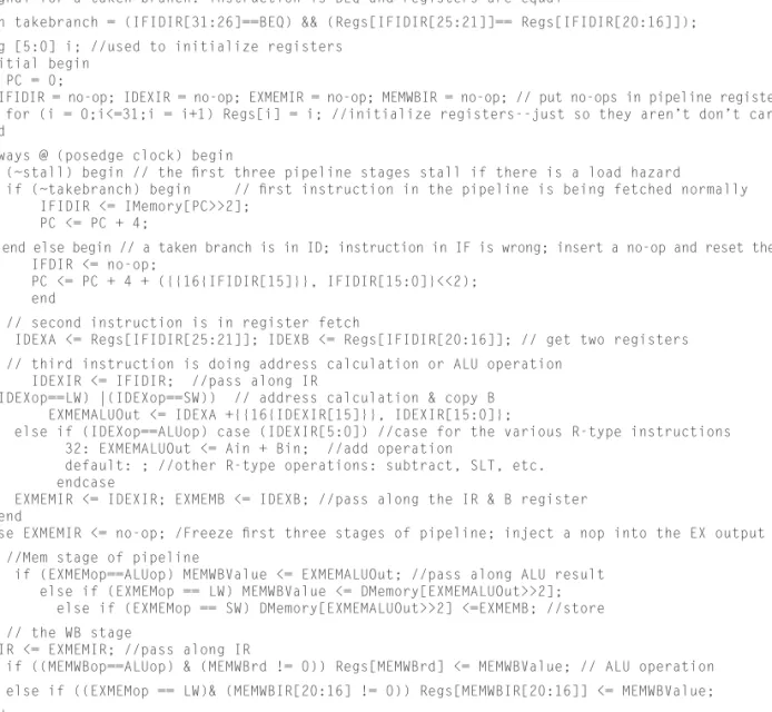
Figure 4.12.5 gives a behavioral specifi cation of a multicycle implementation
of the MIPS processor. Because of the use of behavioral operations, it would be
diffi cult to synthesize a sepa rate datapath and control unit with any reasonable
effi ciency. This version demonstrates another approach to the control by using a
Mealy fi nite-state machine (see discussion in Section C.10 of
Appendix C). The
use of a Mealy machine, which allows the output to depend both on inputs and the
current state, allows us to decrease the total number of states.
Since a version of the MIPS design intended for synthesis is considerably
more complex, we have relied on a number of Ver ilog modules that were specifi ed
in
Appendix C, including the following:
■
The 4-to-1 multiplexor shown in Figure C.4.2, and the 3-to-1 multiplexor
that can be trivially derived based on the 4-to-1 multiplexor.
■
The MIPS ALU shown in Figure C.5.15.
■
The MIPS ALU control defi ned in Figure C.5.16.
■
The MIPS register fi le defi ned in Figure C.8.11.
Now, let’s look at a Verilog version of the MIPS processor intended for synthesis.
Figure 4.12.6 shows the structural version of the MIPS datapath. Figure 4.12.7 uses
the datapath module to specify the MIPS CPU. This version also demonstrates
another approach to implementing the control unit, as well as some optimi zations
that rely on relationships between various control signals. Observe that the state
machine specifi cation only provides the sequencing actions.
The setting of the control lines is done with a series of
assign
statements that
depend on the state as well as the opcode fi eld of the instruction register. If one
were to fold the setting of the control into the state specifi cation, this would look
like a Mealy-style fi nite-state control unit. Because the setting of the control lines
is specifi ed using
assign
statements outside of the
always
block, most logic
synthesis systems will generate a small imple mentation of a fi nite-state machine
that determines the setting of the state register and then uses external logic to
derive the control inputs to the datapath.
In writing this version of the control, we have also taken advantage of a number
of insights about the relationship between various control signals as well as
situations where we don’t care about the control signal value; some examples of
these are given in the following elaboration.
module CPU (clock);
parameter LW = 6’b100011, SW = 6’b101011, BEQ=6’b000100, J=6’d2; input clock; //the clock is an external input
// The architecturally visible registers and scratch registers for implementation reg [31:0] PC, Regs[0:31], Memory [0:1023], IR, ALUOut, MDR, A, B;
reg [2:0] state; // processor state
wire [5:0] opcode; //use to get opcode easily
wire [31:0] SignExtend,PCOffset; //used to get sign-extended offset fi eld assign opcode = IR[31:26]; //opcode is upper 6 bits
assign SignExtend = {{16{IR[15]}},IR[15:0]}; //sign extension of lower 16 bits of instruction assign PCOffset = SignExtend << 2; //PC offset is shifted
// set the PC to 0 and start the control in state 0 initial begin PC = 0; state = 1; end
//The state machine--triggered on a rising clock always @(posedge clock) begin
Regs[0] = 0; //make R0 0 //shortcut way to make sure R0 is always 0 case (state) //action depends on the state
1: begin // fi rst step: fetch the instruction, increment PC, go to next state IR <= Memory[PC>>2];
PC <= PC + 4;
state = 2; //next state end
2: begin // second step: Instruction decode, register fetch, also compute branch address A <= Regs[IR[25:21]];
B <= Regs[IR[20:16]]; state = 3;
ALUOut <= PC + PCOffset; // compute PC-relative branch target end
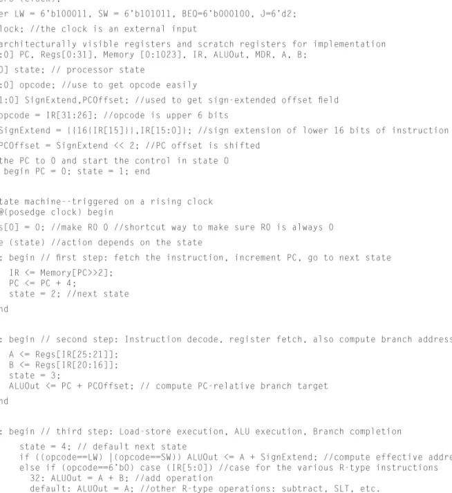
3: begin // third step: Load-store execution, ALU execution, Branch completion state = 4; // default next state
if ((opcode==LW) |(opcode==SW)) ALUOut <= A + SignExtend; //compute effective address else if (opcode==6’b0) case (IR[5:0]) //case for the various R-type instructions 32: ALUOut = A + B; //add operation
default: ALUOut = A; //other R-type operations: subtract, SLT, etc. endcase
FIGURE 4.12.5 A behavioral specifi cation of the multicycle MIPS design. This has the same cycle behavior as the multicycle design, but is purely for simulation and specifi cation. It cannot be used for synthesis. (con tinues on next page)
else if (opcode == BEQ) begin
if (A==B) PC <= ALUOut; // branch taken--update PC state = 1;
end
else if (opocde=J) begin
PC = {PC[31:28], IR[25:0],2’b00}; // the jump target PC state = 1;
end //Jumps
else ; // other opcodes or exception for undefi ned instruction would go here end
4: begin
if (opcode==6’b0) begin //ALU Operation
Regs[IR[15:11]] <= ALUOut; // write the result state = 1;
end //R-type fi nishes
else if (opcode == LW) begin // load instruction MDR <= Memory[ALUOut>>2]; // read the memory state = 5; // next state
end
else if (opcode == LW) begin
Memory[ALUOut>>2] <= B; // write the memory state = 1; // return to state 1
end //store fi nishes
else ; // other instructions go here end
5: begin // LW is the only instruction still in execution Regs[IR[20:16]] = MDR; // write the MDR to the register state = 1;
end //complete an LW instruction endcase
end endmodule
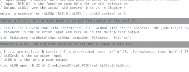
module Datapath (ALUOp, RegDst, MemtoReg, MemRead, MemWrite, IorD, RegWrite, IRWrite,
PCWrite, PCWriteCond, ALUSrcA, ALUSrcB, PCSource, opcode, clock); // the control inputs + clock input [1:0] ALUOp, ALUSrcB, PCSource; // 2-bit control signals
input RegDst, MemtoReg, MemRead, MemWrite, IorD, RegWrite, IRWrite, PCWrite, PCWriteCond, ALUSrcA, clock; // 1-bit control signals
output [5:0] opcode ;// opcode is needed as an output by control
reg [31:0] PC, Memory [0:1023], MDR,IR, ALUOut; // CPU state + some temporaries
wire [31:0] A,B,SignExtendOffset, PCOffset, ALUResultOut, PCValue, JumpAddr, Writedata, ALUAin, ALUBin,MemOut; / these are signals derived from registers
wire [3:0] ALUCtl; //. the ALU control lines wire Zero; the Zero out signal from the ALU
wire[4:0] Writereg;// the signal used to communicate the destination register initial PC = 0; //start the PC at 0
//Combinational signals used in the datapath
// Read using word address with either ALUOut or PC as the address source assign MemOut = MemRead ? Memory[(IorD ? ALUOut : PC)>>2]:0;
assign opcode = IR[31:26];// opcode shortcut
// Get the write register address from one of two fi elds depending on RegDst assign Writereg = RegDst ? IR[15:11]: IR[20:16];
// Get the write register data either from the ALUOut or from the MDR assign Writedata = MemtoReg ? MDR : ALUOut;
// Sign-extend the lower half of the IR from load/store/branch offsets
assign SignExtendOffset = {{16{IR[15]}},IR[15:0]}; //sign-extend lower 16 bits; // The branch offset is also shifted to make it a word offset
assign PCOffset = SignExtendOffset << 2;
// The A input to the ALU is either the rs register or the PC assign ALUAin = ALUSrcA ? A : PC; //ALU input is PC or A // Compose the Jump address
assign JumpAddr = {PC[31:28], IR[25:0],2’b00}; //The jump address
FIGURE 4.12.6 A Verilog version of the multicycle MIPS datapath that is appropriate for synthe sis. This datapath relies on several units from Appendix C. Initial statements do not synthesize, and a version used for synthesis would have to incorporate a reset signal that had this effect. Also note that resetting R0 to 0 on every clock is not the best way to ensure that R0 stays 0; instead, modifying the register fi le module to produce 0 whenever R0 is read and to ignore writes to R0 would be a more effi cient solution. (continues on next page)
// Creates an instance of the ALU control unit (see the module defi ned in Figure C.5.16 on page C-38 // Input ALUOp is control-unit set and used to describe the instruction class as in Chapter 4 // Input IR[5:0] is the function code fi eld for an ALU instruction
// Output ALUCtl are the actual ALU control bits as in Chapter 4 ALUControl alucontroller (ALUOp,IR[5:0],ALUCtl); //ALU control unit // Creates a 3-to-1 multiplexor used to select the source of the next PC
// Inputs are ALUResultOut (the incremented PC) , ALUOut (the branch address), the jump target address
// PCSource is the selector input and PCValue is the multiplexor output Mult3to1 PCdatasrc (ALUResultOut,ALUOut,JumpAddr, PCSource , PCValue); // Creates a 4-to-1 multiplexor used to select the B input of the ALU
// Inputs are register B,constant 4, sign-extended lower half of IR, sign-extended lower half of IR << 2 // ALUSrcB is the selector input
// ALUBin is the multiplexor output
Mult4to1 ALUBinput (B,32’d4,SignExtendOffset,PCOffset,ALUSrcB,ALUBin);
// Creates a MIPS ALU
// Inputs are ALUCtl (the ALU control), ALU value inputs (ALUAin, ALUBin) // Outputs are ALUResultOut (the 32-bit output) and Zero (zero detection output) MIPSALU ALU (ALUCtl, ALUAin, ALUBin, ALUResultOut,Zero); //the ALU
// Creates a MIPS register fi le // Inputs are
// the rs and rt fi elds of the IR used to specify which registers to read,
// Writereg (the write register number), Writedata (the data to be written), RegWrite (indicates a
write), the clock
// Outputs are A and B, the registers read
registerfi le regs (IR[25:21],IR[20:16],Writereg,Writedata,RegWrite,A,B,clock); //Register fi le // The clock-triggered actions of the datapath
always @(posedge clock) begin if (MemWrite) Memory[ALUOut>>2] <= B; // Write memory--must be a store ALUOut <= ALUResultOut; //Save the ALU result for use on a later clock cycle
if (IRWrite) IR <= MemOut; // Write the IR if an instruction fetch MDR <= MemOut; // Always save the memory read value
// The PC is written both conditionally (controlled by PCWrite) and unconditionally if (PCWrite || (PCWriteCond & Zero)) PC <=PCValue;
end endmodule
module CPU (clock);
parameter LW = 6’b100011, SW = 6’b101011, BEQ = 6’b000100, J = 6’d2; //constants input clock; reg [2:0] state;
wire [1:0] ALUOp, ALUSrcB, PCSource; wire [5:0] opcode;
wire RegDst, MemRead, MemWrite, IorD, RegWrite, IRWrite, PCWrite, PCWriteCond, ALUSrcA, MemoryOp, IRWwrite, Mem2Reg;
// Create an instance of the MIPS datapath, the inputs are the control signals; opcode is only output Datapath MIPSDP (ALUOp,RegDst,Mem2Reg, MemRead, MemWrite, IorD, RegWrite,
IRWrite, PCWrite, PCWriteCond, ALUSrcA, ALUSrcB, PCSource, opcode, clock); initial begin state = 1; end // start the state machine in state 1
// These are the defi nitions of the control signals assign IRWrite = (state==1);
assign Mem2Reg = ~ RegDst;
assign MemoryOp = (opcode==LW)|(opcode==SW); // a memory operation
assign ALUOp = ((state==1)|(state==2)|((state==3)&MemoryOp)) ? 2’b00 : // add ((state==3)&(opcode==BEQ)) ? 2’b01 : 2’b10; // subtract or use function code assign RegDst = ((state==4)&(opcode==0)) ? 1 : 0;
assign MemRead = (state==1) | ((state==4)&(opcode==LW)); assign MemWrite = (state==4)&(opcode==SW);
assign IorD = (state==1) ? 0 : (state==4) ? 1 : X; assign RegWrite = (state==5) | ((state==4) &(opcode==0)); assign PCWrite = (state==1) | ((state==3)&(opcode==J)); assign PCWriteCond = (state==3)&(opcode==BEQ);
assign ALUSrcA = ((state==1)|(state==2)) ? 0 :1;
assign ALUSrcB = ((state==1) | ((state==3)&(opcode==BEQ))) ? 2’b01 : (state==2) ? 2’b11 : ((state==3)&MemoryOp) ? 2’b10 : 2’b00; // memory operation or other
assign PCSource = (state==1) ? 2’b00 : ((opcode==BEQ) ? 2’b01 : 2’b10); // Here is the state machine, which only has to sequence states
always @(posedge clock) begin // all state updates on a positive clock edge case (state)
1: state = 2; //unconditional next state 2: state = 3; //unconditional next state 3: // third step: jumps and branches complete
state = ((opcode==BEQ) | (opcode==J)) ? 1 : 4;// branch or jump go back else next state 4: state = (opcode==LW) ? 5 : 1; //R-type and SW fi nish
5: state = 1; // go back endcase
end
endmodule
Elaboration:
When specifying control, designers often take advantage of knowledge
of the control so as to simplify or shorten the control specifi ca tion. Here are a few
exam-ples from the specifi cation in Figures 4.12.6 and 4.12.7.
1.
MemtoRegis set only in two cases, and then it is always the inverse of
RegDst, so
we just use the inverse of
RegDst.
2.
IRWriteis set only in state 1.
3. The ALU does not operate in every state and, when unused, can safely do
any-thing.
4.
RegDstis 1 in only one case and can otherwise be set to 0. In practice it might be
better to set it explicitly when needed and otherwise set it to X, as we do for
IorD.
First, it allows additional logic optimization possibilities through the exploitation of
don’t-care terms (see
Ap pendix C
for further discussion and examples). Second,
it is a more pre cise specifi cation, and this allows the simulation to more closely
model the hardware, possibly uncovering additional errors in the specifi ca tion.
More Illustrations of Instruction Execution on the
Hardware
To reduce the cost of this book, in the third edition we moved sections and fi gures
that were used by a minority of instructors onto a companion CD. This subsection
recaptures those fi gures for readers who would like more supplemental material to
better understand pipelining. These are all single-clock-cycle pipeline diagrams,
which take many fi gures to illustrate the execution of a sequence of instructions.
The three examples are for code with no hazards, an example of forwarding
on the pipelined implementation, and an example of bypassing on the pipelined
implementation.
No Hazard Illustrations
On page 356, we gave the example code sequence
lw $10, 20($1)
sub $11, $2, $3
Figures 4.43 and 4.44 showed the multiple-clock-cycle pipeline diagrams for this
two-instruction sequence exe cuting across six clock cycles. Figures 4.12.8 through
4.12.10 show the corresponding single-clock-cycle pipeline diagrams for these
two instructions. Note that the order of the instructions differs between these two
types of diagrams: the newest instruction is at the
bottom and to the right
of the
multiple-clock-cycle pipeline diagram, and it is on the
left
in the single-clock-cycle
pipeline diagram.
FIGURE 4.12.8 Single-cycle pipeline diagrams for clock cycles 1 (top diagram) and 2 (bottom diagram). This style of pipeline representation is a snap shot of every instruction executing during one clock cycle. Our example has but two instructions, so at most two stages are identifi ed in each clock cycle; normally, all fi ve stages are occupied. The highlighted portions of the datapath are active in that clock cycle. The load is fetched in clock cycle 1 and decoded in clock cycle 2, with the subtract fetched in the second clock cycle. To make the fi gures easier to understand, the other pipeline stages are empty, but normally there is an instruction in every pipeline stage.
Instruction memory Address 4 32 Instruction
IF/ID EX/MEM MEM/WB
Add Add PC Registers Read data 1 Read data 2 Read register 1 Read register 2 16 Sign- extend Write register Write data ID/EX Instruction decode lw $10,20($1) Instruction fetch sub $11,$2,$3 Instruction memory Address 4 32 Add Add result Shift left 2 Shift left 2 Instruction IF/ID EX/MEM PC Write data Registers Read data 1 Read data 2 Read register 1 Read register 2 16 Write register Write data Read data ALU result ALU Zero Add Add result ALU result ALU Zero ID/EX Instruction fetch lw $10,20($1) Address Data memory Write data Read data Address Data memory Clock 1 Clock 2 M u x 0 1 M u x 0 1 M u x 0 1 M u x 1 0 M u x 1 0 M u x 0 1 Sign- extend MEM/WB
FIGURE 4.12.9 Single-cycle pipeline diagrams for clock cycles 3 (top diagram) and 4 (bottom diagram). In the third clock cycle in the top diagram, lw enters the EX stage. At the same time, sub enters ID. In the fourth clock cycle (bottom datapath), lw moves into MEM stage,
Instruction memory Address 4 32 Instruction
IF/ID EX/MEM MEM/WB
Add Add Registers Read data 1 Read data 2 Read register 1 Read register 2 16 Sign-extend Sign-extend Write register Write data ID/EX Memory lw $10,20($1) Execution sub $11,$2,$3 Instruction memory Address 4 32 Add Add result Shift left 2
AddresultAdd Shift
left 2
Instruction
IF/ID EX/MEM MEM/WB
PC PC Write data Registers Read data 1 Read data 2 Read register 1 Read register 2 16 Write register Write data Read data ALU result ALU Zero ALU result ALU Zero ID/EX Address Data memory Write data Read data Address Data memory Clock 3 Clock 4 M u x 0 1 M u x 0 1 M u x 0 1 M u x 1 0 M u x 1 0 M u x 0 1 Instruction decode sub $11,$2,$3 Execution lw $10,20($1)
FIGURE 4.12.10 Single-cycle pipeline diagrams for clock cycles 5 (top diagram) and 6 (bottom diagram). In clock cycle 5, lw completes by writing the data in MEM/WB into register 10, and sub sends the difference in EX/MEM to MEM/WB. In the next clock cycle, sub writes the value in MEM/WB to register 11.
PC Instruction memory Registers Control M u x M u x M u x Data memory M u ALU x Instruction IF/IDWrite ID/EX.MemRead PCWrite ID/EX EX/MEM MEM/WB 1 1 X X 1 X 2 ID/EX.RegisterRt $X $1 0 11 EX WB WB M Forwarding unit Hazard detection unit M u x IF/ID
More Examples
To understand how pipeline control works, let’s consider these fi ve instructions
going through the pipeline:
lw $10, 20($1)
sub $11, $2, $3
and $12, $4, $5
or $13, $6, $7
add $14, $8, $9
Figures 4.12.11 through 4.12.15 show these instructions pro
ceeding through the
nine clock cycles it takes them to complete exe cution, highlighting what is active in a
FIGURE 4.12.11 Clock cycles 1 and 2. The phrase “before<i>” means the ith instruction before lw. The lw instruction in the top datapath is in the IF stage. At the end of the clock cycle, the lw instruction is in the IF/ID pipeline registers. In the second clock cycle, seen in the bottom datapath, the lw moves to the ID stage, and sub enters in the IF stage. Note that the values of the instruction fi elds and the selected source registers are shown in the ID stage. Hence register $1 and the constant 20, the operands of lw, are written into the ID/EX pipeline register. The number 10, representing the destination reg ister number of lw, is also placed in ID/EX. Bits 15–11 are 0, but we use X to show that a fi eld plays no role in a given instruction. The top of the ID/EX pipeline register shows the control values for lw to be used in the remaining stages. These control values can be read from the lw row
Instruction [20–16] MemtoReg ALUOp Branch RegDst ALUSrc 4 Instruction [15–0] ALU control RegWrite MemRead Control Instruction [15–11] EX M WB M WB WB Instruction
IF/ID ID/EX EX/MEM
ID: before<1> EX: before<2> MEM: before<3> WB: before<4> MEM/WB IF: lw $10,20($1) 000 00 0000 000 00 00 0 0 00 0 0 0 0 0 1 PC WB EX M MemtoReg ALUOp Branch RegDst ALUSrc 4 ALU control RegWrite M WB WB Instruction IF/ID ID: lw $10,20($1) EX: before<1> MEM: before<2> WB: before<3> MEM/WB IF: sub $11,$2,$3 010 11 0001 000 00 00 0 0 00 0 0 0 0 0 PC lw Control X 1 Instruction [20–16] Instruction [15–0] Instruction [15–11] 20 $X $1 10 X MemWrite MemRead MemWrite Clock 2 Clock 1 M u x 0 1 M u x 0 1 M u x 1 0 M u x 0 1 M u x 0 1 M u x 0 1 M u x 0 1 M u x 0 Add Add Instruction memory Address Instruction memory Address Registers Read data 1 Read data 2 Read register 1 Read register 2 Write register Registers Read data 1 Read data 2 Read register 1 Read register 2 Write register Write data Write data Write data Read data ALU result ALU Zero Address Data memory Write data Read data Address Data memory Sign-extend Sign-extend X 10 20 EX/MEM ID/EX ALU result ALU Zero Shift left 2 Add Add result Shift left 2 Add Add result
Instruction [20–16] MemtoReg ALUOp Branch RegDst ALUSrc 4 Instruction [15–0] Shift left 2 RegWrite MemRead Control Instruction [15–11] EX M WB M WB WB Instruction
IF/ID ID/EX EX/MEM
ID: sub $11,$2,$3 EX: lw $10,... MEM: before<1> WB: before<2> MEM/WB IF: and $12,$4,$5 000 10 1100 010 11 00 0 1 00 0 0 0 0 0 1 PC WB EX M MemtoReg ALUOp Branch RegDst ALUSrc 4 ALU control ALU control Shift left 2 RegWrite WB WB Instruction IF/ID
ID: and $12,$4,$5 EX: sub $11,... MEM: lw $10,... WB: before<1>
MEM/WB IF: or $13,$6,$7 000 10 1100 000 10 10 1 0 11 1 0 0 0 0 PC and Control 5 4 Instruction [20–16] Instruction [15–0] Instruction [15–11] X $5 $4 $3 $2 X 20 10 12 10 11 MemWrite MemRead MemWrite Clock 4 Clock 3 M u x 0 1 M u x 0 1 M u x 1 0 M u x 0 1 M u x 0 1 M u x 0 1 M u x 0 1 M u x 0 Add Add Instruction memory Address Instruction memory Address Registers Read data 1 Read data 2 Read register 1 Read register 2 Write register Registers Read data 1 Read data 2 Read register 1 Read register 2 Write register Write data Write data
AddresultAdd
Write data Read data ALU result ALU Zero
AddresultAdd
Address Data memory Write data Read data Address Data memory Sign-extend Sign-extend 12 X X EX/MEM ID/EX ALU result ALU Zero 2 3 $2 $1 $3 X X 11 X X 11 M
FIGURE 4.12.12 Clock cycles 3 and 4. In the top diagram,lw enters the EX stage in the third clock cycle, adding $1 and 20 to form the address in the EX/MEM pipeline register. (The lw instruction is written lw $10,... upon reaching EX, because the identity of instruction operands is not needed by EX or the subse quent stages. In this version of the pipeline, the actions of EX, MEM, and WB depend only on the instruction and its destination register or its target address.) At the same time, sub enters ID, reading registers $2 and $3, and the and instruction starts IF. In the fourth clock cycle (bottom datapath), lw moves into MEM stage, reading memory using the value in EX/MEM as the address. In the same clock cycle, the ALU subtracts $3 from $2 and places the difference into EX/MEM registers $4 and $5 are read during ID and the or instruc tion enters IF. The two diagrams show the control signals being created in the ID stage and peeled off as they are used in subsequent pipe stages.
Instruction [20–16] MemtoReg ALUOp Branch RegDst ALUSrc 4 Instruction [15–0] Shift left 2 RegWrite MemRead Control Instruction [15–11] EX M WB M WB WB Instruction IF/ID or EX/MEM ID/EX ID: or $13,$6,$7 EX: and $12,... MEM: sub $11,... WB: lw $10,.. MEM/WB IF: add $14,$8,$9 000 10 1100 000 10 10 1 0 10 0 0 0 1 1 1 PC WB EX M MemtoReg ALUOp Branch RegDst ALUSrc 4 ALU control ALU control Shift left 2 RegWrite M WB WB Instruction IF/ID ID: add $14,$8,$9 EX: or $13,... MEM: and $12,... WB: sub $11,. MEM/WB IF: after<1> 000 10 1100 000 10 10 1 0 10 0 0 0 1 0 PC add Control 9 11 8 Instruction [20–16] Instruction [15–0] Instruction [15–11] X $9 $8 $7 $6 X 11 10 14 12 11 13 MemWrite MemRead MemWrite Clock 6 Clock 5 M u x 0 1 M u x 0 1 M u x 1 0 M u x 0 1 M u x 0 1 M u x 0 1 M u x 0 1 M u x 0 Add Add Instruction memory Address Instruction memory Address Registers Read data 1 Read data 2 Read register 1 Read register 2 Write register Registers Read data 1 Read data 2 Read register 1 Read register 2 Write register Write data Write data AddAdd result Write data Read data ALU result ALU Zero Add Add result Address Data memory Write data Read data Address Data memory Sign-extend Sign-extend 12 X X EX/MEM ID/EX ALU result ALU Zero 6 7 10 $6 $4 $5 $7 X X 13 X X 13 12
FIGURE 4.12.13 Clock cycles 5 and 6. With add, the fi nal instruction in this example, entering IF in the top datapath, all instructions are engaged. By writing the data in MEM/WB into register 10, lw com pletes; both the data and the register number are in MEM/WB. In the same clock cycle, sub sends the differ ence in EX/MEM to MEM/WB, and the rest of the instructions move forward. In the next clock cycle, sub selects the value in MEM/WB to write to register number 11, again found in MEM/WB. The remaining instructions play follow-the-leader: the ALU calculates the OR of
Instruction [20–16] MemtoReg ALUOp Branch RegDst ALUSrc 4 Instruction [15–0] ALU control Shift left 2 RegWrite MemRead Control Instruction [15–11] EX M WB M WB WB Instruction
IF/ID ID/EX EX/MEM
ID: after<1> EX: add $14,... MEM: or $13,... WB: and $12,. MEM/WB IF: after<2> 000 00 0000 000 10 10 1 0 10 0 0 0 1 0 1 PC WB EX M MemtoReg ALUOp Branch RegDst ALUSrc 4 ALU control Shift left 2 RegWrite M WB WB Instruction IF/ID ID: after<2> EX: after<1> MEM: add $14,... WB: or $13,.. MEM/WB IF: after<3> 000 00 0000 000 00 00 0 0 10 0 0 0 1 0 PC Control 13 Instruction [20–16] Instruction [15–0] Instruction [15–11] 14 13 MemWrite MemRead MemWrite Clock 8 Clock 7 M u x 0 1 M u x 0 1 M u x 1 0 M u x 0 1 M u x 0 1 M u x 0 1 M u x 0 1 M u x 0 Add Add Instruction memory Address Instruction memory Address Registers Read data 1 Read data 2 Read register 1 Read register 2 Write register Registers Read data 1 Read data 2 Read register 1 Read register 2 Write register Write data Add Add result Write data Read data ALU result ALU Zero
AddresultAdd
Address Data memory Write data Read data Address Data memory Sign-extend Sign-extend EX/MEM ID/EX ALU result ALU Zero 12 $8 $9 14 13 12 Write data
FIGURE 4.12.14 Clock cycles 7 and 8. In the top datapath, the add instruction brings up the rear, adding the values corresponding to registers $8 and $9 during the EX stage. The result of the or instruction is passed from EX/MEM to MEM/WB in the MEM stage, and the WB stage writes the result of the and instruction in MEM/WB to register $12. Note that the control signals are deasserted (set to 0) in the ID stage, since no instruction is being executed. In the following clock cycle (lower drawing), the WB stage writes the result to register $13, thereby completing or, and the MEM stage passes the sum from the add in EX/MEM to MEM/WB. The instructions after add are shown as inac tive for pedagogical reasons.
FIGURE 4.12.15 Clock cycle 9. The WB stage writes the sum in MEM/WB into reg ister $14, completing add and the fi ve-instruction sequence. The instructions after add are shown as inactive for pedagogical reasons.
WB EX M MemtoReg ALUOp Branch RegDst ALUSrc 4 ALU control Shift left 2 RegWr ite M WB WB Instr uction IF/ID ID: after<3> EX: after<2> MEM: after<1> WB: add $14,. MEM/WB IF: after<4> 000 00 0000 000 00 00 0 0 00 0 0 0 1 0 PC Control 14 Instruction [20–16] Instruction [15–0] Instruction [15–11] 14 MemRead MemWr ite Clock 9 M u x 0 1 M u x 0 1 M u x 1 0 M u x 0 1 Add Instruction memory Address Registers Read data 1 Read data 2 Read register 1 Read register 2 Write register Write data Add Add result Write data Read data Address Data memory Sign-extend EX/MEM ID/EX ALU result ALU Zero
stage and identifying the instruction associated with each stage during a clock cycle. If
you examine them carefully, you may notice:
■
In Figure 4.12.13 you can see the sequence of the destination register numbers
from left to right at the bottom of the pipeline registers. The numbers advance to
the right during each clock cycle, with the MEM/WB pipeline register sup plying
the number of the register written during the WB stage.
■
When a stage is inactive, the values of control lines that are deasserted are shown
as 0 or X (for don’t care).
■
Sequencing of control is embedded in the pipeline structure itself. First, all
instructions take the same number of clock cycles, so there is no special control
for instruction dura tion. Second, all control information is computed during
instruction decode and then passed along by the pipeline registers.
Forwarding Illustrations
We can use the single-clock-cycle pipeline diagrams to show how forwarding
operates, as well as how the control activates the forwarding paths. Consider the
following code sequence in which the dependences have been highlighted:
sub
$2
, $1, $3
and
$4
,
$2
, $5
or
$4
,
$4
,
$2
add $9,
$4
,
$2
Figures 4.12.16 and 4.12.17 show the events in clock cycles 3–6 in the execution of
these instructions.
In clock cycle 4, the forwarding unit sees the writing by the
sub
instruction of
register
$2
in the MEM stage, while the
and
instruction in the EX stage is reading
register
$2
. The forwarding unit selects the EX/MEM pipeline register instead of
the ID/EX pipeline register as the upper input to the ALU to get the proper value
for register
$2
. The following
or
instruction reads register
$4
, which is written by
the
and
instruction, and register
$2
, which is written by the
sub
instruction.
Thus, in clock cycle 5, the forwarding unit selects the EX/MEM pipeline register
for the upper input to the ALU and the MEM/WB pipeline register for the lower
input to the ALU. The following
add
instruction reads both register
$4
, the target
of the
and
instruc tion, and register
$2
, which the
sub
instruction has already
writ-ten. Notice that the prior two instructions both write register
$4
, so the forwarding
unit must pick the immediately preceding one (MEM stage).
In clock cycle 6, the forwarding unit thus selects the EX/MEM pipeline register,
containing the result of the
or
instruction, for the upper ALU input but uses the
nonforwarding register value for the lower input to the ALU.
Illustrating Pipelines with Stalls and Forwarding
We can use the single-clock-cycle pipeline diagrams to show how the control
for stalls works. Figures 4.12.18 through 4.12.20 show the single-cycle diagram for
clocks 2 through 7 for the following code sequence (dependences highlighted):
lw
$2
, 20($1)
and $4,
$2
,$5
or $4,
$4
,
$2
FIGURE 4.12.16 Clock cycles 3 and 4 of the instruction sequence on page 4.12-25. The bold lines are those active in a clock cycle, and the italicized register numbers in color indicate a hazard. The forwarding unit is highlighted by shading it when it is forwarding data to the ALU. The
PC Instruction memory Registers M u x M u x M u x EX M WB WB Data memory M u x Forwarding unit Instr uction IF/ID and $4,$2,$5 sub $2, $1, $3 ID/EX before<1> EX/MEM before<2> MEM/WB or $4,$4,$2 Clock 3 2 5 10 10 $2 $5 5 2 4 $1 $3 3 1 2 Control ALU M WB PC Instruction memory Registers M u x M u x M u x EX M WB Data memory M u x Forwarding unit Instr uction IF/ID or $4,$4,$2 and $4,$2,$5 ID/EX sub $2,... EX/MEM before<1> MEM/WB add $9,$4,$2 Clock 4 4 2 10 10 10 $4 $2 2 4 4 $2 $5 5 2 2 4 Control ALU M WB WB
FIGURE 4.12.17 Clock cycles 5 and 6 of the instruction sequence on page 4.12-25. The forwarding unit is highlighted when it is forwarding data to the ALU. The two instructions after add are shown as inactive just to emphasize what occurs for the four instructions in the example. The bold lines are those active in a clock cycle, and the italicized register numbers in color indicate a hazard.
PC Instruction memory Registers Control M u x Data memory M u x M u x M u x ALU Instr uction IF/ID add $9,$4,$2 or $4,$4,$2 ID/EX and $4,... EX/MEM sub $2,.. MEM/WB after<1> Clock 5 4 2 2 4 2 4 2 9 4 $2 $4 $2 $4 10 10 10 1 4 2 after<1> after<2> add $9,$4,$2 or $4,... EX/MEM and $4,.. MEM/WB ID/EX EX WB M WB WB M Forwarding unit PC Instruction memory Registers Control M u x M u x M u x Data memory M u ALU x Instr uction IF/ID Clock 6 4 4 2 9 $2 $4 10 10 1 4 4 EX WB M WB WB M Forwarding unit
FIGURE 4.12.18 Clock cycles 2 and 3 of the instruction sequence on page 4.12-25 with a load replacing sub. The bold lines are those active in a clock cycle, the italicized register numbers in color indicate a hazard, and the . . . in the place of operands means that their identity is information not needed by that stage. The values of the signifi cant control lines, registers, and register numbers are labeled in the fi gures. The and instruction wants to read the value created by the lw instruction in clock cycle 3, so the hazard detection unit stalls the and and or instructions. Hence,
Registers Instr uction ID/EX 2 5 Control PC Instruction memory PC Instructionmemory Hazard detection unit 0 M u x IF/ID Wr ite PCWr ite IF/ID Wr ite PCWr ite ID/EX.RegisterRt before<3> Registers M u x M u x EX M WB M WB Data memory M u x Instr uction IF/ID lw $2,20($1) ID/EX before<2> EX/MEM MEM/WB Clock 2 1 1 X X 11 $1 $X X 2 1 Control ALU WB lw $2,20($1) before<1> before<2> or $4,$4,$2 and $4,$2,$5 and $4,$2,$5 Clock 3 M u x M u x M u x EX M WB M WB Data memory M u x Forwarding unit Forwarding unit EX/MEM MEM/WB 00 11 $1 $X X 1 2 $5 $2 2 5 5 4 2 ALU WB Hazard detection unit 0 M u x ID/EX.RegisterRt before<1> ID/EX.MemRead ID/EX.MemRead M u x IF/ID
FIGURE 4.12.19 Clock cycles 4 and 5 of the instruction sequence on page 4.12-25 with a load replacing sub. The bubble is inserted in the pipeline in clock cycle 4, and then the and instruction is allowed to proceed in clock cycle 5. The forwarding unit is highlighted in clock cycle 5 because it is for warding data from lw to the ALU. Note that in clock cycle 4, the forwarding unit forwards the address of the lw as if it were the contents of register $2; this is rendered harmless by the insertion of the bubble. The bold lines are those active in a clock cycle, and the italicized register numbers in color indicate a hazard.
Registers Instruction ID/EX 4 2 2 Control PC Instruction memory PC Instructionmemory Hazard detection unit 0 M u x IF/IDWrite PCWrite IF/IDWrite PCWrite ID/EX.RegisterRt before<1> Registers M u x M u x EX M WB M WB Data memory M u x Instruction IF/ID and $4,$2,$5 ID/EX lw $2,... EX/MEM MEM/WB Clock 4 2 2 5 5 10 00 11 $2 $5 5 4 2 $2 $5 5 4 2 2 Control ALU WB and $4,$2,$5 Bubble lw $2,... add $9,$4,$2 or $4,$4,$2 or $4,$4,$2 Clock 5 M u x M u x M u x EX M WB M WB Data memory M u x Forwarding unit Forwarding unit EX/MEM MEM/WB 10 10 11 2 0 $2 $5 5 4 4 $2 $4 2 5 2 4 2 ALU WB Hazard detection unit 0 M u x ID/EX.RegisterRt Bubble ID/EX.MemRead ID/EX.MemRead M u x IF/ID
Registers Instr uction ID/EX 4 Control PC Instruction memory PC Instructionmemory Hazard detection unit 0 M u x IF/ID Wr ite PCWr ite IF/ID Wr ite PCWr ite ID/EX.RegisterRt Bubble Registers M u x M u x EX M WB M WB Data memory M u x Instr uction IF/ID add $9,$4,$2 ID/EX and $4,... EX/MEM MEM/WB Clock 6 4 4 2 2 10 10 10 0 $4 $2 2 9 4 $4 $2 2 4 4 4 Control ALU WB add $9,$4,$2 or $4,... and $4,... after<2> after<1> after<1> Clock 7 M u x M u x M u x EX M WB M WB Data memory M u x Forwarding unit Forwarding unit EX/MEM MEM/WB 10 10 1 4 4 10 $4 $2 2 9 4 ALU WB Hazard detection unit 0 M u x ID/EX.RegisterRt or $4,$4,$2 ID/EX.MemRead ID/EX.MemRead M u x IF/ID
FIGURE 4.12.20 Clock cycles 6 and 7 of the instruction sequence on page 4.12-25 with a load replacing sub. Note that unlike in Figure 4.12.17, the stall allows the lw to complete, and so there is no forwarding from MEM/WB in clock cycle 6. Register $4 for the add in the EX stage still depends on the result from or in EX/MEM, so the forwarding unit passes the result to the ALU. The bold lines show ALU input lines active in a clock cycle, and the italicized register numbers indicate a hazard. The instruc tions after add are shown as inactive for pedagogical reasons.