Available online: https://edupediapublications.org/journals/index.php/IJR/ P a g e | 2849
Graph-Based Transistor Network Generation Method for
Super gate Design
A. Venkatreddy & M.S. Shyam
M.Tech (VLSI&ES), St. Mary’s College of Engineering and Technology, Hyderabad Assistant Professor, St. Mary’s College of Engineering and Technology, Hyderabad
Abstract- Transistor organize improvement speaks to a compelling method for enhancing VLSI circuits. This paper proposes a novel technique to naturally create systems with negligible transistor check, beginning from an irredundant entirety of-items articulation as the info. The technique can convey both series– parallel (SP) and non-SP switch game plans, enhancing speed, control scattering, and range of CMOS entryways. Exploratory outcomes exhibit expected picks up in examination with related methodologies.
I. INTRODUCTION
In VLSI advanced outline, the flag postpone engendering, control dissemination, and zone of circuits are emphatically identified with the quantity of transistors (switches) [1]– [3]. Consequently, transistor course of action improvement is of exceptional intrigue when planning standard cell libraries and custom entryways [4], [5]. Switch based advancements, for example, CMOS, FinFET [6], and carbon nanotubes [7], can exploit such a change. In this way, efficient calculations to naturally produce advanced transistor systems are very helpful for planning computerized incorporated circuits (ICs). A few techniques have been exhibited in the writing for generating and optimizing transistor networks. Most customary arrangements depend on figuring Boolean articulations, in which just series– parallel (SP) relationship of transistors can be acquired from calculated structures. Then again, chart based strategies can find SP and furthermore non-SP (NSP) game plans with potential lessening in transistor check. In spite of the endeavors of past works, there is as yet a space for enhancing the age of transistor systems.
Fig.1: Transistor systems comparing. (a) SP arrangement from considered frame. (b)
Available online: https://edupediapublications.org/journals/index.php/IJR/ P a g e | 2850
execution methods of the proposed technique considering the limitation of gadgets in arrangement. Segment V exhibits the efficiency of the proposed approach by giving exploratory outcomes in regards to transistor tally, region estimation, entryway execution, and power dispersal.
Fig.2: CMOS segments
II. PROPOSED WORK
For assessment and approval, the proposed strategy was connected over various arrangements of delegate works so as to furnish a reasonable correlation with other accessible arrangements. Four diverse arrangements of capacities were considered: 1) the arrangement of 4-input P-class of capacities; 2) an arrangement of handmade systems that don't present transistors in SP affiliations.3) a given function with 11variablesas a more unpredictable contextual investigation; and 4) the capacities and transistor systems portrayed in the Ninomiya's index.
A. Transistor Count Evaluation the first analyze was completed over Boolean capacities up to four factors, speaking to 65536 capacities. These capacities were assembled into an arrangement of equal classes by considering input stage called, thus, 4-input P-class. This set contains 3982 agent capacities. The relating CMOS entryway for each capacity of this set was worked, by producing both the draw up and pull-down systems through the techniques in assessment. Table I demonstrates the outcomes got considering the aggregate transistor check used to construct all doors, including required information inverters. Notice that, lone info inverters are permitted. The second analysis
was done over an arrangement of 53 capacities acquired from high quality systems where there is neither arrangement nor parallel affiliations [8]. These systems have at most four transistors in arrangement, being reasonable for CMOS entryway execution. It speaks to a commendable benchmark set taken as reference to assess the proposed approach and other related strategies.
The vertical hub relates the quantity of capacities for each expansion on transistor check. As can be seen, our unbounded strategy could lessen up to eight transistors now and again. When all is said in done, the increases are around a few transistors for each system. Despite the fact that there is an expanding in transistor tally, the proposed strategy (limited) is close to the ideal transistor tally.
For this situation, the proposed strategy gives the transistors arrange displayed. This is the ideal arrangement with just 11 transistors. At long last, we have assessed the proposed technique utilizing the arrangement of 402 capacities/systems displayed in the Ninomiya's inventory, additionally received as benchmarking in different works. Kagaris and Haniotakis and Tanaka and Kambayashi assert that their strategies have gotten systems with an indistinguishable number of transistors from introduced in this index, aside from work N58 where they accomplished a decrease of one transistor. Our strategy isn't able to accomplish the best answer for all capacities gave in the inventory.
Available online: https://edupediapublications.org/journals/index.php/IJR/ P a g e | 2851
transistors in a system. Considering two systems with a similar transistor stack, the system containing fewer transistors normally has a superior execution. In this sense, execution upgrades can be seen in the similar examination. When contrasting the limited and the FC-MDC strategies, just the situations where the proposed technique diminished transistor tally were considered. Abatement in gadget tally tends to show a significant decrease in door control scattering. Fewer transistors in the entryway speak to less capacitance to be charged amid the signs exchanging. Only the situations where the proposed method reduced the number of transistors is considered. The outcomes confirmed that decreasing transistor tally prompts a power dispersal lessening. A power-defer investigation was performed contrasting limited and unbounded execution modes. This examination relates to the dynamic power part. The short out segment was not considered, since it for the most part speaks to <10% of the aggregate power scattering in all around planned circuits. As far as physical territory assessment, it is instinctive to expect region sparing when the quantity of gadgets is decreased. One could think in building painstakingly the format of an arrangement of systems. Be that as it may, such an undertaking is illogical and may come about even in an uncertain examination because of numerous different elements included.
The system format measurements can be assessed considering the typical standard cell layout, where pMOS transistors of the draw up organize are set over nMOS transistors of the draw down plane. Such a transistor situation is made side-by side, in line, investigating format methods like Euler ways. The Euler way examination gives a smart thought of design length, while the format tallness can be assessed considering the electrical cables, the P and N dynamic ranges, and the signs wire stuffing. Notice that the design compaction is a hard and carefully assembled tedious assignment not investigated in this paper. The Euler way (and possible dynamic zone breaks) and the flag steering were separated for each
produced organize. A region estimative assessment, considering just cases that the proposed strategy decreased transistor include, is demonstrated Fig. 28. Such cases include 1680 doors. For 254 doors, a territory increment was seen because of breaks addition keeping in mind the end goal to coordinate Euler ways. For 1186 entryways, a zone decrease was observed, demonstrating the propensity of the circuit zone sparing because of transistor tally diminishment.
Fig.3: Transistor networks corresponding to (1). (a) SP solution from factored form. (b) NSP from existing graph-based generation
methods. (c) Optimum NSP solution.
Fig.4: Representation of (a) switch element (ideal MOS transistor), where
x controls the connection between T and T1 terminals, and associations.
(b) Series. (c) Parallel. (d) SP. (e) NSP.
III. SWITCH NETWORK SYNTHESIS METHOD
Available online: https://edupediapublications.org/journals/index.php/IJR/ P a g e | 2852
Fig.5: Execution flow of the proposed method
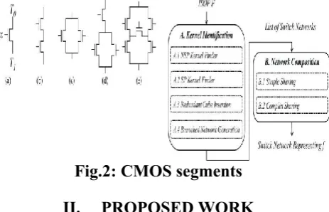
A. Kernel Identification
During the kernel identification module, an intermediate data structure called kernel is used to search for possible SP and NSP networks. A kernel of an ISOP F with m cubes is an undirected graph G = (V, E), where vertices in V = {v1, v2, . . ., vm} represent distinct cubes of F. An edge e = (vi , v j ) ∈ E, i _= j , exists if and only if vi ∩ v j _= ∅. Such edge e is labeled vi ∩ v j . Using the kernel structure, its possible to determine the relationship among cubes of F in order to perform logic sharing. This way, each step of the kernel identification module aims to extract kernels from F that leads to optimized switch count. The kernel identification module is divided in four steps, as presented in Fig. 3 (left) and in Algorithm 1. Each step is responsible for finding switch networks representing sub functions of the target function f. The NSP kernel finder step aims to obtain optimized NSP networks from an input ISOP F. When a switch network is found, the cubes used to achieve such network are removed from F. Such removal may lead to a simpler ISOP F1.
The SP kernel finder step, in turn, searches for SP networks using as the input F1. Similarly to the first step, the cubes of the found SP networks are removed from F1, resulting F2. Since the remaining cubes of F2 were not useful to produce NSP or SP networks, redundant cubes are added into the kernels in order to find NSP arrangements with redundant paths. Therefore, the cubes leading
to NSP networks with redundant paths are removed from F2, resulting F3.
Fig.6: (a) NSP kernel template. (b) Resulting switch network.
Fig.7: (a) NSP kernel K1, derived from (3). (b) Resulting switch network S1. Finally, a list of switch networks is produced as output of the kernel identification module. Each step of this first module is detailed presented below.
1) Non series–Parallel Kernel Finder: Let f be a Boolean function given in ISOP form F = c1 + · · · + cm, where m denotes the number of cubes in F. In order to identify kernels, the combinations of m cubes are taken four at a time, i.e., four-combination of cubes. The sum of such four cubes results in an ISOP H, which represents h that is a sub function of f. A kernel with four vertices is obtained from H. To ensure that the generated kernel results in a NSP switch network, two rules must be checked.
Rule 1: Let Ev be the set of edges connected to the
Available online: https://edupediapublications.org/journals/index.php/IJR/ P a g e | 2853
the edge e2 is moved to the place of e4, e4 is moved to the place of e3, and e3 is moved to the place of e2. By applying such a reordering, it is possible to achieve the network. The reordering procedure is necessary to ensure that each path of the switch network represents a cube from the sub function h.
The pseudo code of the NSP kernel finder step is presented in Algorithm 2. Let C be the set of all possible four combinations of cubes, generated by get Cube Combinations (line 2) procedure. Considering an ISOP F with m cubes, the get Cube Combinations has a time complexity of O(m4). Then, for each possible combination of four cubes, a kernel is obtained (line 5). The time complexity of the obtain kernel subroutine is O(m2n), where n is the number of variables in F. Since only four cubes are considered at a time (m = 4), the time complexity can be simplified to O(n).
Fig.8: (a) SP kernel template. (b) Auxiliary template graph. (c) Resulting switch
network.
Fig.9: (a) SP kernel K4 derived from (5). (b) Auxiliary template graph A. (c) Switch network S4 obtained after applying the edge
reordering routine.
Redundant Cube Insertion: In some cases, it is useful to build NSP arrangements with redundant cubes instead of using SP associations. Thus, when there still cubes not
represented through NSP and SP networks, the redundant cube insertion step tries to build NSP kernels by combining remaining cubes with redundant cubes. Let F be an ISOP representing the Boolean function f. A cube c is redundant if F + c = f. Consider a switch network representing an ISOP f. An implementation of a redundant cube c in such a network leads to a redundant logic path, i.e., the path does not contribute to the logic behavior of the network. Even though, redundant paths allow efficient logic sharing in NSP networks. The redundant cube insertion step works over an ISOP F2 representing the cubes that were not implemented by NSP and SP kernel finder steps. To obtain NSP kernels with redundant cubes, combinations of m2 cubes are taken three at a time, where m2 is the number of cubes in F2. A kernel with three vertices is then obtained for each combination. Branched Network Generation: Cubes from ISOP F are removed when a network implementation representing it is found. Even though previous steps are very efficient in finding logic sharing, there may still cubes not represented through any of the found networks. In this sense, the remaining cubes in F3 are implemented as a single switch network. Therefore, the branched network generation step translates each remaining cube in F3 to a branch of switches associate in series.
Fig.10: Branched network
Available online: https://edupediapublications.org/journals/index.php/IJR/ P a g e | 2854
from S in an iterative process by performing logic sharing among such networks. The target network starts empty and, for each network s ∈ S a parallel association is performed together with simple and complex sharing strategies. The simple and the complex switch sharing are applied in order to remove redundant switches in the target network. The make Parallel. Association subroutine, in line 4, just places two networks in parallel. This way, this subroutine runs in constant time O(1). The simple and the complex switch sharing steps are presented in the following sections 1) Simple Sharing and 2) Complex Sharing together with their respective time complexities.
1) Simple Sharing:
The simple sharing step implements the edge sharing technique. Basically, the method traverses the switch network searching for equivalent switches, i.e., switches that are controlled by the same literal. The network is then restructured in such a way that one common node between equivalent switches is available. In some cases, the equivalent switches must be swapped in the networks in order to share a common node. When a common node between equivalent switches is available, only one switch is necessary, leading to a reduction in the number of switches. After performing a switch sharing, the logic behavior of the network must be checked to ensure an accurate implementation of the target function. The switch sharing is accepted only if the logic behavior of the network is maintained. This optimization and validation process is applied iteratively over the network until there is no more feasible switch sharing to be applied.
Fig.11: Parallel association of network.
Available online: https://edupediapublications.org/journals/index.php/IJR/ P a g e | 2855
V. CONCLUSION
This paper depicted an efficient diagram based technique to produce upgraded transistor (switch) systems. Our approach creates more broad game plans than the standard SP affiliations. Exploratory outcomes exhibited a significant reduction in the quantity of transistor expected to actualize rationale systems, when contrasted and the ones created by existing related methodologies. It is realized that the transistor include minimization CMOS doors may enhance the execution, control dispersal, and territory of computerized ICs. In a general perspective, the proposed technique produces efficient switch courses of action very valuable to be investigated by various IC advances in view of switch hypothesis.
REFERENCES
[1] Y.-T. Lai, Y.-C. Jiang, and H.-M. Chu, “BDD decomposition for mixed CMOS/PTL logic circuit synthesis,” in Proc. IEEE Int. Symp. Circuits Syst. (ISCAS), vol. 6. May 2005, pp. 5649–5652.
[2] H. Al-Hertani, D. Al-Khalili, and C. Rozon, “Accurate total static leakage current estimation in transistor stacks,” in Proc. IEEE Int. Conf. Comput. Syst. Appl., Mar. 2006, pp. 262–265.
[3] T. J. Thorp, G. S. Yee, and C. M. Sechen, “Design and synthesis of dynamic circuits,” IEEE Trans. Very Large Scale Integr. (VLSI) Syst.,vol. 11, no. 1, pp. 141– 149, Feb. 2003.
[4] A. I. Reis and O. C. Andersen, “Library sizing,” U.S. Patent 8 015 517, Jun. 5, 2009.
[5] R. Roy, D. Bhattacharya, and V. Boppana, “Transistor-level optimization of digital designs with flex cells,” Computer, vol. 38, no. 2, pp. 53–61, Feb. 2005.
[6] M. Rostami and K. Mohanram, “Dual-vth independent-gate FinFETs for low power logic circuits,” IEEE Trans. Comput.-Aided Design Integr. Circuits Syst., vol. 30, no. 3, pp. 337–349, Mar. 2011.
[7] M. H. Ben-Jamaa, K. Mohanram, and G. De Micheli, “An efficient gate library for ambipolar CNTFET logic,” IEEE Trans. Comput.-Aided Design Integr. Circuits Syst., vol. 30, no. 2, pp. 242–255, Feb. 2011.