DESIGN AND IMPLEMENTATION OF TRIANGULAR
PATCH ANTENNA FOR WI-FI APPLICATION
Anurag Singhal, Hamid Ali
Deptt. of Electronics & Comm. Engg., Shobhit University Meerut, (India)
ABSTRACT
In this paper design, optimization, fabrication and testing of a planner triangular patch antenna for Wi-Fi
applications is presented at the frequency of 2.4 GHz using a FR4 substrate of thickness 1.6 mm and dielectric
constant 4.4. Inset feeding has been used to feed the antenna. Patch antenna presented here was designed using
microwave studio RF simulation software. This design is optimized to have better return loss at the frequency of
operation. Presented antenna have been fabricated and tested. It was found that the results obtained from
simulation have close agreement with the results obtained from fabricated antenna. So, the presented antenna has
been found to be suitable to be used for Wi-Fi applications.
Keywords
: Triangular Patch Antenna, Inset feed network, Antenna for Wi-Fi.I. INTRODUCTION
Patch antennas are popular due to their low-profile structure. They are extremely compatible for embedded antennas in handheld wireless devices such as cellular phones, pagers etc. The telemetry and communication antennas on missiles need to be thin and conformal and are often Microstrip patch antennas.
Fig.1 Shows a Typical Patch Antenna.
and performance prediction, the patch is generally square, rectangular, circular, triangular, and elliptical or some other common shape as shown in Fig. 2.
The most popular models for the analysis of Microstrip patch antennas are the transmission line model, cavity model, and full wave model (which include primarily integral equations/Moment Method) [1].
Fig.2 Different Shapes of Patch Antenna
The transmission line model is the simplest of all and it gives good physical insight but it is less accurate. Transmission Line Model, in which the microstrip antenna is viewed as a transmission line loaded at both ends, is easy to deal with and to visualize the underlying effects but is less accurate than the other two. This model usually is not used for very thin substrates.
From this model, width, length, and radiation resistance (among other antenna characteristics) can be calculated and designed based on a desired resonant frequency, dielectric material, and substrate thickness [1].
An effective dielectric constant (εreff) must be obtained in order to account for the fringing and the wave propagation
in the line. The value of εreff is slightly less than εf because the fringing fields around the periphery of the patch are
not confined in the dielectric substrate but are also spread in the air. The expression for εreffis given by Balanis [1] as
represented here:
Where εreff= Effective dielectric constant
εr = Dielectric constant of substrate
h = Height of dielectric substrate W = Width of the patch
The effective length of the patch Leff now becomes:
For a given resonance frequency f0the effective length is given by [2] as:
For a triangular Microstrip patch antenna, the resonance frequency for any TM mn mode is given by [2]:
Where,
m and n are number of modes c = speed of light
a = side length of triangle
εr = Dielectric constant of substrate
The given equation does not provide a direct calculation to the patch's length, so the calculation of the patch can be made by using the effective length, ae of the patch as in the equation below:
Actual length of the patch does not vary much from this value. ae is effective side length of triangle and is given by:
It is important that impedance of the patch should match with impedance of input line. Here in this paper we have used inset feeding to feed the antenna. So, input impedance is matched to the impedance of input line by changing the feed depth. Resonant input impedance can be changed by using inset feed, recessed a distance y0from initial
W0 is width of microstrip line. Using modal expansion analysis input resistance for inset feed is given by [3], [5] :
G1 is conductance and is given by:
Y0 is position of the patch from input position.
Inset feed insert a notch which in turn introduces a junction capacitance. This notch and capacitance influence
slightly the resonance frequency. This is generally varied by 1%. Its maximum value occurs at edge where voltage is
maximum and current is minimum. The minimum value occurs at the center of the patch where voltage is zero and current is maximum. As the inset feed point moves from edge towards the center of the patch the resonant input
impedance decreases monotonically and reaches zero at the centre. So, input impedance changes rapidly with the
position of the feed point [5].
II.DESIGN & SIMULATION OF TRIANGULAR PATCH ANTENNA
Design Parameters:
Substrate used: FR4 Permittivity of substrate Єr = 4.4
Height h = 1.6 mm
Resonating frequency fr 2.4 GHz
SL (Substrate Length) 60 mm
SW (Substrate Width) 60 mm
a (input line gap) 0.98 mm
l (Input line depth) 5.7 mm
lm Input line length 16.59 mm
Calculated Side Length of Patch 30.21mm Calculated Dimensions for 50 ohm Inset
feed line
1.835 mm
Fig.3 Layout of Triangular Patch Antenna
Figures 4 through 10 shows the results obtained in simulation of the triangular patch antenna. Figure 4 shows the initial return loss of antenna dimensions after calculations.
Fig.4 Initial Return loss obtained trough calculations
Fig.7 3-D radiation of triangular patch antenna
Fig.7 H-plane Polar plot of triangular patch antenna
Fig.9 E-plane Polar plot of triangular patch antenna
Fig.10 E-plane Polar plot of triangular patch antenna
After optimization of the parameters the patch was fabricated using microwave integrated circuit (MIC) technique.
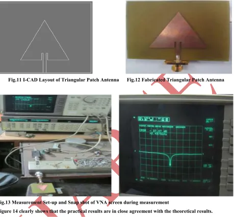
III FABRICATION
Fig.11 I-CAD Layout of Triangular Patch Antenna Fig.12 Fabricated Triangular Patch Antenna
Fig.13 Measurement Set-up and Snap shot of VNA screen during measurement
Figure 14 clearly shows that the practical results are in close agreement with the theoretical results.
IV RESULTS AND CONCLUSION
Following table 1 provides the comparison of result obtained through simulation and then fabrication.
TABLE 1
COMPARISON OF RESULTS OBTAINED
S.No Parameter Simulation Results V.N.A Results
1 Resonating Frequency 2.40 2.49
2 Return Loss -26 dB -37.4 dB
3 10 dB B.W. 67 MHz 65 MHz
The proposed design of triangular patch antenna has close agreement between simulated and measured results. The designed antenna can be used for Wi-Fi application. It can be used to form array also.
REFERENCES
1. C. Balanis, Yntenna Theory”, Jonh Wisley & Sons, Inc.1982
2. 1.J. Bahl and P. Bhartia, “Microstrip Antennas”, Artech House, Inc., 1980.
3. D. M. Pozar and D. H. Shaubert, “Microship antennas: the analysis and design of microstripantennas and arrays”, IEEE Press, Inc., 1995
4. Azhari Asrokin, Mohd Kamal Abd. Rahim, Mohd Haizal Jamaluddin and Mohd Riduan Ahmad “Triangular and Circular Dual Band Microstrip Antenna for WLAN Application” International RF And Microwave
Conference Proceedings, September 12 - 14, 2006, Putrajaya, Malaysia.
5. M. Ramesh, K. B. Yip, Design Inset Fed Microstrip Antenna, Microwaves & RF, Volume 42, Issue 12, Dec.